Embed Size (px)
Citation preview
MC542
Organização de ComputadoresTeoria e Prática
MC5422.1
2007 - 2011
Prof. Paulo Cesar Centoducatte
www.ic.unicamp.br/~ducatte
MC542
Circuitos Lógicos
Portas Lógicas, Tecnologia
MC5422.2
Portas Lógicas, Tecnologia
“DDCA” - (Capítulo 1)
“FDL” - (Capítulo 3)

Portas Lógicas, TecnologiaSumário
• Variáveis e Funções– Funções AND, Or e NOT
– Funções Complexas
– Tabela Verdade
• Portas Lógicas– Uma Entrada
– Duas Entradas
MC5422.3
– Duas Entradas
– Múltiplas Entradas
• Rede Lógica
• Níveis Lógicos– Margem de Ruído
• Característica de Transferência DC
• Família Lógicas

Portas Lógicas, TecnologiaSumário
• Transistor como Chave– NMOS
– PMOS
• Portas Lógicas com NMOS
• Portas Lógicas com CMOS
• Fan-In e Fan-Out
MC5422.4
• Fan-In e Fan-Out
• Tri-state
• Transmission Gates

Variáveis e Funções
Analogia com chaves controladas
MC5422.5
x 1 = x 0 =
S
x

S
Variáveis e Funções
MC5422.6
x L Battery Light
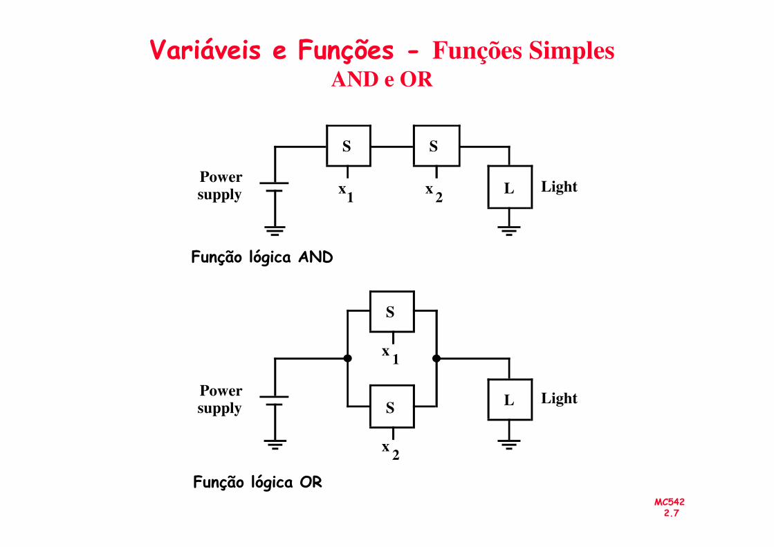
Função lógica AND
S
x1
LPowersupply
S
x2
Light
Variáveis e Funções - Funções SimplesAND e OR
MC5422.7
S
x1
LPowersupply S
x2
Função lógica OR
Light

S
x 1
L Power supply S Light
S
x 3
Variáveis e Funções - Funções Complexas
MC5422.8
Arranjo serie/paralelo
L supply S
x 2
Light x 3

S x L
Power
supply
R
Variáveis e FunçõesNOT
MC5422.9
S x L
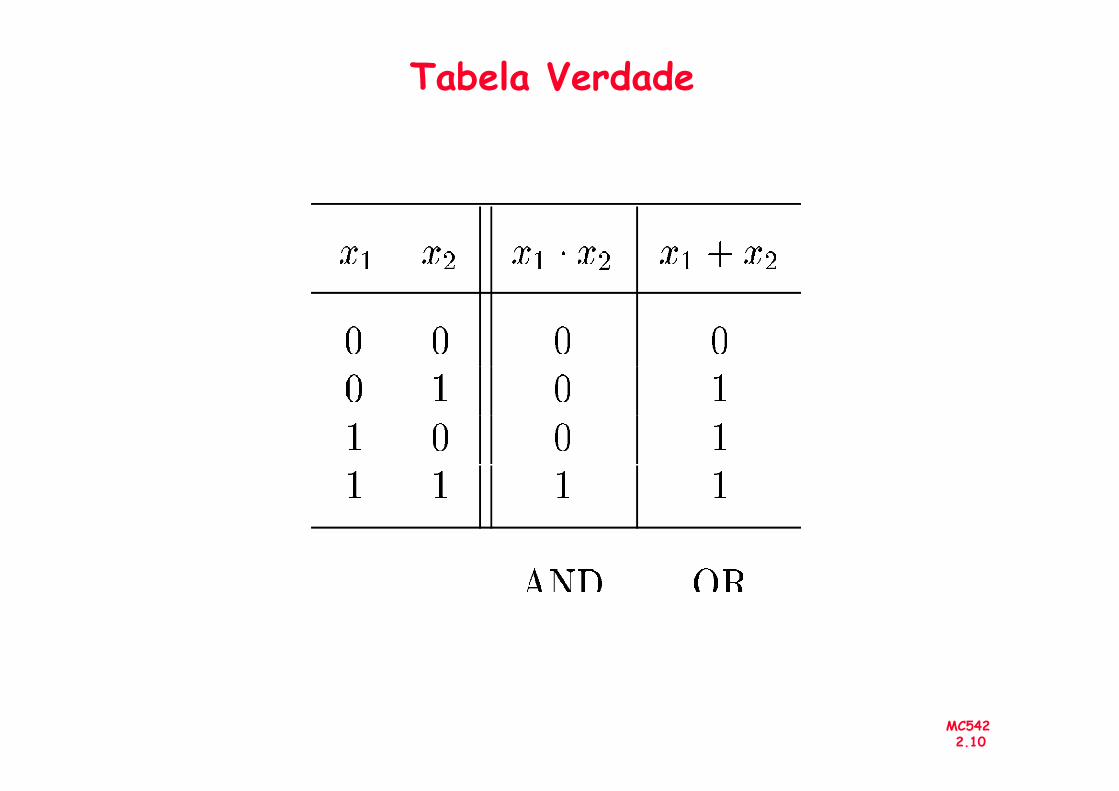
Tabela Verdade
MC5422.10

Tabela Verdade
MC5422.11
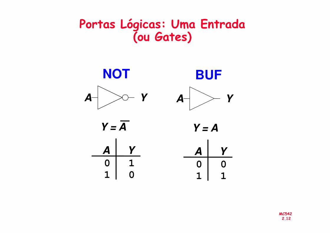
Portas Lógicas: Uma Entrada(ou Gates)
NOT
A Y
BUF
A Y
MC5422.12
Y = A
A Y0 1
1 0
Y = A
A Y0 0
1 1
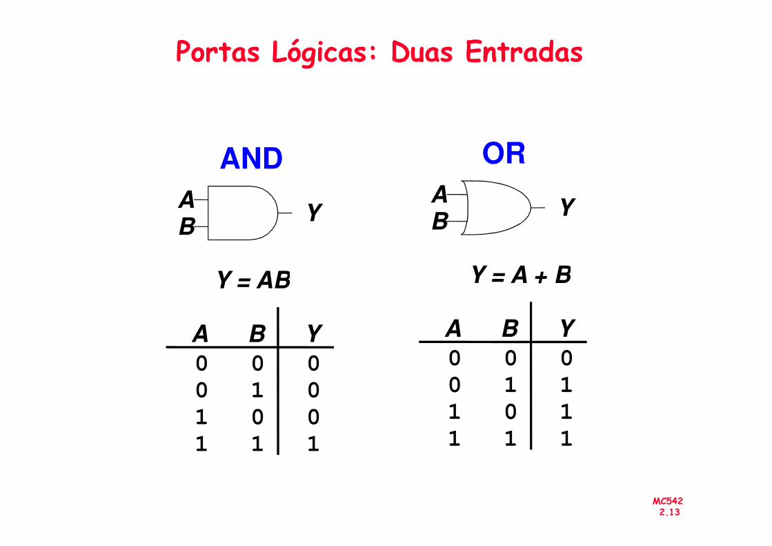
Portas Lógicas: Duas Entradas
AND
Y = AB
AB
Y
OR
Y = A + B
AB
Y
MC5422.13
Y = AB
A B Y0 0 0
0 1 0
1 0 0
1 1 1
Y = A + B
A B Y0 0 0
0 1 1
1 0 1
1 1 1

Portas Lógicas: Duas Entradas
XNOR
AB
Y
XOR NAND NOR
AB
YAB
YAB
Y
MC5422.14
Y = A + B
A B Y0 0
0 1
1 0
1 1
Y = A + B Y = AB Y = A + B
A B Y0 0 0
0 1 1
1 0 1
1 1 0
A B Y0 0 1
0 1 1
1 0 1
1 1 0
A B Y0 0 1
0 1 0
1 0 0
1 1 0
1
0
0
1
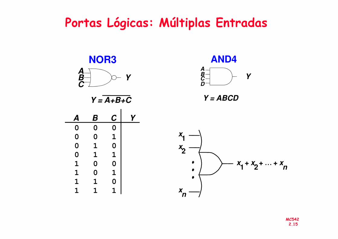
Portas Lógicas: Múltiplas Entradas
NOR3
Y = A+B+C
B C Y
AB YC
A
AND4
Y = ABCD
AB YCD
MC5422.15
x 1
x 2
x n
x 1
x 2
… … … … x n
+ + +
B C Y0 0
0 1
1 0
1 1
A0
0
0
0
0 0
0 1
1 0
1 1
1
1
1
1
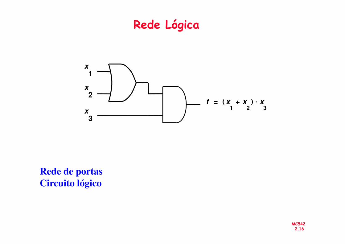
x 1
x 2
x 3
f x 1
x 2
+ ( ( ( ( ) ) ) ) x 3
⋅⋅⋅⋅=
Rede Lógica
MC5422.16
3
Rede de portas
Circuito lógico
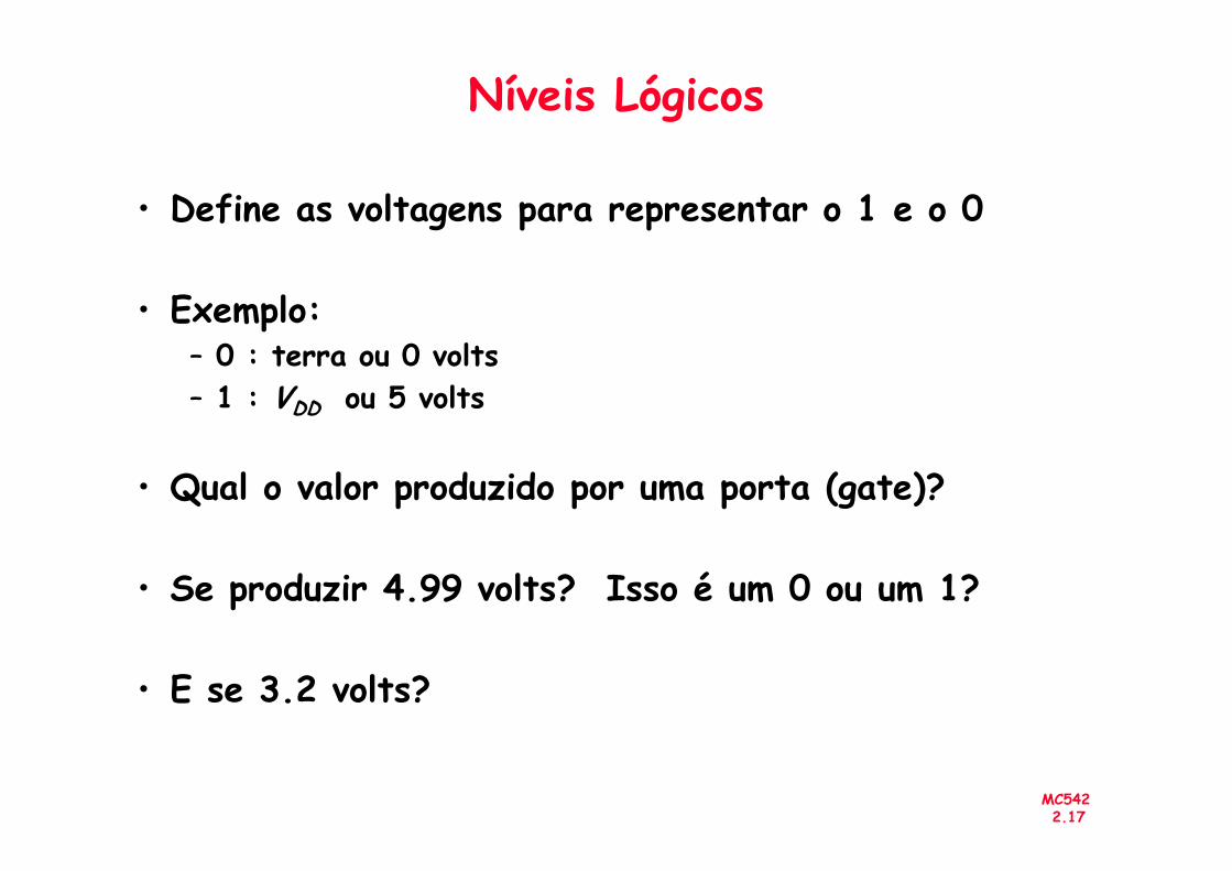
Níveis Lógicos
• Define as voltagens para representar o 1 e o 0
• Exemplo: – 0 : terra ou 0 volts
– 1 : VDD ou 5 volts
MC5422.17
• Qual o valor produzido por uma porta (gate)?
• Se produzir 4.99 volts? Isso é um 0 ou um 1?
• E se 3.2 volts?
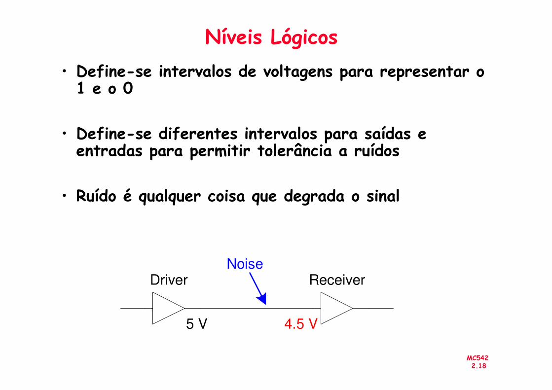
Níveis Lógicos
• Define-se intervalos de voltagens para representar o 1 e o 0
• Define-se diferentes intervalos para saídas e entradas para permitir tolerância a ruídos
• Ruído é qualquer coisa que degrada o sinal
MC5422.18
• Ruído é qualquer coisa que degrada o sinal
Driver ReceiverNoise
5 V 4.5 V

Níveis Lógicos
Logic value 1
Voltage
V DD
V 1,min
MC5422.19
Undefined
Logic value 0
V 1,min
V 0,max
V SS (Gnd)

Níveis Lógicos: Margem de Ruído
NMH
Input CharacteristicsOutput Characteristics
VO H
VDD
V
Logic High
Input Range
Logic High
Output Range
Driver Receiver
MC5422.20
Forbidden
Zone
NML
VO L
GND
VIH
VIL
Logic Low
Input RangeLogic Low
Output Range
NMH = VOH – VIH
NML = VIL – VOL
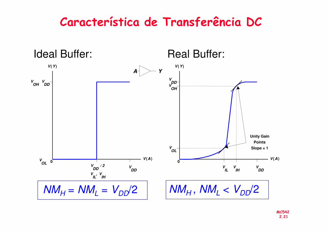
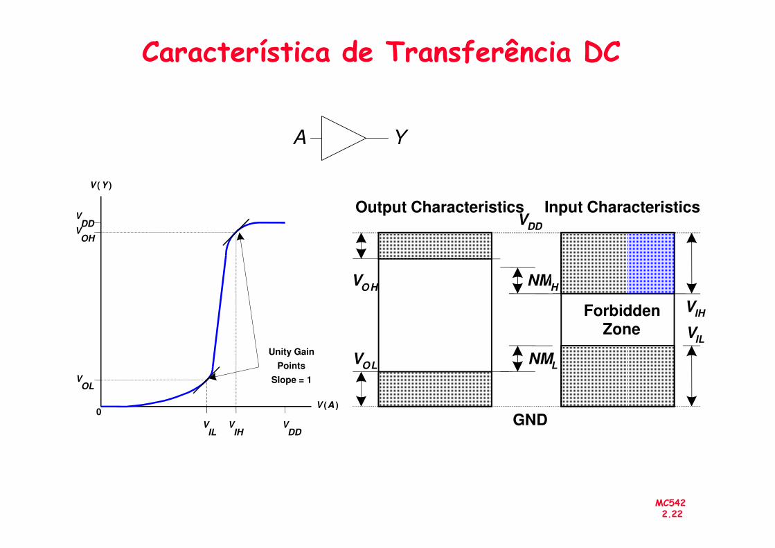
Característica de Transferência DC
Ideal Buffer: Real Buffer:V ( Y )
VOH
VDD
A YV ( Y )
VOH
VDD
MC5422.21
NMH = NML = VDD/2 NMH , NML < VDD/2
VDD
V (A )VOL
VIL
, VIH
0
VDD
V (A )
VOL
VIL
VIH
Unity Gain
Points
Slope = 1
0V
DD/ 2
Característica de Transferência DC
A Y
V (Y )
VOH
VDD
NM
Input CharacteristicsOutput CharacteristicsVDD
V
MC5422.22
VDD
V (A )
VOL
VIL
VIH
Unity Gain
Points
Slope = 1
0
ForbiddenZone
NML
NMH
VOL
GND
VIH
VIL
VOH

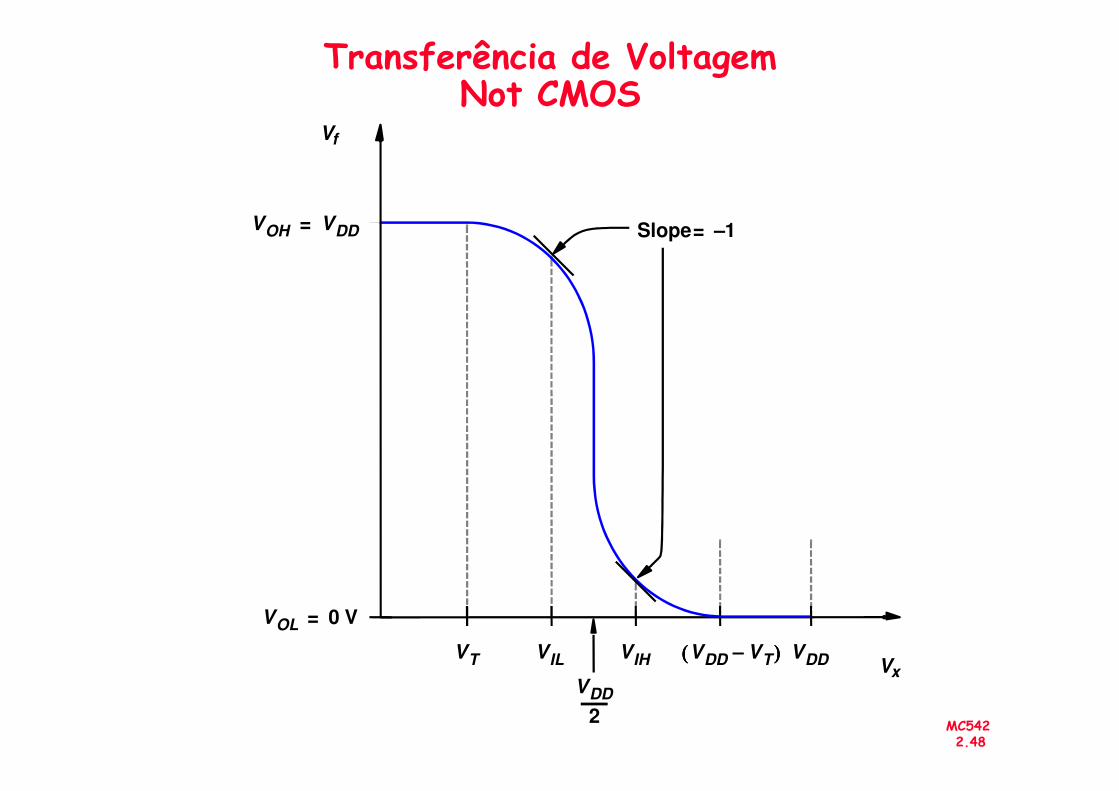
Característica de Transferência DC V f
V OH V DD= Slope 1 –=
MC5422.23
V x
V OL 0 V =
V T V IL V IH V DD V T –( ( ( ( ) ) ) ) V DD
V DD
2 —

Famílias Lógicas
Logic Family VDD VIL VIH VOL VOH
TTL 5 (4.75 - 5.25) 0.8 2.0 0.4 2.4
CMOS 5 (4.5 - 6) 1.35 3.15 0.33 3.84
LVTTL 3.3 (3 - 3.6) 0.8 2.0 0.4 2.4
MC5422.24
LVTTL 3.3 (3 - 3.6) 0.8 2.0 0.4 2.4
LVCMOS 3.3 (3 - 3.6) 0.9 1.8 0.36 2.7

Como Construir as Portas Lógicas
NOT
Y = A
A Y
A Y
BUF
Y = A
A Y
A Y
AND
Y = AB
A B Y
A
BY
OR
Y = A + B
A B Y
A
BY
MC5422.25
A Y
0 1
1 0
A Y
0 0
1 1
A B Y
0 0 0
0 1 0
1 0 0
1 1 1
A B Y
0 0 0
0 1 1
1 0 1
1 1 1
Transistores!
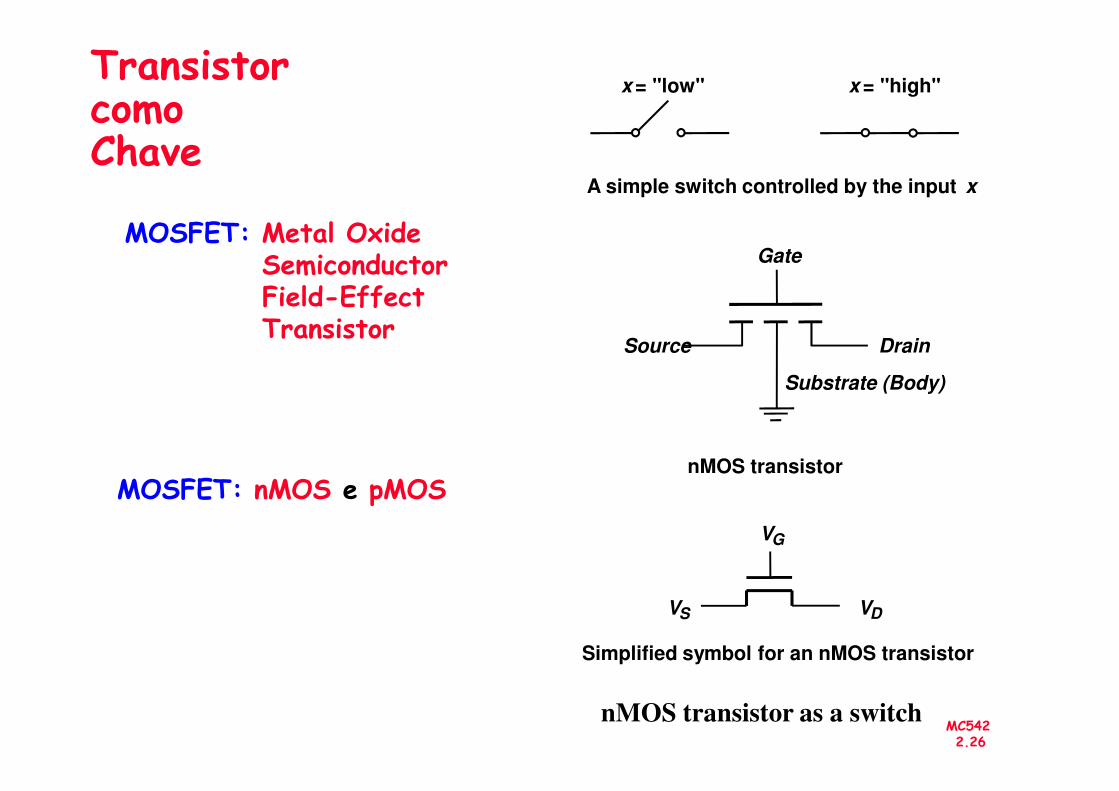
Transistor como Chave
Drain Source
x = "low" x = "high"
A simple switch controlled by the input x
Gate
Substrate (Body)
MOSFET: Metal Oxide SemiconductorField-Effect Transistor
MC5422.26
nMOS transistor as a switch
V D V S
nMOS transistor
Simplified symbol for an nMOS transistor
V G
MOSFET: nMOS e pMOS

Transistorcomo Chave
Gate
x = "high" x = "low"
A switch with the opposite behavior of Figure 3.2
V DD
Drain Source
Substrate (Body)
MC5422.27
pMOS transistor as a switch
V G
V D V S
pMOS transistor
Simplified symbol for an pMOS transistor
Substrate (Body)

Comportamento dos Transistores NMOS e PMOS em Circuitos
Transistor nMOS
V G
V D
V S = 0 V
Closed switch
when V G = V DD
V D = 0 V
Open switch
when V G = 0 V
V D
MC5422.28
V S = V DD
V D
V G
Open switch
when V G = V DD
V D
V DD
Closed switch
when V G = 0 V
V D = V DD
V DD
Transistor pMOS

• Transistores são construídos com silício, um semicondutor
• Silício não é condutor (não tem cargas livres)
• Quando dopado torna-se condutor (tem cargas livres)– n-type
– p-type
Transistores
MC5422.29
Silicon Lattice
Si SiSi
Si SiSi
Si SiSi
As SiSi
Si SiSi
Si SiSi
B SiSi
Si SiSi
Si SiSi
-
+
+
-
Free electron Free hole
n-Type p-Type

Transistor MOS
gatesource drain
SiO2
gatesource drainPolysilicon
MC5422.30
n
p substraten
nMOS
n p p
pMOS
gate
source drain
gate
source drain
substrate

CMOS: Fabricação e Comportamento
SiO 2
V S
0 V =
V G
0 V =
V
Transistor nMOS - off
MC5422.31
++++++ ++++ +++++++++ +++ ++++++
++++++ +++++++++ ++++++
+++++++++ +++++++++
+++++++++++ ++ +++++++++++
Drain (type n)Source (type n)
Substrate (type p)
When V GS
= 0 V, the transistor is off
S V
+++++++++
D

CMOS: Fabricação e Comportamento
Transistor nMOS - on
SiO 2
V DD
V 0 V =
V G
5 V =
V S
0 V =
MC5422.32
++++++ ++++ +++ ++++++++++++ ++++++
+++++++++++ +++++++++++++++++++++++ +++++++++++++++++
Channel (type n)
When V GS = 5 V, the transistor is on
++ ++++++++
V D
0 V = S
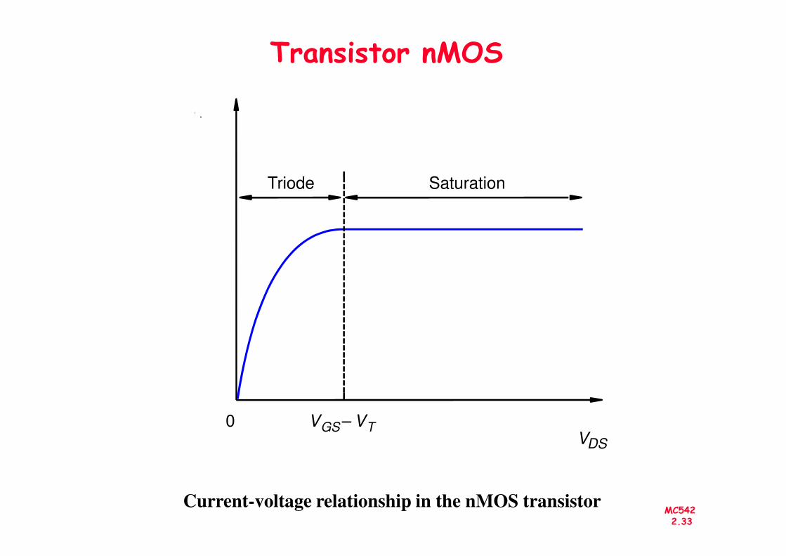
Transistor nMOS
I
D
Triode Saturation
MC5422.33
Current-voltage relationship in the nMOS transistor
0 V DS
V GS V T –

Portas Lógicas com nMOS
V x
V f
V DD
x f
R
V x
V f
R
+
-5 V
MC5422.34
Simplified circuit diagram Graphical symbols
x f
Circuit diagram
A NOT gate built using nMOS technology

Portas Lógicas com nMOS(NAND)
V f
V DD
f
0 0 1
0 1 0
1 1 1
x 1 x 2 f
V x 1
x 1 x 2
MC5422.35
Circuito Símbolo graficoTabela Verdade
f
1 1
0 1
1 0
V x 2 x 1 x 2

Portas Lógicas com nMOS(NOR)
V x 1 V x 2
V f
V DD
0
0
0
1
1
0
x 1
x 2 f
MC5422.36
1 2
(a) Circuit
(c) Graphical symbols
(b) Truth table
f
1
1
0
1
0
0
f
x 1
x 2
x 1
x 2
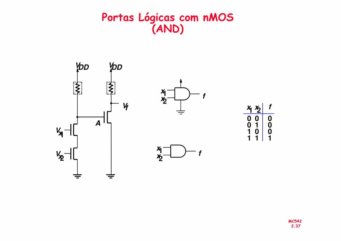
Portas Lógicas com nMOS(AND)
f
0 0 0
x 1 x 2 f V f
V DD
A
x 1 x 2
V DD
MC5422.37
f
0 0 1 1
0 1 0 1
0 0 0 1
A V x 1
V x 2
x 1 x 2

Portas Lógicas com nMOS(OR)
0
0
0
1
0
1
x 1
x 2 f
V f
V DD
V x 2 V x 1
V DD
MC5422.38
(a) Circuit (b) Truth table
f
0
1
1
1
0
1
1
1
1
f
V x 2 V x 1
x 1
x 2
x 1
x 2

Estrutura de um Circuito nMOSV DD
MC5422.39
V f
Pull-down network
V x 1
V x n
(PDN)

Estrutura de um Circuito CMOS(nMOS + pMOS)
A função é implementada por uma rede nMOS e uma pMOS simultaneamente
V DD
Pull-up network
(PUN)
MC5422.40
V f
Pull-down network
V x 1
V x n
(PDN)

NOT CMOS
V DD
T 1
f x T 1
T 2
MC5422.41
V f V x
T 2
on
off
off
on
1
0
0
1

NAND CMOS
V f
V DD
T 1 T 2
PUN
f = x11 + x2
MC5422.42
(a) Circuit (b) Truth table and transistor states
on
on
on
off
0
1
0
0
1
1
0
1
off
off
on
off
off
on
f
off
on
1
1
1
0
off
off
on
on
V x 1
V x 2
T 3
T 4
x 1 x 2 T 1 T 2 T 3 T 4
PDN
f = x1.x2
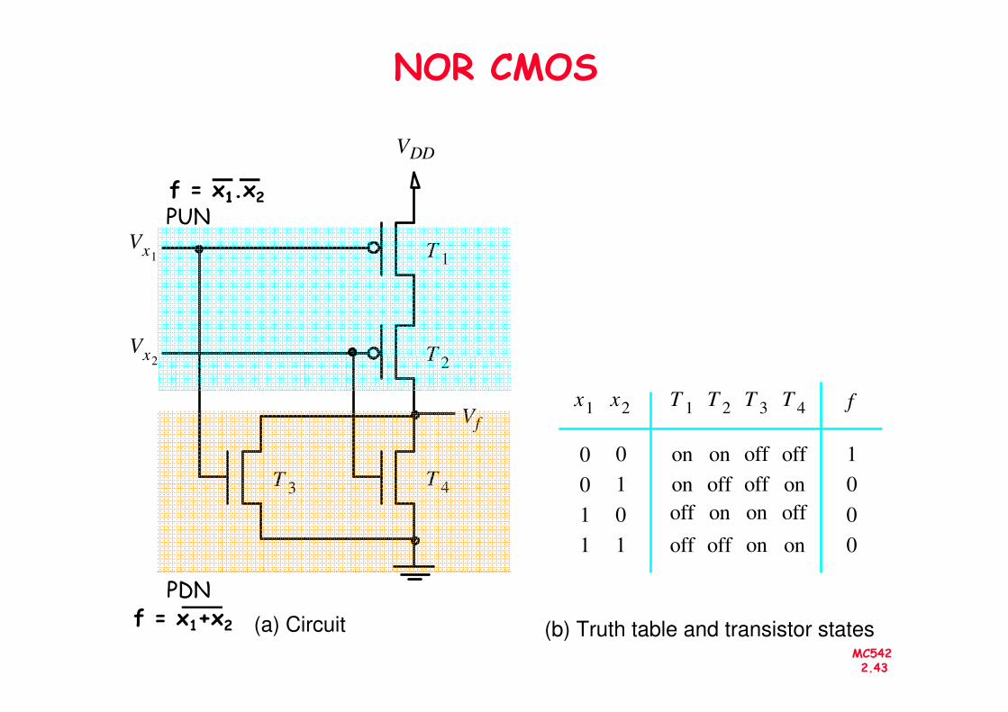
NOR CMOS
V DD
V x 1
V x 2
T 1
T 2
PUN
f = x11.x2
MC5422.43
(a) Circuit
V f
(b) Truth table and transistor states
on
on
on
off
0
1
0
0
1
1
0
1
off
off
on
off
off
on
f
off
on
1
0
0
0
off
off
on
on
V x 2 T 2
T 3 T 4
x 1 x 2 T 1 T 2 T 3 T 4
PDN
f = x1+x2
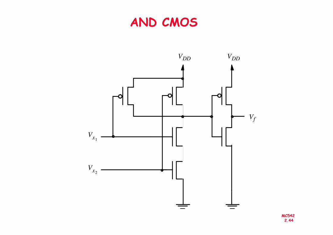
AND CMOS
V f
V DDV DD
MC5422.44
V f
V x 1
V x 2
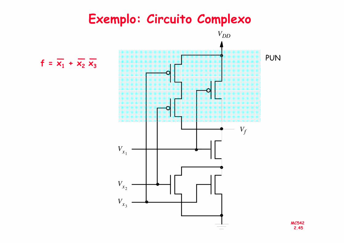
Exemplo: Circuito ComplexoV DD
f = x1 + x2 x3PUN
MC5422.45
V f
V x 1
V x 2
V x 3

Exercício
V f
V DD
Qual a função implementada por:
f = x (x x + x )
MC5422.46
V x 1
V x 2
V x 3
V x 4
f = x1 (x2x3 + x4)
PDN

Tensões em um Not nMOS
V DD
I stat
R
V f V OL= V f
V DD
MC5422.47
V x = 5 V
I stat
R DS
f OL
nMOS NOT gate
f
V x
Transferência de VoltagemNot CMOS
V f
V OH V DD= Slope 1 –=
MC5422.48
V x
V OL 0 V =
V T V IL V IH V DD V T –( ( ( ( ) ) ) ) V DD
V DD
2 —
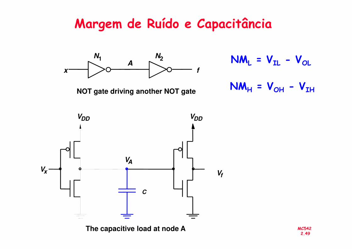
Margem de Ruído e Capacitância
NML = VIL - VOL
NMH = VOH - VIH
V DD V DD
x f A
NOT gate driving another NOT gate
N 1 N 2
MC5422.49
The capacitive load at node A
V f V x
C
V A

Margem de Ruído e Capacitância
V DD
Gnd
V x 50% 50%
MC5422.50
Propagation delay
V DD
Gnd
V A
90%
Propagation delay
10%
t r
50%
90%
50%
10%
t f

Transistor MOS
W 1
+ W 2
MC5422.51
Small transistor
L
W 1
L
Larger transistor
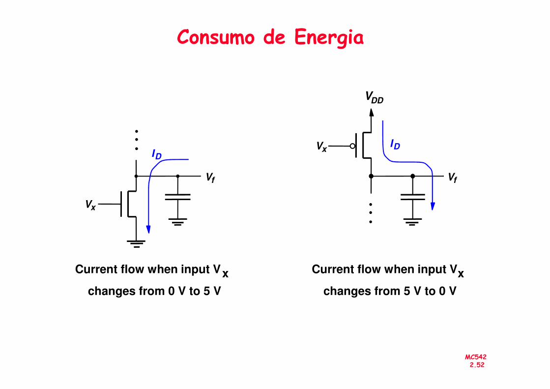
Consumo de Energia
VDD
Vf
IDVx
Vf
ID
MC5422.52
Vx
Current flow when input Vx
changes from 0 V to 5 V
Current flow when input Vx
changes from 5 V to 0 V
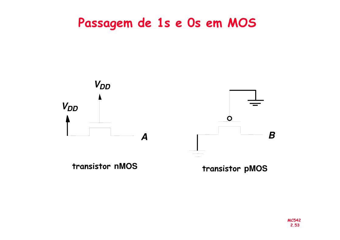
Passagem de 1s e 0s em MOS
V DD
V DD
MC5422.53
transistor nMOS transistor pMOS
A B

Implementação “pobre” de um AND CMOS
V f f x 1 x 2 V f
Voltage Logic
value Logic
value
MC5422.54
AND gate circuit
V DD
Truth table and voltage levels
V x 1
V x 2
1.5 V
1.5 V
0
1
0
0
1
1
0
1
1.5 V
3.5 V
f
0
0
0
1
x 1 x 2 V f
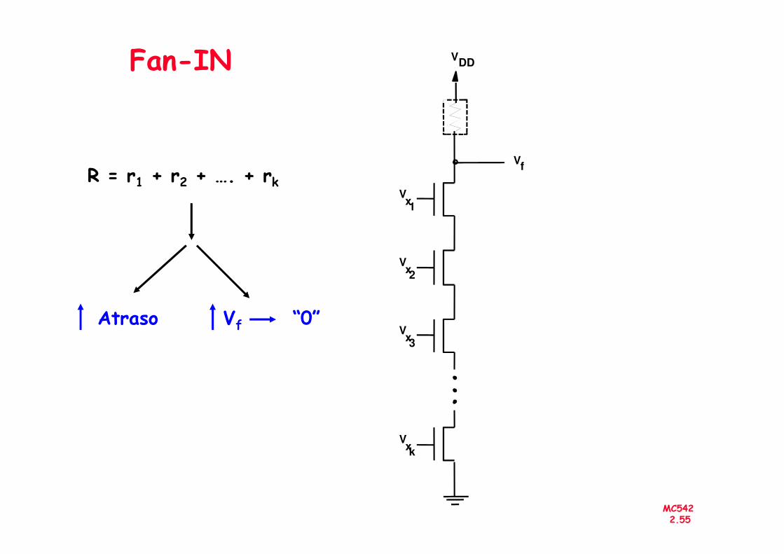
Fan-IN
V f
V DD
V x 2
V x 1
R = r1 + r2 + …. + rk
MC5422.55
2
V x 3
V x k
Atraso Vf “0”
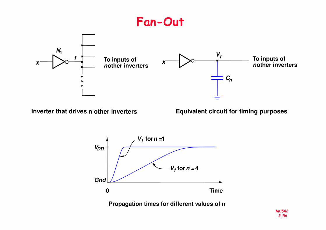
Fan-Out
Equivalent circuit for timing purposes
x f
inverter that drives n other inverters
To inputs ofn other inverters
To inputs ofn other inverters
C n
x
V f N 1
MC5422.56
forn = 1 V f
forn = 4 V f
V DD
Gnd
Time0
Propagation times for different values of n

Buffer
V f
V DD
V x
MC5422.57
Implementation of a buffer
x f
Graphical symbol
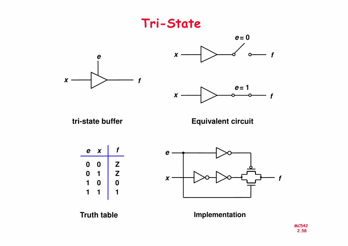
Tri-State
Equivalent circuit
x f
e
tri-state buffer
x f
e = 0
e = 1x f
MC5422.58
Equivalent circuit
Truth table
tri-state buffer
0
0
1
1
0
1
0
1
Z
Z
0
1
f e x
f x
e
Implementation
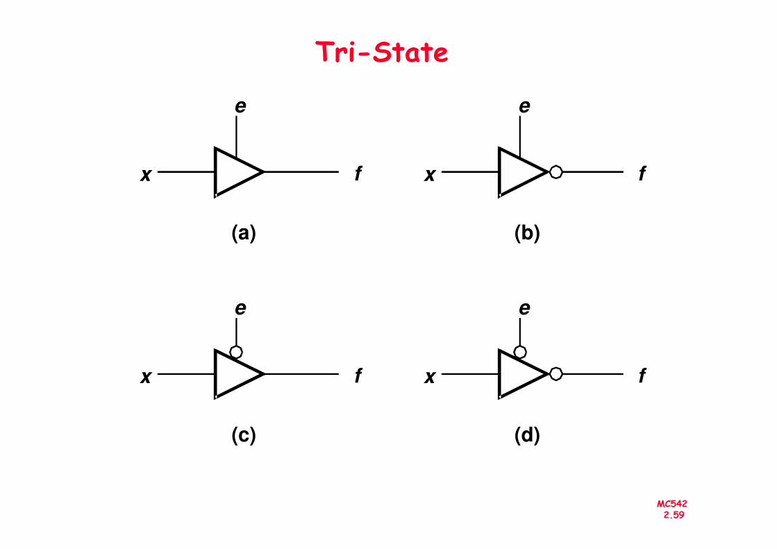
Tri-State
x f
e
(b)
x f
e
(a)
MC5422.59
x f
e
(c)
x f
e
(d)
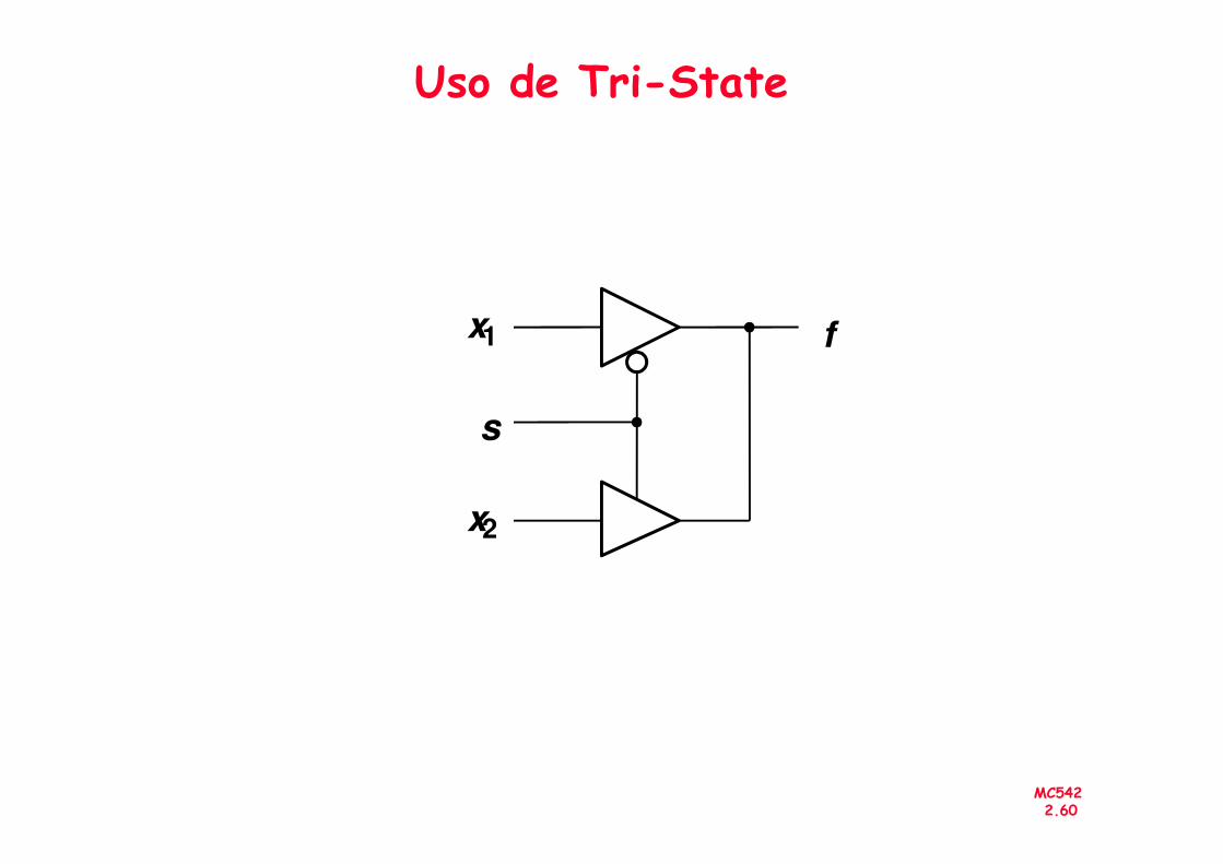
Uso de Tri-State
f x 1
s
MC5422.60
x 2
s
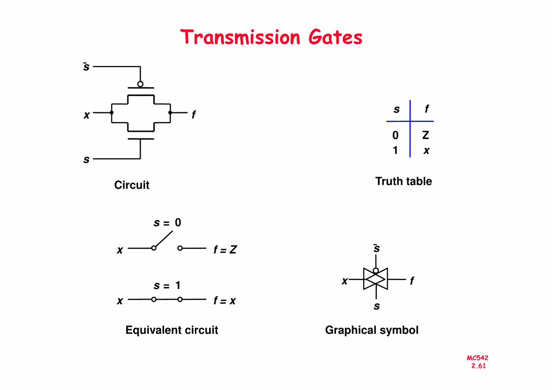
Transmission Gates
Circuit
f x
Truth table
Z
x
0
1
f s
s
s
MC5422.61
s 0 =
s 1 =
x
x
f = Z
f = x
Equivalent circuit Graphical symbol
f x
s
s
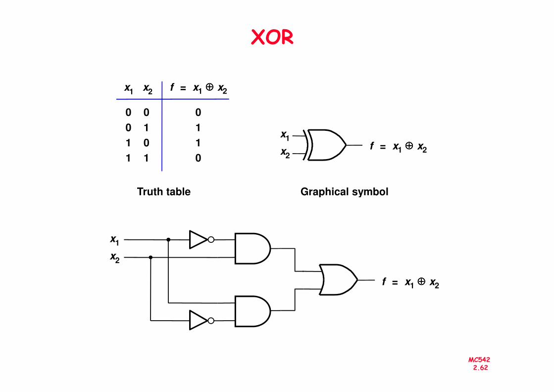
XOR
Graphical symbolTruth table
0
0
1
1
0
1
0
1
0
1
1
0
x 1 x 2
x 1
x 2
f x 1 x 2 ⊕ ⊕ ⊕ ⊕ =
f x 1 x 2 ⊕ ⊕ ⊕ ⊕ =
MC5422.62
Graphical symbolTruth table
f x 1 x 2 ⊕ ⊕ ⊕ ⊕ =
x 1
x 2
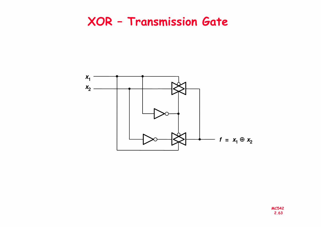
XOR – Transmission Gate
x 1
x 2
MC5422.63
f x 1 x 2 ⊕ ⊕ ⊕ ⊕ =
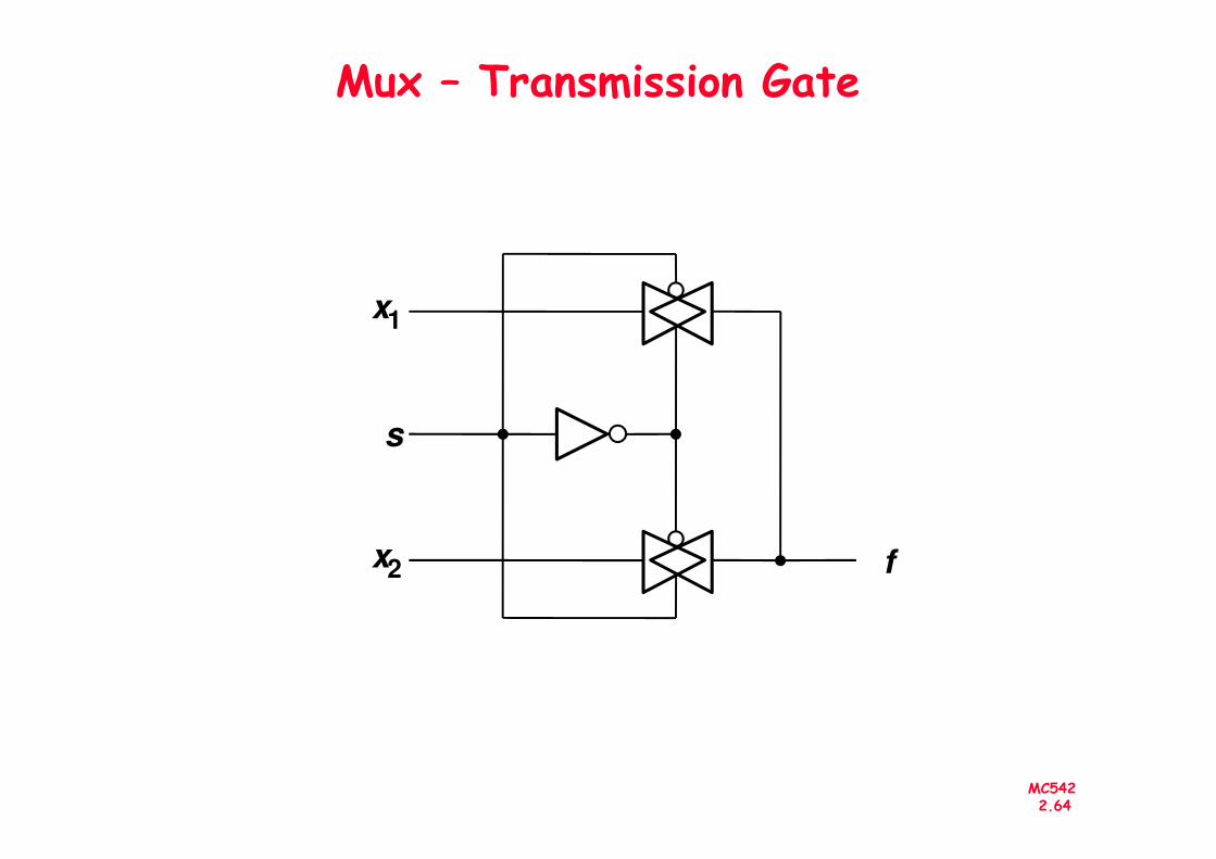
Mux – Transmission Gate
x 1
s
MC5422.64
x 2 f
s