Embed Size (px)
Citation preview
Fonte simétrica de 25mA com amplificador operacional, a partir de uma bateria
Descrição do circuitoAlgumas vezes precisamos utilizar uma fonte simétrica para alimentar um circuito analógico e a única fonte de alimentação é uma
bateria ou conjunto de pilhas. Neste caso, é possível criar a fonte simétrica utilizando um amplificador operacional. Para isso basta gerar a tensão média com resistores e aplicar esta tensão ao amplificador, que manterá este valor constante na saída.
Para isso é utilizada uma configuração especial, conhecida geralmente como buffer, onde a tensão aplicada na estrada é a mesma na saída. O ganho é unitário, a diferença está na impedância da entrada, que é altíssima e a da saída muito baixa.
Este modelo é muito utilizado em instrumentação industrial devido exatamente a impedância alta que não carrega os elementos primários, como por exemplo uma sonda de pH.
A impedância de entrada do 741 é de aproximadamente 2MΩ. Amplificadores modernos, com tecnologia FET têm impedâncias de até 500MΩ.
Os resistores R1 e R2 podem ter valores bastante altos, para evitar consumo desnecessário da fonte, porém cuidado com a impedância interna do operacional. A saída é limitada à corrente máxima do componente, que no caso do 741 fica em torno de 25mA. Para correntes maiores é necessário acrescentar um amplificador de corrente com transistores em push-pull na saída.
Os capacitores devem ter tensão pelo menos 50% superior ao valor que serão submetidos. Sugestão: 63V.
FuncionamentoEste circuito opera com tensões a partir de aproximadamente 5V de uma bateria, conjunto de pilhas ou fonte. A saída será a metade da alimentação.
Por exemplo, se for alimentado com uma bateria de 9V, terá as tensões de +4,5V e -4,5V.
Não ultrapasse os 30V, típico limite deste amplificador.
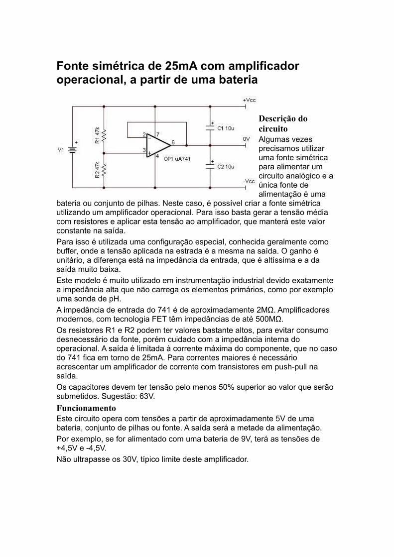
_______________General DescriptionThe MAX1044 and ICL7660 are monolithic, CMOSswitched-capacitor voltage converters that invert, dou-ble, divide, or multiply a positive input voltage. They arepin compatible with the industry-standard ICL7660 andLTC1044. Operation is guaranteed from 1.5V to 10V withno external diode over the full temperature range. Theydeliver 10mA with a 0.5V output drop. The MAX1044has a BOOST pin that raises the oscillator frequencyabove the audio band and reduces external capacitorsize requirements.
The MAX1044/ICL7660 combine low quiescent currentand high efficiency. Oscillator control circuitry and fourpower MOSFET switches are included on-chip.Applications include generating a -5V supply from a+5V logic supply to power analog circuitry. For applica-tions requiring more power, the MAX660 delivers up to100mA with a voltage drop of less than 0.65V.
________________________Applications-5V Supply from +5V Logic Supply
Personal Communications Equipment
Portable Telephones
Op-Amp Power Supplies
EIA/TIA-232E and EIA/TIA-562 Power Supplies
Data-Acquisition Systems
Hand-Held Instruments
Panel Meters
____________________________Features♦ Miniature µMAX Package
♦ 1.5V to 10.0V Operating Supply Voltage Range
♦ 98% Typical Power-Conversion Efficiency
♦ Invert, Double, Divide, or Multiply Input Voltages
♦ BOOST Pin Increases Switching Frequencies(MAX1044)
♦ No-Load Supply Current: 200µA Max at 5V
♦ No External Diode Required for Higher-VoltageOperation
______________Ordering Information
Ordering Information continued at end of data sheet.* Contact factory for dice specifications.
MA
X1
04
4/IC
L7
66
0
Switched-Capacitor Voltage Converters
________________________________________________________________ Maxim Integrated Products 1
Call toll free 1-800-998-8800 for free samples or literature.
19-4667; Rev 1; 7/94
MAX1044 ICL7660
4
3
2
1
CAP-
GND
CAP+
(N.C.) BOOST
5
6
7
8
VOUT
LV
OSC
V+
TOP VIEW
( ) ARE FOR ICL7660
DIP/SO/µMAX
TO-99
ICL7660
N.C.
CAP+
GND
CAP-
VOUT
LV
OSC
V+ AND CASE
1
2
3
4
5
6
7
8
_________________Pin Configurations
NEGATIVE VOLTAGE CONVERTER
CAP+
CAP-
V+
VOUT
GND
INPUT SUPPLY VOLTAGE
NEGATIVE OUTPUT VOLTAGE
MAX1044 ICL7660
__________Typical Operating Circuit
Dice*
8 SO
8 Plastic DIP
PIN-PACKAGETEMP. RANGE
0°C to +70°C
0°C to +70°C
0°C to +70°CMAX1044C/D
MAX1044CSA
MAX1044CPA
PART
8 Plastic DIP-40°C to +85°CMAX1044EPA
MA
X1
04
4/I
CL
76
60
Switched-Capacitor Voltage Converters
2 _______________________________________________________________________________________
ABSOLUTE MAXIMUM RATINGS
ELECTRICAL CHARACTERISTICS(Circuit of Figure 1, V+ = 5.0V, LV pin = 0V, BOOST pin = open, ILOAD = 0mA, TA = TMIN to TMAX, unless otherwise noted.)
Stresses beyond those listed under “Absolute Maximum Ratings” may cause permanent damage to the device. These are stress ratings only, and functionaloperation of the device at these or any other conditions beyond those indicated in the operational sections of the specifications is not implied. Exposure toabsolute maximum rating conditions for extended periods may affect device reliability.
Note 1: The Maxim ICL7660 and MAX1044 can operate without an external output diode over the full temperature and voltageranges. The Maxim ICL7660 can also be used with an external output diode in series with pin 5 (cathode at VOUT) whenreplacing the Intersil ICL7660. Tests are performed without diode in circuit.
Note 2: fOSC is tested with COSC = 100pF to minimize the effects of test fixture capacitance loading. The 1pF frequency is correlat-ed to this 100pF test point, and is intended to simulate pin 7’s capacitance when the device is plugged into a test socketwith no external capacitor. For this test, the LV pin is connected to GND for comparison to the original manufacturer’sdevice, which automatically connects this pin to GND for (V+ > 3V).
Supply Voltage (V+ to GND, or GND to VOUT)....................10.5VInput Voltage on Pins 1, 6, and 7 .........-0.3V ≤ VIN ≤ (V+ + 0.3V)LV Input Current ..................................................................20µAOutput Short-Circuit Duration (V+ ≤ 5.5V)..................ContinuousContinuous Power Dissipation (TA = +70°C)
Plastic DIP (derate 9.09mW/°C above +70°C) ............727mWSO (derate 5.88mW/°C above +70°C).........................471mWµMAX (derate 4.1mW/°C above +70°C) ......................330mW
CERDIP (derate 8.00mW/°C above +70°C).................640mWTO-99 (derate 6.67mW/°C above +70°C)....................533mW
Operating Temperature RangesMAX1044C_ _ /ICL7660C_ _ ..............................0°C to +70°CMAX1044E_ _ /ICL7660E_ _ ............................-40°C to +85°CMAX1044M_ _ /ICL7660M_ _ ........................-55°C to +125°C
Storage Temperature Range ............................-65°C to + 150°CLead Temperature (soldering, 10sec) .............................+300°C
kHz
TA = 0°C to +70°C
TA = +25°C
TA = -55°C to +125°C
VOSC = 0V or V+, LV open
RL = 5kΩ, TA = +25°C, fOSC 5kHz, LV open
TA = -40°C to +85°C
RL = 10kΩ, LV open
RL = 10kΩ, LV to GND
fOSC = 2.7kHz (ICL7660),fOSC = 1kHz (MAX1044),V+ = 2V, IL = 3mA,LV to GND
30 200RL = ∞,pins 1 and 7 no connection,LV open
µA
10
Supply Current
20
Pin 1 = 0V
Pin 1 = V+
3Oscillator Sink orSource Current
%95 98Power Efficiency
COSC = 1pF,LV to GND (Note 2)
400
1
Ω
325
Output Resistance
IL = 20mA, fOSC = 5kHz,LV open
200
TA = 0°C to +70°C
TA = -40°C to +85°C
200
UNITSMAX1044
MIN TYP MAXPARAMETER
325
TA = +25°C
130
325
130
150
200
V1.5 10
Supply VoltageRange (Note 1)
65 100
5Oscillator Frequency
100V+ = 2VV+ = 5V
MΩ1.0Oscillator Impedance
80 175
95 98
400
300
250
225
ICL7660MIN TYP MAX
300
140
250
120
150
250
3.0 10.0
1.5 3.5
55 100
10
1001.0
TA = -55°C to +125°C
RL = ∞, pins 1 and 7 = V+ = 3V
TA = +25°C
TA = +25°C
TA = 0°C to +70°C
TA = -40°C to +85°C
TA = -55°C to +125°C
V+ = 5V
V+ = 2V
RL = ∞, TA = +25°C, LV open 99.0 99.9 %97.0 99.9Voltage Conversion Efficiency
µA
kΩ
CONDITIONS
80
90
100
30101
EFFICIENCY vs. OSCILLATOR FREQUENCY
70
MAX
1044
-Fig
7
OSCILLATOR FREQUENCY (Hz)
EFFI
CIEN
CY (%
)
104
50
40
102 103 6x10⁵
60
105
C1, C
2 =
100µ
F
C1, C
2 =
10µF
C1, C
2 =
1µF
EXTERNAL HCMOS OSCILLATOR
10,000
100,000
0.11
OSCILLATOR FREQUENCY vs. EXTERNAL CAPACITANCE
1000
MAX
1044
-Fig
8
COSC (pF)
OSCI
LLAT
OR F
REQU
ENCY
(Hz)
1000
10
1
10 100 100,000
100
10,000
ICL7660 and MAX1044 with BOOST = OPEN
MAX1044 with BOOST -V+
1001
OSCILLATOR FREQUENCY vs. SUPPLY VOLTAGE
MAX
1044
-Fig
9
SUPPLY VOLTAGE (V)
OSCI
LLAT
OR F
REQU
ENCY
(Hz)
4
10,000
1000
2 3 6 7 8 9 10
100,000
5
FROM TOP TO BOTTOM AT 5V MAX1044, BOOST = V+, LV = GND MAX1044, BOOST = V+, LV = OPEN ICL7660, LV = GND ICL7660, LV = OPEN MAX1044, BOOST = OPEN, LV = GND MAX1044, BOOST = OPEN, LV = OPEN
00 1 2 3 4 5 6 7 8 9 10
OUTPUT VOLTAGE and OUTPUT RIPPLE vs. LOAD CURRENT
-0.5
-2.0
MAX
1044
-Fig
1
LOAD CURRENT (mA)
OUTP
UT V
OLTA
GE (V
)
OUTP
UT R
IPPL
E (m
Vp-p
)
-1.5
-1.0
0
250
200
150
100
50
400
350
300
OUTPUT VOLTAGE
V+ = 2V LV = GND
OUTPUT RIPPLE
A: MAX1044 with BOOST = V+ B: ICL7660 C: MAX1044 with BOOST = OPEN
A
B
C
00 5 10 15 20 25 30 35 40
OUTPUT VOLTAGE and OUTPUT RIPPLE vs. LOAD CURRENT
-0.5
-2.0
-2.5
-3.0
-3.5
-4.0
-4.5
-5.0
MAX
1044
-Fig
2
LOAD CURRENT (mA)
OUTP
UT V
OLTA
GE (V
)
OUTP
UT R
IPPL
E (m
Vp-p
)
-1.5
-1.0
0
720
640
560
480
400
320
240
160
80
800OUTPUT VOLTAGE
OUTPUT RIPPLE
V+ = 5V LV = OPEN
A
A
B
C
B
C
A: MAX1044 with BOOST = V+ B: ICL7660 C: MAX1044 with BOOST = OPEN
00 5 10 15 20 25 30 35 40
OUTPUT VOLTAGE and OUTPUT RIPPLE vs. LOAD CURRENT
-1
-4
-5
-6
-7
-8
-9
-10
MAX
1044
-Fig
3
LOAD CURRENT (mA)
OUTP
UT V
OLTA
GE (V
)
OUTP
UT R
IPPL
E (m
Vp-p
)
-3
-2
0
700
630
560
490
420
350
280
210
140
70
V+ = 10V LV = OPEN
OUTPUT RIPPLE
A
B
A: MAX1044 with BOOST = V+ B: ICL7660 C: MAX1044 with BOOST = OPEN
C
BC
AOUTPUT VOLTAGE
00 1 2 3 4 5 6 7 8 9 10
EFFICIENCY and SUPPLY CURRENT vs. LOAD CURRENT
10
40
50
60
70
80
90
100
MAX
1044
-Fig
4
LOAD CURRENT (mA)
EFFI
CIEN
CY (%
)
SUPP
LY C
URRE
NT (m
A)
30
20
0
7
8
9
10
6
5
4
3
2
1
SUPPLY CURRENT
EFFICIENCY
V+ = 2V LV = GND
00 5 10 15 20 25 30 35 40
EFFICIENCY and SUPPLY CURRENT vs. LOAD CURRENT
10
40
50
60
70
80
90
100
MAX
1044
-Fig
5
LOAD CURRENT (mA)
EFFI
CIEN
CY (%
)
SUPP
LY C
URRE
NT (m
A)
30
20
0
35
40
45
50
30
25
20
15
10
5
V+ = 5V LV = OPEN
EFFICIENCY
A: MAX1044 with BOOST = V+ B: ICL7660 C: MAX1044 with BOOST = OPEN SUPPLY CURRENT
B
C
A
00 5 10 15 20 25 30 35 40
EFFICIENCY and SUPPLY CURRENT vs. LOAD CURRENT
10
40
50
60
70
80
90
100
MAX
1044
-Fig
6
LOAD CURRENT (mA)
EFFI
CIEN
CY (%
)
SUPP
LY C
URRE
NT (m
A)
30
20
0
35
40
45
50
30
25
20
15
10
5V+ = 10V LV = OPEN
A: MAX1044 with BOOST = V+ B: ICL7660 C: MAX1044 with BOOST = OPEN SUPPLY CURRENT
B, C
EFFICIENCY
A
MA
X1
04
4/IC
L7
66
0
Switched-Capacitor Voltage Converters
_______________________________________________________________________________________ 3
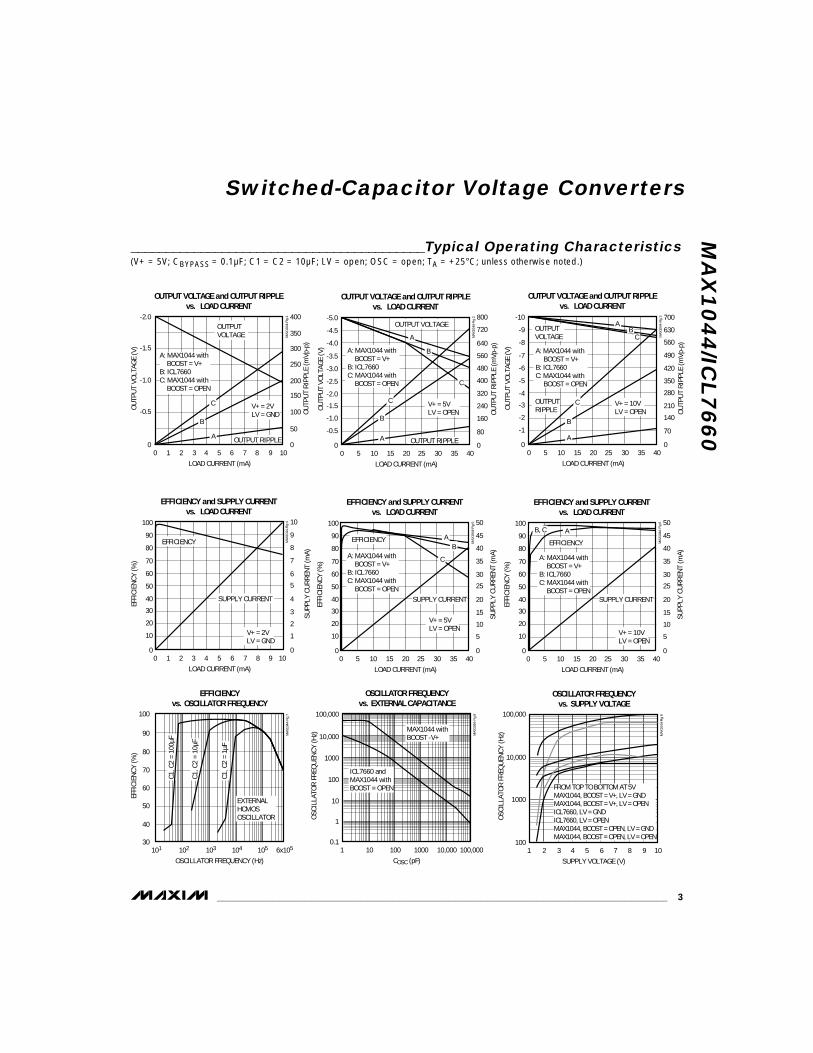
__________________________________________Typical Operating Characteristics(V+ = 5V; CBYPASS = 0.1µF; C1 = C2 = 10µF; LV = open; OSC = open; TA = +25°C; unless otherwise noted.)
0.11 2 3 4 5 6 7 8 9 10
QUIESCENT CURRENT vs. SUPPLY VOLTAGE
MAX
1044
-Fig
12
SUPPLY VOLTAGE (V)
QUIE
SCEN
T CU
RREN
T (µ
A)
10
1
100
10002000
AB
DC
A: MAX1044, BOOST = V+, LV = GND B: MAX1044, BOOST = V+, LV = OPEN C: ICL7660 and MAX1044 with BOOST = OPEN, LV = GND; ABOVE 5V, MAX1044 ONLY D: ICL7660 and MAX1044 with BOOST = OPEN, LV = OPEN
0101 102 103 104 105
OUTPUT RESISTANCE vs. OSCILLATOR FREQUENCY
MAX
1044
-Fig
14
FREQUENCY (Hz)
RESI
STAN
CE (Ω
)
200
100
300
400
500
600
700
800
900
1000
C1, C
2 =
100µ
F
C1, C
2 =
1µF
C1, C
2 =
10µF
EXTERNAL HCMOS OSCILLATOR
0-50 -25 0 25 50 75 100 125
QUIESCENT CURRENT vs. TEMPERATURE
MAX
1044
-Fig
13
TEMPERATURE (°C)
QUIE
SCEN
T CU
RREN
T (µ
A)
200
100
300
400500
ICL7660, MAX1044 with BOOST = OPEN
MAX1044 with BOOST = V+
01 2 3 4 5 6 7 8 9 10
OUTPUT RESISTANCE vs. SUPPLY VOLTAGE
MAX
1044
-Fig
15
SUPPLY VOLTAGE (V)
OUTP
UT R
ESIS
TANC
E (Ω
)
40
20
60
80
100
120
140
160
180
200
20-60 -40 -20 0 20 40 60 80 100 120 140
OUTPUT RESISTANCE vs. TEMPERATURE
MAX
1044
-Fig
16
TEMPERATURE (°C)
OUTP
UT R
ESIS
TANC
E (Ω
)
40
30
50
60
70
80
ICL7660, MAX1044 with BOOST = OPEN
MAX1044 with BOOST = V+
MA
X1
04
4/I
CL
76
60
Switched-Capacitor Voltage Converters
4 _______________________________________________________________________________________
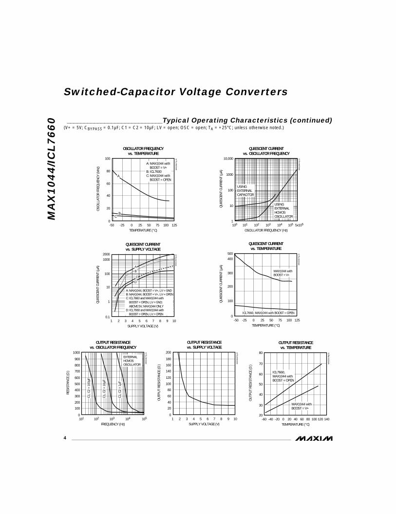
____________________________Typical Operating Characteristics (continued)(V+ = 5V; CBYPASS = 0.1µF; C1 = C2 = 10µF; LV = open; OSC = open; TA = +25°C; unless otherwise noted.)
0-50
OSCILLATOR FREQUENCY vs. TEMPERATURE
MAX
1044
-Fig
10
TEMPERATURE (°C)
OSCI
LLAT
OR F
REQU
ENCY
(kHz
)
25
40
20
-25 0 75 100 125
60
80
100
50
A: MAX1044 with BOOST = V+ B: ICL7600 C: MAX1044 with BOOST = OPEN
B
A
C1100 101 102 103 104 105 5x10⁵
QUIESCENT CURRENT vs. OSCILLATOR FREQUENCY
MAX
1044
-Fig
11
OSCILLATOR FREQUENCY (Hz)
QUIE
SCEN
T CU
RREN
T (µ
A)
100
10
1000
10,000
USING EXTERNAL HCMOS OSCILLATOR
USING EXTERNAL CAPACITOR
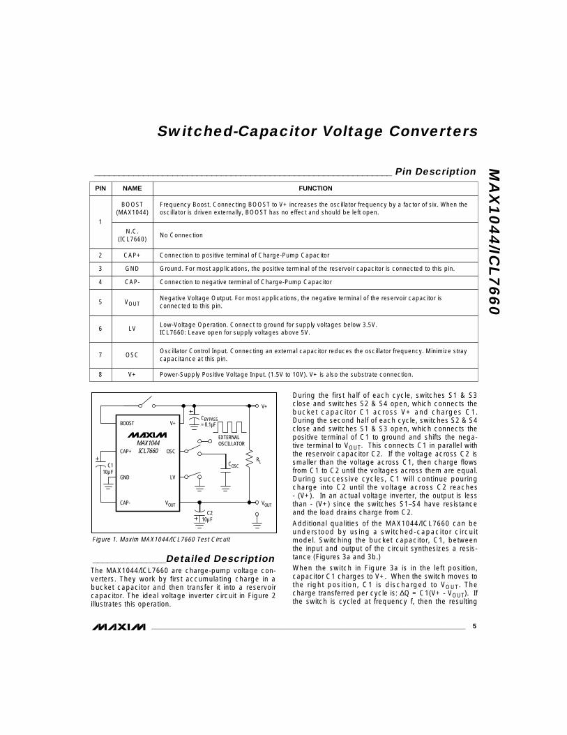
_______________Detailed DescriptionThe MAX1044/ICL7660 are charge-pump voltage con-verters. They work by first accumulating charge in abucket capacitor and then transfer it into a reservoircapacitor. The ideal voltage inverter circuit in Figure 2illustrates this operation.
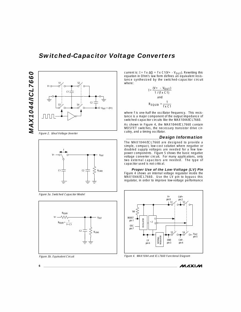
During the first half of each cycle, switches S1 & S3close and switches S2 & S4 open, which connects thebucket capacitor C1 across V+ and charges C1.During the second half of each cycle, switches S2 & S4close and switches S1 & S3 open, which connects thepositive terminal of C1 to ground and shifts the nega-tive terminal to VOUT. This connects C1 in parallel withthe reservoir capacitor C2. If the voltage across C2 issmaller than the voltage across C1, then charge flowsfrom C1 to C2 until the voltages across them are equal.During successive cycles, C1 will continue pouringcharge into C2 until the voltage across C2 reaches - (V+). In an actual voltage inverter, the output is lessthan - (V+) since the switches S1–S4 have resistanceand the load drains charge from C2.
Additional qualities of the MAX1044/ICL7660 can beunderstood by using a switched-capacitor circuitmodel. Switching the bucket capacitor, C1, betweenthe input and output of the circuit synthesizes a resis-tance (Figures 3a and 3b.)
When the switch in Figure 3a is in the left position,capacitor C1 charges to V+. When the switch moves tothe right position, C1 is discharged to VOUT. Thecharge transferred per cycle is: ∆Q = C1(V+ - VOUT). Ifthe switch is cycled at frequency f, then the resulting
MA
X1
04
4/IC
L7
66
0
Switched-Capacitor Voltage Converters
_______________________________________________________________________________________ 5
MAX1044 ICL7660
BOOST
CAP+
GND
CBYPASS = 0.1µF
V+
RL
CAP-
V+
OSC
C1 10µ F
LV
VOUT
C2 10µ F
COSC
EXTERNAL OSCILLATOR
VOUT
_____________________________________________________________ Pin Description
NAME FUNCTION
BOOST(MAX1044)
Frequency Boost. Connecting BOOST to V+ increases the oscillator frequency by a factor of six. When theoscillator is driven externally, BOOST has no effect and should be left open.
PIN
1N.C.
(ICL7660)No Connection
3 GND Ground. For most applications, the positive terminal of the reservoir capacitor is connected to this pin.
2 CAP+ Connection to positive terminal of Charge-Pump Capacitor
6 LVLow-Voltage Operation. Connect to ground for supply voltages below 3.5V.ICL7660: Leave open for supply voltages above 5V.
5 VOUTNegative Voltage Output. For most applications, the negative terminal of the reservoir capacitor isconnected to this pin.
4 CAP- Connection to negative terminal of Charge-Pump Capacitor
7 OSCOscillator Control Input. Connecting an external capacitor reduces the oscillator frequency. Minimize straycapacitance at this pin.
8 V+ Power-Supply Positive Voltage Input. (1.5V to 10V). V+ is also the substrate connection.
Figure 1. Maxim MAX1044/ICL7660 Test Circuit
MA
X1
04
4/I
CL
76
60 current is: I = f x ∆Q = f x C1(V+ - VOUT). Rewriting this
equation in Ohm’s law form defines an equivalent resis-tance synthesized by the switched-capacitor circuitwhere:
where f is one-half the oscillator frequency. This resis-tance is a major component of the output impedance ofswitched-capacitor circuits like the MAX1044/ICL7660.
As shown in Figure 4, the MAX1044/ICL7660 containMOSFET switches, the necessary transistor drive cir-cuitry, and a timing oscillator.
________________Design InformationThe MAX1044/ICL7660 are designed to provide a simple, compact, low-cost solution where negative ordoubled supply voltages are needed for a few low-power components. Figure 5 shows the basic negativevoltage converter circuit. For many applications, onlytwo external capacitors are needed. The type ofcapacitor used is not critical.
Proper Use of the Low-Voltage (LV) PinFigure 4 shows an internal voltage regulator inside theMAX1044/ICL7660. Use the LV pin to bypass this regulator, in order to improve low-voltage performance
I(V+ - V )
1 / (f x C1)
R1
f x C1
OUT
EQUIV
=
=
and
Switched-Capacitor Voltage Converters
6 _______________________________________________________________________________________
S1V+
S2
S3 S4
C1
C2
VOUT = -(V+)
Figure 2. Ideal Voltage Inverter
V+
C1
f
C2 RLOAD
VOUT
Figure 3a. Switched Capacitor Model
REQUIV =
REQUIV
VOUT
RLOAD
1
V+
f × C1
C2
Figure 3b. Equivalent Circuit
1M
BOOST pin 1
OSC pin 7
LV pin 6
GND pin 3
CAP- pin 4
S2S1
S4S3
CAP+ pin 2
V+ pin 8
VOUT pin 5
÷ 2
Q
OSCI
LLAT
OR
INTE
RNAL
RE
GULA
TOR
Q
Figure 4. MAX1044 and ICL7660 Functional Diagram
and allow operation down to 1.5V. For low-voltageoperation and compatibility with the industry-standardLTC1044 and ICL7660, the LV pin should be connect-ed to ground for supply voltages below 3.5V and leftopen for supply voltages above 3.5V.
The MAX1044’s LV pin can be grounded for all operat-ing conditions. The advantage is improved low-voltageperformance and increased oscillator frequency. Thedisadvantage is increased quiescent current andreduced efficiency at higher supply voltages. ForMaxim’s ICL7660, the LV pin must be left open for supply voltages above 5V.
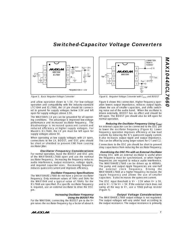
When operating at low supply voltages with LV open,connections to the LV, BOOST, and OSC pins shouldbe short or shielded to prevent EMI from causing oscillator jitter.
Oscillator Frequency ConsiderationsFor normal operation, leave the BOOST and OSC pinsof the MAX1044/ICL7660 open and use the nominaloscillator frequency. Increasing the frequency reducesaudio interference, output resistance, voltage ripple,and required capacitor sizes. Decreasing frequencyreduces quiescent current and improves efficiency.
Oscillator Frequency Specifications The MAX1044/ICL7660 do not have a precise oscillatorfrequency. Only minimum values of 1kHz and 5kHz forthe MAX1044 and a typical value of 10kHz for theICL7660 are specified. If a specific oscillator frequencyis required, use an external oscillator to drive the OSCpin.
Increasing Oscillator FrequencyUsing the BOOST Pin
For the MAX1044, connecting the BOOST pin to the V+pin raises the oscillator frequency by a factor of about 6.
Figure 6 shows this connection. Higher frequency oper-ation lowers output impedance, reduces output ripple,allows the use of smaller capacitors, and shifts switch-ing noise out of the audio band. When the oscillator isdriven externally, BOOST has no effect and should beleft open. The BOOST pin should also be left open fornormal operation.
Reducing the Oscillator Frequency Using COSCAn external capacitor can be connected to the OSC pinto lower the oscillator frequency (Figure 6). Lower frequency operation improves efficiency at low loadcurrents by reducing the IC’s quiescent supply current.It also increases output ripple and output impedance.This can be offset by using larger values for C1 and C2.
Connections to the OSC pin should be short to preventstray capacitance from reducing the oscillator frequency.
Overdriving the OSC Pin with an External OscillatorDriving OSC with an external oscillator is useful whenthe frequency must be synchronized, or when higherfrequencies are required to reduce audio interference.The MAX1044/ICL7660 can be driven up to 400kHz.The pump and output ripple frequencies are one-halfthe external clock frequency. Driving theMAX1044/ICL7660 at a higher frequency increases theripple frequency and allows the use of smaller capacitors. It also increases the quiescent current.
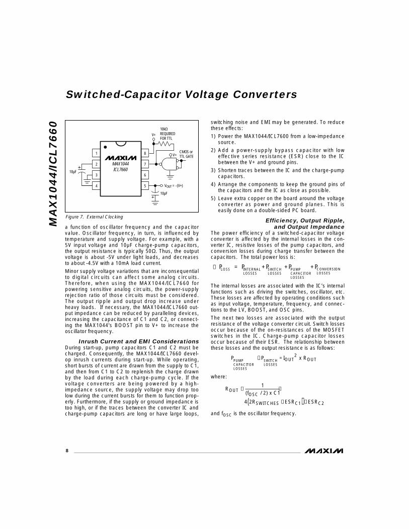
The OSC input threshold is V+ - 2.5V when V+ ≥ 5V,and is V+ / 2 for V+ < 5V. If the external clock does notswing all the way to V+, use a 10kΩ pull-up resistor(Figure 7).
Output Voltage ConsiderationsThe MAX1044/ICL7660 output voltage is not regulated.The output voltages will vary under load according tothe output resistance. The output resistance is primarily
MA
X1
04
4/IC
L7
66
0
Switched-Capacitor Voltage Converters
_______________________________________________________________________________________ 7
MAX1044 ICL7660
4
3
C1 10µF
*REQUIRED FOR V+ < 3.5V
VOUT = -(V+)
C2 10µF
V+
2
1
5
6
7
8
*
CBYPASS
Figure 5. Basic Negative Voltage Converter
MAX1044
4
310µF COSC
VOUT = -(V+)
10µF
V+
2
1
5
6
7
8
CONNECTION FROM V+ TO BOOST
Figure 6. Negative Voltage Converter with COSC and BOOST
MA
X1
04
4/I
CL
76
60
a function of oscillator frequency and the capacitorvalue. Oscillator frequency, in turn, is influenced bytemperature and supply voltage. For example, with a5V input voltage and 10µF charge-pump capacitors,the output resistance is typically 50Ω. Thus, the outputvoltage is about -5V under light loads, and decreasesto about -4.5V with a 10mA load current.
Minor supply voltage variations that are inconsequentialto digital circuits can affect some analog circuits.Therefore, when using the MAX1044/ICL7660 for powering sensitive analog circuits, the power-supplyrejection ratio of those circuits must be considered.The output ripple and output drop increase underheavy loads. If necessary, the MAX1044/ICL7660 out-put impedance can be reduced by paralleling devices,increasing the capacitance of C1 and C2, or connect-ing the MAX1044’s BOOST pin to V+ to increase theoscillator frequency.
Inrush Current and EMI ConsiderationsDuring start-up, pump capacitors C1 and C2 must becharged. Consequently, the MAX1044/ICL7660 devel-op inrush currents during start-up. While operating,short bursts of current are drawn from the supply to C1,and then from C1 to C2 to replenish the charge drawnby the load during each charge-pump cycle. If the voltage converters are being powered by a high-impedance source, the supply voltage may drop toolow during the current bursts for them to function prop-erly. Furthermore, if the supply or ground impedance istoo high, or if the traces between the converter IC andcharge-pump capacitors are long or have large loops,
switching noise and EMI may be generated. To reducethese effects:
1) Power the MAX1044/ICL7600 from a low-impedancesource.
2) Add a power-supply bypass capacitor with loweffective series resistance (ESR) close to the ICbetween the V+ and ground pins.
3) Shorten traces between the IC and the charge-pumpcapacitors.
4) Arrange the components to keep the ground pins ofthe capacitors and the IC as close as possible.
5) Leave extra copper on the board around the voltageconverter as power and ground planes. This is easily done on a double-sided PC board.
Efficiency, Output Ripple, and Output Impedance
The power efficiency of a switched-capacitor voltageconverter is affected by the internal losses in the con-verter IC, resistive losses of the pump capacitors, andconversion losses during charge transfer between thecapacitors. The total power loss is:
The internal losses are associated with the IC’s internalfunctions such as driving the switches, oscillator, etc.These losses are affected by operating conditions suchas input voltage, temperature, frequency, and connec-tions to the LV, BOOST, and OSC pins.
The next two losses are associated with the outputresistance of the voltage converter circuit. Switch lossesoccur because of the on-resistances of the MOSFETswitches in the IC. Charge-pump capacitor lossesoccur because of their ESR. The relationship betweenthese losses and the output resistance is as follows:
where:
and fOSC is the oscillator frequency.
R1
(f / 2) x C1
4 2R ESR ESR
OUTOSC
SWITCHES C1 C2
≅ +
+( ) +
P P I x ROUT2
OUT+ =
∑ P = P +P +P +P
Switched-Capacitor Voltage Converters
8 _______________________________________________________________________________________
MAX1044 ICL7660
4
310µF
VOUT = -(V+)
10µF
V+
V+
CMOS or TTL GATE
10kΩ REQUIRED FOR TTL
2
1
5
6
7
8
Figure 7. External Clocking
LOSS INTERNALLOSSES
SWITCHLOSSES
PUMPCAPACITORLOSSES
CONVERSIONLOSSES
PUMPCAPACITORLOSSES
SWITCHLOSSES
The first term is the effective resistance from theswitched-capacitor circuit.
Conversion losses occur during the transfer of chargebetween capacitors C1 and C2 when there is a voltagedifference between them. The power loss is:
Increasing Efficiency Efficiency can be improved by lowering output voltageripple and output impedance. Both output voltage rip-ple and output impedance can be reduced by usinglarge capacitors with low ESR.
The output voltage ripple can be calculated by notingthat the output current is supplied solely from capacitorC2 during one-half of the charge-pump cycle.
Slowing the oscillator frequency reduces quiescent cur-rent. The oscillator frequency can be reduced by con-necting a capacitor to the OSC pin.
Reducing the oscillator frequency increases the ripplevoltage in the MAX1044/ICL7660. Compensate byincreasing the values of the bucket and reservoircapacitors. For example, in a negative voltage converter,the pump frequency is around 4kHz or 5kHz. With therecommended 10µF bucket and reservoir capacitors,the circuit consumes about 70µA of quiescent currentwhile providing 20mA of output current. Setting the
oscillator to 400Hz by connecting a 100pF capacitor toOSC reduces the quiescent current to about 15µA.Maintaining 20mA output current capability requiresincreasing the bucket and reservoir capacitors to100µF.
Note that lower capacitor values can be used for loweroutput currents. For example, setting the oscillator to40Hz by connecting a 1000pF capacitor to OSC pro-vides the highest efficiency possible. Leaving the bucketand reservoir capacitors at 100µF gives a maximumIOUT of 2mA, a no-load quiescent current of 10µA, anda power conversion efficiency of 98%.
General Precautions1) Connecting any input terminal to voltages greater
than V+ or less than ground may cause latchup. Donot apply any input sources operating from externalsupplies before device power-up.
2) Never exceed maximum supply voltage ratings.
3) Do not connect C1 and C2 with the wrong polarity.
4) Do not short V+ to ground for extended periods withsupply voltages above 5.5V present on other pins.
5) Ensure that VOUT (pin 5) does not go more positivethan GND (pin 3). Adding a diode in parallel withC2, with the anode connected to VOUT and cathodeto LV, will prevent this condition.
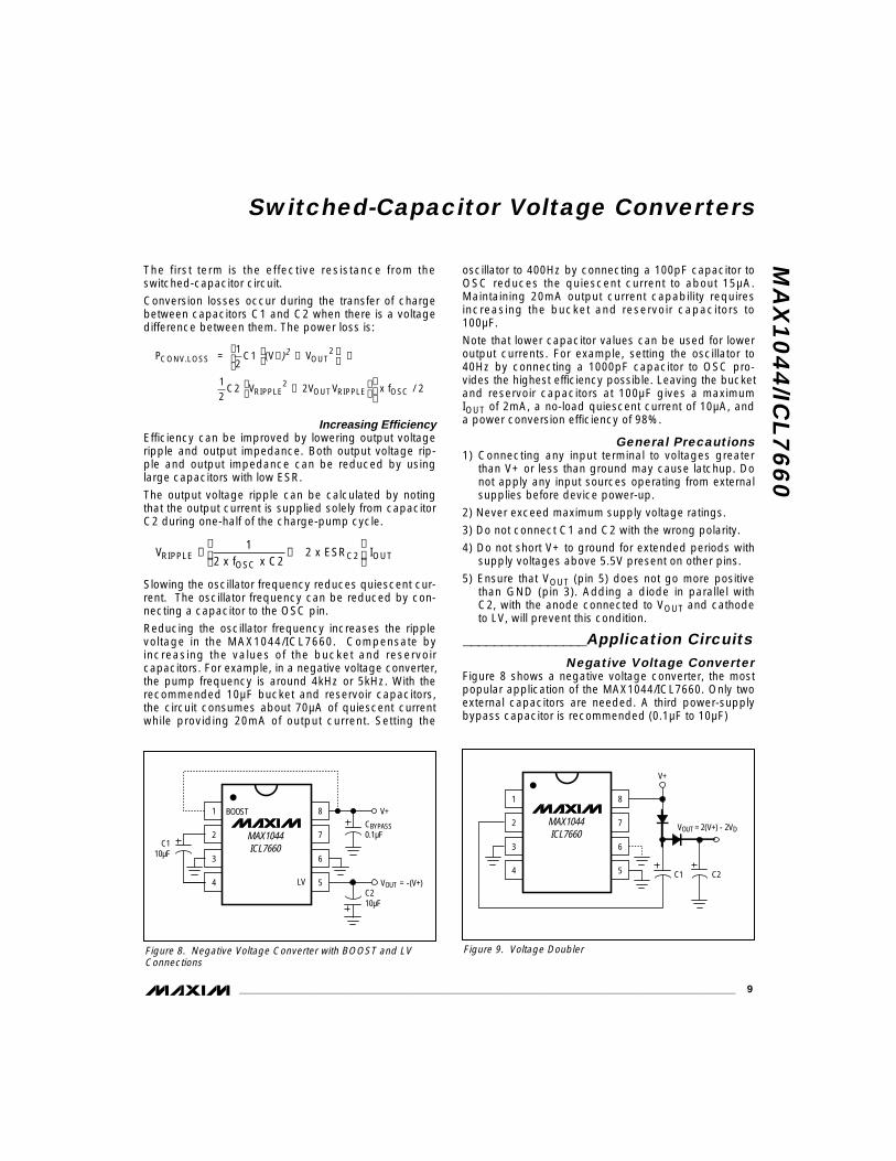
________________Application Circuits Negative Voltage Converter
Figure 8 shows a negative voltage converter, the mostpopular application of the MAX1044/ICL7660. Only twoexternal capacitors are needed. A third power-supplybypass capacitor is recommended (0.1µF to 10µF)
V1
2 x f x C2 2 x ESR IRIPPLE
OSCC2 OUT≅ +
P12
C1 (V V
12
C2 V 2V V x f / 2
CONV.LOSS OUT2
RIPPLE2
OUT RIPPLE OSC
)= + −
+
−
2
MA
X1
04
4/IC
L7
66
0
Switched-Capacitor Voltage Converters
_______________________________________________________________________________________ 9
MAX1044 ICL7660
4
3
C1 10µF
VOUT = -(V+)
CBYPASS 0.1µF2
1
5
6
7
8
C2 10µF
V+BOOST
LV
Figure 8. Negative Voltage Converter with BOOST and LVConnections
MAX1044 ICL7660
4
3
VOUT = 2(V+) - 2VD2
1
5
6
7
8
C1 C2
V+
Figure 9. Voltage Doubler
MA
X1
04
4/I
CL
76
60
Positive Voltage DoublerFigure 9 illustrates the recommended voltage doublercircuit for the MAX1044/ICL7660. To reduce the voltagedrops contributed by the diodes (VD), use Schottkydiodes. For true voltage doubling or higher output cur-rents, use the MAX660.
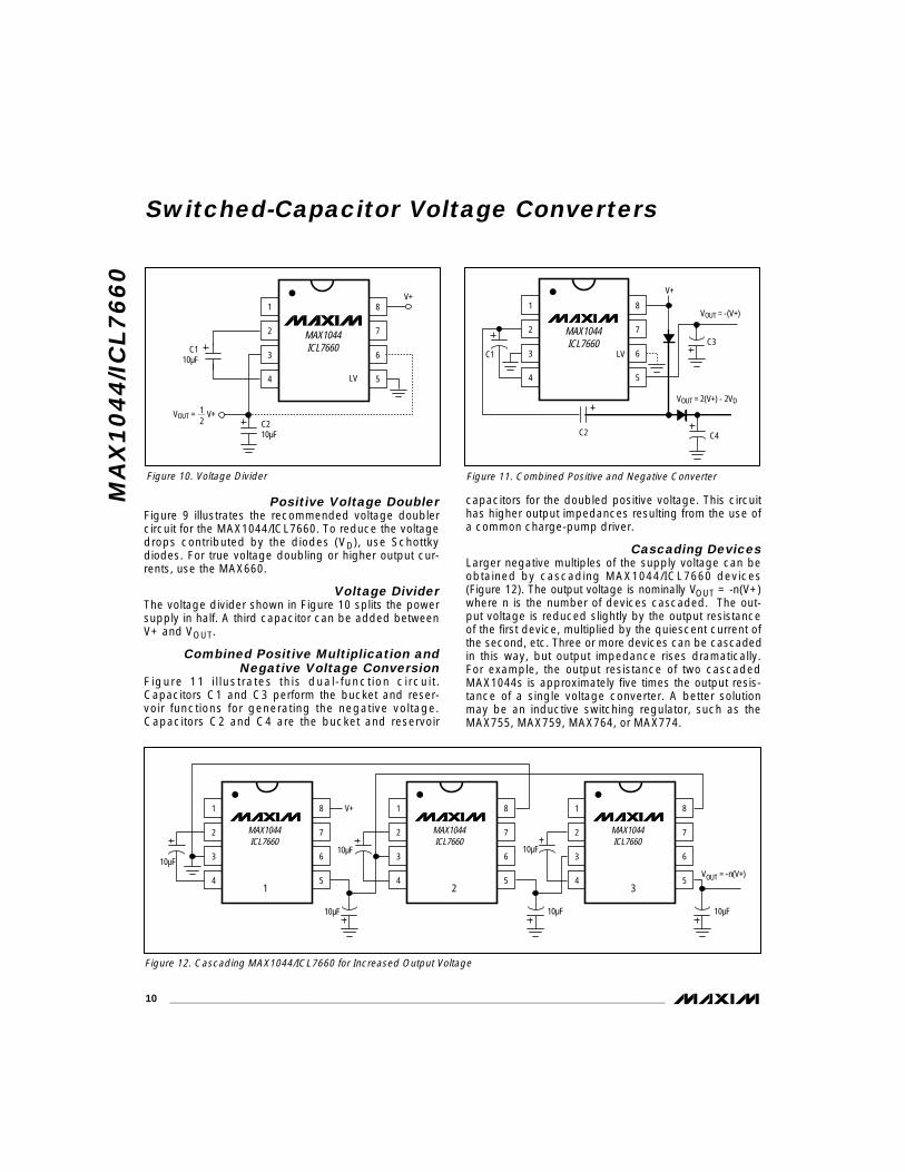
Voltage DividerThe voltage divider shown in Figure 10 splits the powersupply in half. A third capacitor can be added betweenV+ and VOUT.
Combined Positive Multiplication andNegative Voltage Conversion
Figure 11 i l lustrates this dual-function circuit.Capacitors C1 and C3 perform the bucket and reser-voir functions for generating the negative voltage.Capacitors C2 and C4 are the bucket and reservoir
capacitors for the doubled positive voltage. This circuithas higher output impedances resulting from the use ofa common charge-pump driver.
Cascading DevicesLarger negative multiples of the supply voltage can beobtained by cascading MAX1044/ICL7660 devices(Figure 12). The output voltage is nominally VOUT = -n(V+)where n is the number of devices cascaded. The out-put voltage is reduced slightly by the output resistanceof the first device, multiplied by the quiescent current ofthe second, etc. Three or more devices can be cascadedin this way, but output impedance rises dramatically.For example, the output resistance of two cascadedMAX1044s is approximately five times the output resis-tance of a single voltage converter. A better solutionmay be an inductive switching regulator, such as theMAX755, MAX759, MAX764, or MAX774.
Switched-Capacitor Voltage Converters
10 ______________________________________________________________________________________
MAX1044 ICL7660
4
3
2
1
5
6
7
8
C2 10µF
C1 10µF
V+
VOUT = V+12
LV
Figure 10. Voltage Divider
MAX1044 ICL7660
4
3
VOUT = 2(V+) - 2VD
2
1
5
6
7
8
C4
C1
C2
V+
VOUT = -(V+)
C3LV
Figure 11. Combined Positive and Negative Converter
MAX1044 ICL7660
4
3
2
1
5
6
7
8
MAX1044 ICL7660
4
3
2
1
5
6
7
8
10µF
10µF
V+
10µF
10µF
10µF
VOUT = -n(V+)
10µF
MAX1044 ICL7660
4
3
2
1
5
6
7
8
1 2 3
Figure 12. Cascading MAX1044/ICL7660 for Increased Output Voltage
Paralleling DevicesParalleling multiple MAX1044/ICL7660s reduces outputresistance and increases current capability. As illus-trated in Figure 13, each device requires its own pumpcapacitor C1, but the reservoir capacitor C2 serves alldevices. The equation for calculating output resistance is:
Shutdown SchemesFigures 14a–14c illustrate three ways of adding shut-down capability to the MAX1044/ICL7660. When usingthese circuits, be aware that the additional capacitiveloading on the OSC pin will reduce the oscillator fre-quency. The first circuit has the least loading on theOSC pin and has the added advantage of controllingshutdown with a high or low logic level, depending onthe orientation of the switching diode.
R R (of MAX1044 or ICL7660)
n (number of devices)OUTOUT=
MA
X1
04
4/IC
L7
66
0
Switched-Capacitor Voltage Converters
______________________________________________________________________________________ 11
MAX1044 ICL7660
4
3
VOUT = -(V+)
2
1
5
6
7
8
C2
C1
V+
MAX1044 ICL7660
4
3
2
1
5
6
7
8
C1
1
n
Figure 13. Paralleling MAX1044/ICL7660 to Reduce OutputResistance
MAX1044 ICL7660
4
310µF
VOUT = -(V+)
10µF
CMOS or TTL GATE
1N4148
V+
2
1
5
6
7
8V+
10kΩ REQUIRED FOR TTL
Figure 14a-14c. Shutdown Schemes for MAX1044/ICL7660
OUTPUT ENABLE 74HC126 OR 74LS126 TRI-STATE BUFFER
V+
7MAX1044 ICL7660
74HC03 OPEN-DRAIN OR 74LS03 OPEN-COLLECTOR NAND GATES
V+
MAX1044 ICL7660
7
a)
b)
c)
8 CERDIP**
8 SO
PIN-PACKAGETEMP. RANGE
-40°C to +85°C
-55°C to +125°CMAX1044MJA
MAX1044ESA
PART
8 Plastic DIP0°C to +70°CICL7660CPA8 SO0°C to +70°CICL7660CSA8 µMAX0°C to +70°CICL7660CUADice*0°C to +70°CICL7660C/D8 Plastic DIP-40°C to +85°CICL7660EPA8 SO-40°C to +85°CICL7660ESA8 CERDIP**-55°C to +125°CICL7660AMJA†
8 TO-99**-55°C to +125°CICL7660AMTV†
_Ordering Information (continued)
* Contact factory for dice specifications.** Contact factory for availability.† The Maxim ICL7660 meets or exceeds all “A” and “S”
specifications.
Maxim cannot assume responsibility for use of any circuitry other than circuitry entirely embodied in a Maxim product. No circuit patent licenses areimplied. Maxim reserves the right to change the circuitry and specifications without notice at any time.
12 __________________Maxim Integrated Products, 120 San Gabriel Drive, Sunnyvale, CA 94086 (408) 737-7600
© 1994 Maxim Integrated Products Printed USA is a registered trademark of Maxim Integrated Products.
MA
X1
04
4/I
CL
76
60
Switched-Capacitor Voltage Converters
__________________________________________________________Chip Topographies
GND
CAP-
LVVOUT
TRANSISTOR COUNT: 71 SUBSTRATE CONNECTED TO V+
CAP+0.084"
(2.1mm)
0.060" (1.5mm)
V+
OSC
ICL7660
GND CAP+ BOOST
0.076" (1.930mm)
0.076" (1.930mm)
CAP-
VOUT
V+
OSCLV
TRANSISTOR COUNT: 72 SUBSTRATE CONNECTED TO V+
MAX1044
L
αC
A1B
DIM
A A1 B C D E e H L α
MIN 0.036 0.004 0.010 0.005 0.116 0.116
0.188 0.016
0°
MAX 0.044 0.008 0.014 0.007 0.120 0.120
0.198 0.026
6°
MIN 0.91 0.10 0.25 0.13 2.95 2.95
4.78 0.41 0°
MAX 1.11 0.20 0.36 0.18 3.05 3.05
5.03 0.66 6°
INCHES MILLIMETERS
8-PIN µ MAX PACKAGE
0.650.0256
21-0036
A
e
E H
D
0.127mm 0.004 in
________________________________________________________Package Information


![cap11.ppt [Modo de Compatibilidade] - ufjf.br · O Amplificador Operacional Um amplificador operacional ou amp op é um amplificador com ganho muito elevado. Tem dois terminais de](https://img.document.onl/doc/110x75/5be1a4f309d3f280068b5dd7/cap11ppt-modo-de-compatibilidade-ufjfbr-o-amplificador-operacional-um.jpg)