Embed Size (px)
Citation preview

INVESTIGATION ON THE STRUCTURAL AND
OPTICAL PROPERTIES OF Alq3/METAL/Alq3 HYBRID
SANDWICH STRUCTURE FOR OLED APPLICATIONS
Thaiana Vale Smilgevicius
Projeto de Graduação apresentado ao
Curso de Engenharia de Materiais da
Escola Politécnica, Universidade Federal
do Rio de Janeiro, como parte dos
requisitos necessários à obtenção do
título de Engenheira de Materiais.
Orientadores: Prof. Renata Antoun Simão, DSc.
Prof. Vidhya Chavan, DSc.
Ing. Mohan Amalraj, MSc.
Rio de Janeiro
Julho de 201


iii
Smilgevicius, Thaiana Vale
Investigation on the Structural and Optical
Properties of Alq3/Metal/Alq3 Hybrid Sandwich
Structure for OLED Applications / Thaiana Vale
Smilgevicius. – Rio de Janeiro: UFRJ / Escola
Politécnica, 2018.
xiii, 50 p.: II; 29,7 cm.
Orientadores: Prof. Renata Antoun Simão, DSc., Prof.
Vidhya Bhavan, DSC., Ing. Mohan Amalraj. MSc.
Projeto de Graduação – UFRJ / Escola
Politécnica / Engenharia de Materiais, 2018.
Referências Bibliográficas: p. 45-50.
1. Sandwich Structure. 2. OLED 3. Physical Vapor
Deposition. I. Simão, Renata Autoun. II.
Universidade Federal do Rio de Janeiro, Escola
Politécnica, Curso de Engenharia de Materiais. III.
Investigation on the Structural and Optical
Properties of Alq3/Metal/Alq3 Hybrid Sandwich
Structure for OLED Applications.

iv
Acknowledgements
First and foremost, I thank my parents Vera Lúcia da S. V. Smilgevicius and
Otávio Luís Smilgevicius, my sister Vanessa Vale Smilgevicius and her
daughter Ana Clara, my uncles and my grandmothers for their unconditional
love and support throughout my life.
Even with cultural diversity, I chose to seek a differential for my academic
life and to acquire new knowledge. I found out about the IAEST program and I
have decided to register. In 2017 I was selected to participate in the program, in
Tamil Nadu, India. I would like to express my gratitude to the Karunya
University for providing necessary infrastructure and resources to accomplish
my research work. I thank the IAEST members for the internship opportunity.
This experience has made me a different person.
Thanks Federal University of Rio de Janeiro for renowned quality and
technology. It was a pleasure to study at one of the best university in Brasil.
I am thankful to my supervisor Renata Antoun Simão, in Federal University
of Rio de Janeiro, who has proved to be a great coordinator and an enabler
teacher. She always ready to help and teach all her students.
I pay homage to my supervisor Dr. B. Vidhya, in Karunya University. This
work would not have possible without her important guidance, innovative ideas,
comments and suggestions which made the project more interesting. I also
thank A. Mohan for the constant support, valuable explications and patience
throughout the project.
I would like to thank all professors in Federal University of Rio de Janeiro,
who were help to improve my studies. I can not forget the Vinay and Pranay
Kumar and their family, Sr. Alex, Isaac Nelson. P, S. Rajesh, Sheeba, Ashwini,
Judy, Vani, Amal, Adebisi and all my laboratory friends for make my internship
more agreeable.
Thank you Larissa Gôuvea and Olga Veridiano for being the best friends and
Jules Guépratte for joining me in these years.
To all my friends and for everyone, who directly or indirectly, contributed to
my formation as an engineer.

v
“Persistence is the
smallest phat to success.”
Charles Chaplin

vi
Resumo do Projeto de Graduação apresentado à Escola Politécnica/UFRJ como
parte dos requisitos necessários para a obtenção do grau de Engenheira de
Materiais.
INVESTIGATION ON THE STRUCTURAL AND OPTICAL
PROPERTIES OF Alq3/METAL/Alq3 HYBRID SANDWICH
STRUCTURE FOR OLED APPLICATIONS
Thaiana Vale Smilgevicius
Orientadores: Prof. Renata Antoun Simão, DSc., Prof. Vidhya Bhavan, DSC.,
Ing. Mohan Amalraj. MSc
Curso: Engenharia de Materiais
O Tris(8-hidroxiquinolinato) de alumínio (Alq3) é utilizado tanto na
camada de emissão como na camada de transporte de elétrons em diodos
orgânicos emissores de luz. (OLED).
Este trabalho contém resultados de investigação das propriedades
estruturais e ópticas de filmes finos de Alq3 comparados com a estrutura em
forma de sanduíche (Alq3 / Metal /Alq3), sendo os metais: Índio (In), Gálio (Ga),
Cobre (Cu) e Estanho (Sn); e depois comparado com o processo recozido da
estrutura (Alq3 / In /Alq3) a 150° C, 250° C e 350° C.
Esta estrutura em sanduíche foi preparada utilizando a técnica de
deposição física de vapor à temperatura ambiente. As espessuras das camadas
são de 50 nm e 30 nm respectivamente, para Alq3 e Metal.
As propriedades ópticas foram caracterizadas por emissão via
Fotoluminescência (PL) e Espectroscopia UV-Visível. As propriedades
estruturais foram analisadas por difração de raios X, Microscopia Eletrônica de
Varredura (MEV).
Os estudos de difração de raios X revelam a formação de compósitos.
Novas emissões de cores foram observadas na estrutura de sanduíche aquecida
e suas propriedades estruturais e ópticas foram melhoradas. Essas estruturas
multicamadas possuem amplas aplicações em dispositivos optoeletrônicos,
particularmente em OLEDs.
Palavras-chave: Alq3, Estrutura sanduíche, OLED, Deposição Física de Vapor

vii
Abstract of Undergraduate Project presented to POLI/UFRJ as a partial
fulfillment or the requirements for the degree of Materials Engineer.
INVESTIGATION ON THE STRUCTURAL AND OPTICAL
PROPERTIES OF Alq3/METAL/Alq3 HYBRID SANDWICH
STRUCTURE FOR OLED APPLICATIONS
Advisors: Prof. Renata Antoun Simão, DSc., Prof. Vidhya Bhavan, DSC., Ing.
Mohan Amalraj. MSc
Course :MaterialsEngineering
Tris- (8-hydroxyquinolinate) Aluminum (Alq3) is used both as the
emission and electron transport layer in organic light emitting diodes
(OLED).
This work contains results of investigation of the structural and optical
properties of Alq3thin films compared to sandwich (Alq3/ Metal Alq3)
structure being the metal Indium (In) (after compared with the its annealed
process (150o C, 250o C and 350o)), Gallium (Ga), Cooper (Cu) or Tin (Sn).
This sandwich structure was prepared using physical vapor deposition
technique at room temperature. The layers thickness is 50 nm and 30 nm
respectively for Alq3 and Metal. The photophysical properties were
characterized by emission via Photoluminescence (PL) and UV-Visible
Spectroscopy.
The structural properties were analyzed through X-ray diffraction,
Scanning Electron Microscopy (SEM). The X-ray diffraction studies reveal the
formation of composites. News colors emission was observed in the annealed
sandwich structure. The structural and optical properties were improved in
annealed hybrid sandwich structure. These type multilayer structures find ample
applications in optoelectronics devices particularly in OLEDs.
Keywords: Alq3, Sandwich Structure, OLED, Physical Vapor Deposition

viii
Summary of Contents
1. Introduction............................................................................................1
1.1. Aims..............................................................................................2
1.1.1. Specific Aims and Objective................................................2
2. Literature Review...................................................................................3
2.1. Tris (8-hydroxyquinoline) Aluminium (Alq3)..............................3
2.1.1. Structure of Alq3...................................................................3
2.1.2. Optical Properties of Alq3.....................................................4
2.1.3. Application of Alq3...............................................................5
2.2. Organic Light-Emitting Diodes (OLEDs)………………………5
2.3. Materials and Methods………………………………………….7
2.3.1. Importance of Alq3…………………………………………7
2.3.2. Properties and Application of Metals…………...…………8
2.3.2.1. Indium (In)…………………………………………8
2.3.2.2. Copper (Cu)……………..…………………………8
2.3.2.3. Gallium (Ga)…………………………………...…..9
2.3.2.4. Tin (Sn)………………………………………….....9
2.3.3. The Film Deposition…………………...…………………10
2.3.4. Physical Vapor Deposition (PVD)……………………..…11
2.3.4.1. PVD Working Principle………………………..…12
2.3.5. Selection of Materials…………………………………….13
2.3.6. Substrate Cleaning Process……………………………….14
2.3.7. Preparation of Alq3/Metal/Alq3 Hybrid Sandwich
Structure.…………………………………………...……….14
2.3.8. X-ray Diffraction Pattern…………………………………15
ix
2.3.8.1. Braggs Diffraction Law…………………………..15
2.3.8.2. Determination of Structural Parameters…………..16
2.3.9. Scanning Electron Microscopy………………...…………17
2.3.10. UV-Visible Spectroscopy……………………………...…18
2.3.11. Photoluminescence Spectroscopy………………………...20
3. Results and Discussion……………………………………………22
3.1. Enhancement of PL Emission Through Alq3 / Metal / Alq3
Hybrid Sandwich Structure With Different Metal Layers…………22
3.1.1. Experimental Details………………………………….....22
3.1.2. X-ray Diffraction…………………………………..…….23
3.1.3. Surface Morphological Analysis………………………....24
3.1.4. Optical Studies…………………………..………………..25
3.1.5. Partial Conclusion….……………………………………..29
3.2. Investigation on Structural and Optical Properties of Hybrid
Alq3/In/Alq3 Composite Thin Films…………………….........30
3.2.1. Experimental Details……………………………………...30
3.2.2. Structural Studies………………………………………....31
3.2.3. Surface Morphological Studies……...………………....…31
3.2.4. Optical Studies……………………………………………32
3.2.5. Partial Conclusion………………….……………………..36
3.3. Impact of Annealing on Hybrid Alq3 / In / Alq3
Composite Thin Films…………..…...……………………………36
3.3.1. Experimental Details……………………………………...36
3.3.2. Structural Studies…………………………………………37
3.3.3. Surface Morphological Studies…………………………...38
3.3.4. Optical Studies………………………………..…………..40
3.3.5. Partial Conclusion….……………………………………..43

x
4. Final Conclusion.……………………………………………………43
5. Suggestions for Future Studies……………………………………...44
6. Bibliographic References……………………………………………44
List of Figures
Figure 1 - Structure of Tris (8-hydroxyquinoline) aluminium (Alq3)[1]
Figure 2 - Light Emission [2]
Figure 3 - Organic light emitting diode [3]
Figure 4 - Schematic diagram of OLED device structure [4]
Figure 5 - Thermal evaporation unit
Figure 6 - HINDHIVAC Vacuum Chamber model 12A4D,
Figure 7 - Schematic diagram of Alq3/metal/Alq3 hybrid structure
Figure 8 - Schematic representation of Briggs’s Law [5]
Figure 9 - Ultraviolet-visible (UV-vis) spectroscopy working process [6]
Figure 11 - PL Spectrometer working setup [7]
Figure 10 - PL absorption and emission process [8]
Figure 12- Schematic diagram of Alq3/metal/Alq3 hybrid structure (a)
Alq3/Cu/Alq3 , (b) Alq3/Ga/Alq3, (c) Alq3/In/Alq3 and (d) Alq3/Sn/Alq3
Figure 13 - X-ray diffraction pattern of hybrids structures
Figure 14 - SEM image of Alq3/metal/Alq3 hybrid structure (a)
Alq3/Cu/Alq3, (b) Alq3/Ga/Alq3, (c) Alq3/In/Alq3 and

xi
(d) Alq3/Sn/Alq3
Figure 15 - Optical spectra of (a) as deposited Alq3and Alq3/metal/Alq3
hybrid structure (b) Alq3/Cu/Alq3 , (c) Alq3/Ga/Alq3, (d) Alq3/In/Alq3 and
(e) Alq3/Sn/Alq3
Figure 16 - Optical energy band gap of (a) as deposited Alq3and
Alq3/metal/Alq3 hybrid structure (b) Alq3/Cu/Alq3 ,
(c) Alq3/Ga/Alq3, (d) Alq3/In/Alq3 and (e) Alq3/Sn/Alq3
Figure 17 - PL emission spectra of (a) as deposited Alq3and Alq3/metal/Alq3
hybrid structure (b) Alq3/Cu/Alq3 (c) Alq3/Ga/Alq3, (d) Alq3/In/Alq3 and (e)
Alq3/Sn/Alq3
Figure 18 - Structure of hybrid sandwich (Alq3/In/Alq3)
Figure 19 - X-ray diffraction pattern, (a) Alq3 and (b) Alq3/In/ Alq3 hybrid
structure
Figure 20 - SEM images (a) Alq3and (b) Alq3/In/Alq3 hybrid structure
Figure 21 - Optical spectra of as deposited Alq3 and Alq3/In/Alq3 hybrid
structure (a) transmission and (b) absorption spectra
Figure 22 - Optical energy band gap (a) Alq3 and (b) Alq3/In/Alq3 hybrid
structure
Figure 23 - PL emission spectra (a) Alq3 and (b). Alq3/In/Alq3 hybrid
structure
Figure 24 - Alq3/In/Alq3 hybrid sandwich structure
Figure 25 - X-ray diffraction pattern of hybrid sandwich structure (a) as
deposited, (b)150°C, (c) 250°C and (d) 350°C
Figure 26 - SEM image of Alq3/In/ Alq3 hybrid structure with different
annealing temperatures
Figure 27 - Optical absorption spectra of of Alq3/In/ Alq3 hybrid structure
with different annealing temperatures

xii
Figure 28 - Optical energy band gap of Alq3/In/ Alq3 hybrid structure with
different annealing temperatures
Figure 29 - PL emission spectra of Alq3/In/Alq3 hybrid structure with
different annealing temperatures
List of Tables
Table 1 - Fundamental properties of different metals [9]
Table 2 - Physical vapor deposition unit specification (HHV – 12A4D)
Table 3 - XRD characteristic of hybrid structure
Table 4 - XRD characteristic of hybrid structure
List of Symbols and Abbreviations
D Grain size
Wavelength
β Full width at half maximum
δ Density
Micro strain
θ Bragg’s angle
k Excitation coefficient
T Transmission of film
Absorption coefficient
hυ Incident photon energy
Eg Optical energy band gap
B Constant

xiii
n Direct or indirect allowed transition coefficient
g Grams
Alq3 Tris (8-hydroxyquinoline) aluminium
In Indium
Cu Copper
Ga Gallium
Sn Tin
N Nitrogen
O Oxygen
mer Meridional
fac Facial
OLED Organic light-emitting diode
ETM Electron-transport material
ELM Emitting layer material
PVD Physical vapor deposition
XRD X-ray diffraction
SEM Scanning electron microscopy
UV Ultraviolet
PL Photoluminescence

1
1 Introduction
An organic light-emitting diode (OLED) is a light emitting diode (LED) with
an organic semiconductor layer located between two electrodes
(electroluminescent emission layer) and are composed of thin films which can
create light with the application of electricity and use less power and it can have
a brighter display than the LEDs or liquid crystal displays (LCDs). [10]
Conducting polymers has a great interest in research focus due to their
potential application such as optoelectronics, OLED displays, flexible solar
cells, etc. The OLEDs are used on digital displays of devices such as televisions,
computer monitors, cell phones, etc and it can be deposited on flexible surfaces.
Tris-(8-hydroxyquinoline) aluminum (Alq3) is an organometallic, compound
containing at least one bond between a carbon atom of an organic compound
and a metal and it has an important property of emitting light over different
wavelengths in the visible spectra.
The Alq3 is one of the materials which is the most commonly used in
molecular organic light emitting diodes (OLEDs), specifically used as electron
transport layer or emissive layer. Considerable works have been done to
improve the device performance and stability and each research is a step
towards the advancement of material science.[11, 12]
In the present study, a sandwich layer was produced by physical vapor
deposition technique (PVD) at room temperature and was investigate the
structural and optical properties of Alq3 thin films compared to sandwich
(Alq3/Metal/Alq3) structure being the metal Indium, Gallium (Ga), Cooper (Cu)
and Tin (Sn). The Indium deserved a better attention and because that, annealed
sandwich Alq3/In/Alq3 structures were studies.
Metals peaks were revealed through X-ray diffraction and the grain size was
calculated. The sandwich structure was analyzed by SEM image showing the
thin films surfaces and their morphological studies. The transmission and
absorption optical was produce by Ultraviolet-visible (UV-Vis) spectroscopy
and the optical energy band was calculated. Finally, a Photoluminescence (PL)
emission spectra was studied the optical properties. The results were analyzed
and discussed to come a descriptive conclusion.

2
1.1 Aims
The main goal of this work was to produce, obtain and characterize
the structural, optical and morphologically properties of a composite
Structure formed by the Tris (8-hydroxyquinoline) aluminium (Alq3) in form
of powder and a metal. Metals were chosen as Indium (In), Copper (Cu),
Gallium (Ga) or Tin (Sn) and they were deposited by Physical Vapor
Deposition (PVD) over the glass substrate. The samples Alq3/In/Alq3 were
annealed at different temperatures (150o C, 250o C and 350o) and their
properties compared.
The purpose of the study is the investigation these sandwich structures
and find applications in optoelectronics devices particularly in OLEDs.
1.1.1 Specific Aims and Objectives
In order to achieve the objective, the following work elements have been
set.
• Preparation of Alq3/Metal/Alq3 hybrid sandwich structure with different
metal layers such as Cu, In, Ga and Sn.
• Preparation of Alq3/In/Alq3 hybrid sandwich structure and to investigate
structural and optical properties.
• Preparation of Alq3/In/Alq3 hybrid sandwich structure and to investigate
the impact of annealing with different temperatures.
• The research findings are analysed through the characterizations of the
samples using XRD, SEM, optical absorption spectra and
photoluminescence.

3
2 Literature Review
2.1 Tris (8-hydroxyquinoline) Aluminium(Alq3)
2.1.1 Structure of Alq3
The tris (8-hydroxyquinoline) aluminium (Alq3) has the formula
Al(C9H6NO)3 , and it is an organometallic, compound containing at least one
bond between a carbon atom of an organic compound and a metal. The Alq3
density is 459.43 g/mol. A binder arrangement may give rise to optical isomers.
The octahedral complexes of the type MN3O
3, where M is a trivalent metal and
N and O stand for the nitrogen and oxygen atoms in the quinolone ligands, can
exhibit two different geometric isomers: meridional and facial.[13,14]
The figure 1 shows the different isomers of Alq3 which are related to the
crystalline phases, α-, β-, γ-, δ- and ε-. It is known that the isomeric state of α-
and β- have two mer-Alq3 molecules in a unit cell, while δ- have four fac-Alq3
per unit cell. Between the both forms, the meridional isomers are the dominant
form both in amorphous films and crystals of Alq3.[15,16]
Figure 1- Structure of Tris (8-hydroxyquinoline) aluminium (Alq3)
The different HOMO and LUMO levels predicted for the two isomers
influences the injection barrier and could act as traps for charge carriers. The
energy separation between the both is determined by the material bonding
structure. After external excitation, the electrons of atoms gain enough energy

4
and jump from HOMO level, the highest occupied molecular orbit to the LUMO
level, the lowest unoccupied molecular orbit.[17]
2.1.2 Optical Properties of Alq3
Theoretically, linear and nonlinear optical properties of the organometallic
compounds are similar to organic materials though the intensity of the nonlinear
response is higher. The Alq3 has an important property: The organic material
can emit light. It can be observed over different wavelengths in the visible
spectra. Green, blue and red colors are obtained from Alq3 and thereby the white
is acquired. The relationship between structures and light emission is decisive
to control the spectral yield of electro-luminescent devices. The Alq3 isomeric
states are an important parameter to relate the colors. For example, the green
emission is caused by a mer-isomer, while the blue emission is caused by a fac-
isomer.
The value of band gap Eg defines the fundamental light absorption edge
and because of that, this optical parameter is also important to be considered.
The light with enough energy can stimulate electrons from the highest occupied
molecular orbital (HOMO) to the lowest unoccupied molecular orbital
(LUMO). A small band gap is desire for the electron can walk a short way.
Figure 2 - Light Emission

5
The absorption and emission in Alq3 may happen due to electron transitions
between the both orbitals[18-21].
The first report on blue luminescent Alq3 obtained by a simple annealing
process from yellowish-green Alq3 (𝛂-phase), above the phase transition at
about 380 °C as the 𝛅-phase[31]. The figure 2 exemplify the organic material
light emission.
2.1.3 Applications of Alq3
The low molecular weight and conjugated organic materials constitute a big
field for the flat panel display technology. Hybrid organic-inorganic
nanocomposite materials can change the properties as the chemical resistance,
thermal stability, electrical and optical properties. These materials offer a wide
range of possibilities for preparing tailor-made materials and several advantages
for new optical applications. Tris(8-hydroxyquinoline)aluminum has become
the most widely used electroluminescent materials in organic light-emitting
diodes (OLED), solar cells and organic field- effect transistors (OFET)[22]. The
most important is the OLED, because the Alq3 can be used as electron-transport
material (ETM) for the ability to have good electron injection a high electron
mobility. The ETMs are utilized to accept electrons from cathode efficiently.
The other application, inside the OLED is emitting layer material (ELM) that
consists of light-emitting dyes or dopants dispersed in a suitable host material.
Other Alq3 advantages include the high thermal stability, high quantum
yield, even in the solid state and the formation of stable and pinhole-free thin
films. Alq3 serves as host material for various dyes to tune the emission color
from green to red[23,24].
2.2 Organic Light-Emitting Diodes (OLEDs)
Organic materials have previously been considered for the fabrication of
practical electroluminescent (EL) devices. There is a large number of organic
materials known to have extremely high fluorescence quantum efficiencies in
6
the visible spectrum[25,26].
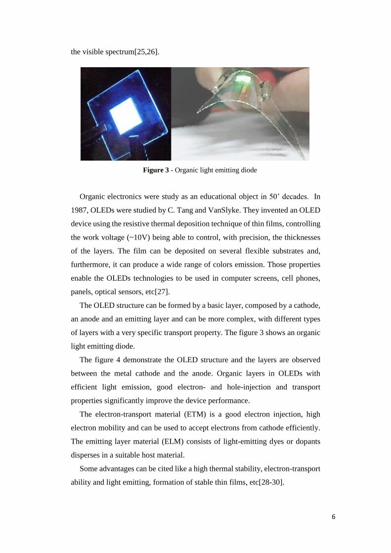
Figure 3 - Organic light emitting diode
Organic electronics were study as an educational object in 50’ decades. In
1987, OLEDs were studied by C. Tang and VanSlyke. They invented an OLED
device using the resistive thermal deposition technique of thin films, controlling
the work voltage (~10V) being able to control, with precision, the thicknesses
of the layers. The film can be deposited on several flexible substrates and,
furthermore, it can produce a wide range of colors emission. Those properties
enable the OLEDs technologies to be used in computer screens, cell phones,
panels, optical sensors, etc[27].
The OLED structure can be formed by a basic layer, composed by a cathode,
an anode and an emitting layer and can be more complex, with different types
of layers with a very specific transport property. The figure 3 shows an organic
light emitting diode.
The figure 4 demonstrate the OLED structure and the layers are observed
between the metal cathode and the anode. Organic layers in OLEDs with
efficient light emission, good electron- and hole-injection and transport
properties significantly improve the device performance.
The electron-transport material (ETM) is a good electron injection, high
electron mobility and can be used to accept electrons from cathode efficiently.
The emitting layer material (ELM) consists of light-emitting dyes or dopants
disperses in a suitable host material.
Some advantages can be cited like a high thermal stability, electron-transport
ability and light emitting, formation of stable thin films, etc[28-30].

7
Figure 4 - Schematic diagram of OLED device structure
2.3 Materials and Methods
2.3.1 Importance of Alq3
Recently, conducting polymers and polymer-based devices has a greater
interest in research focus due to their potential application such as
optoelectronics, organic light emitting diode (OLED) displays, flexible solar
cells, etc. [32-34] It is well-known that inorganic semiconductors when reduced
to the nanometer regime possess characteristics between the classic bulk and
molecular descriptions, exhibiting properties of quantum confinement. Thus,
adding metallic, semiconducting and dielectric nanocrystals into polymer
matrices enables the enhancement of efficiency and service duration of the
devices[35,36].
The inorganic additives usually were nanoparticles. The influence of
nanocrystalline oxides on the properties of semiconducting polymers has been
largely investigated by many groups [37,38]. It has been found that
nanostructured composites and nanohybrid layers or heterojunctions can be
applied to a variety of practical purposes.
Among these applications, two main directions have been set: one is focused
on the interaction between electrons and photons in devices such as OLEDs,
where the electricity generates light and the other aim at the generation of
8
electricity as in organic solar cells (OSCs). Tris-(8-hydroxyquinolinate)
aluminum (Alq3) is used both as the emission and electron transport layer in
organic light emitting diodes (OLED).
2.3.2 Properties and Application of Metals
2.3.2.1 Indium (In)
It was discovered by German chemists Ferdinand Reich and Hieronymus
Theodor Richter while they were examining zinc ore samples om 1863. A soft,
silvery metal that is stable in air and water. Most indium is used to make indium
tin oxide (ITO), which is an important part of touch screens, flat screen TVs and
solar panels. This is because it conducts electricity, bonds strongly to glass and
is transparent. Traditionally it has been one of the metals used to make coins,
along with silver and gold. However, it is the most common of the three and
therefore the least valued.[39]
2.3.2.2 Copper (Cu)
Copper was discovered by the ancients. The reddish-gold metal is easily
worked and drawn into wires. Most copper is used in electrical equipment such
as wiring and motors. This is because it conducts both heat and electricity very
well and can be drawn into wires. It also has uses in construction (for example
roofing and plumbing), and industrial machinery (such as heat exchangers).
Copper sulfate is used widely as an agricultural poison and as an algicide in
water purification. Copper compounds, such as Fehling’s solution, are used in
chemical tests for sugar detection[40].
2.3.2.3 Gallium (Ga)
Gallium was discovered by Paul-Émile Lecoq de Boisbaudran in 1875. It is

9
very soft, silvery-white metal, similar to aluminum. Solid gallium is a blue-gray
metal with orthorhombic crystalline structure; very pure gallium has a stunning
silvery color. Gallium is solid at normal room temperatures, but similar to
mercury, cesium, and rubidium it becomes liquid when heated slightly. Solid
gallium is soft enough to be cut with a knife. It is stable in air and water; but it
reacts with and dissolves in acids and alkalis.
Gallium arsenide has a similar structure to silicon and is a useful silicon
substitute for the electronics industry. It is an important component of many
semiconductors. It is also used in red LEDs (light emitting diodes) because of
its ability to convert electricity to light. Solar panels on the Mars Exploration
Rover contained gallium arsenide. Gallium nitride is also a semiconductor. It
has properties that make it very versatile. It has important uses in Blu-ray
technology, mobile phones, blue and green LEDs and pressure sensors for touch
switches. Gallium readily alloys with most metals. It is particularly used in low-
melting alloys[41].
2.3.2.4 Tin (Sn)
Tin is soft, pliable metal. Below 13°C it slowly changes to a powder form
and it has many uses. It takes a high polish and is used to coat other metals to
prevent corrosion, such as in tin cans, which are made of tin-coated steel. Alloys
of tin are important, such as soft solder, pewter, bronze and phosphor bronze. A
niobium-tin alloy is used for superconducting magnets. Most window glass is
made by floating molten glass on molten tin to produce a flat surface. Tin salts
sprayed onto glass are used to produce electrically conductive coatings. The
most important tin salt used is tin(II) chloride, which is used as a reducing agent
and as a mordant for dyeing calico and silk. Tin oxide is used for ceramics and
gas sensors. Zinc stannate (Zn2SnO4) is a fire-retardant used in plastics. Some
tin compounds have been used as anti-fouling paint for ships and boats, to
prevent barnacles. However, even at low levels these compounds are deadly to
marine life, especially oysters [42].

10
The table 1 organizes some important properties of each metal mentioned
above.
Properties Indium (In) Copper (Cu) Gallium (Ga) Tin (Sn)
Group 13 11 13 14
Period 5 4 4 5
Block p d p P
Atomic
number 49 29 31 50
State at 20°C Solid Solid Solid Solid
Electron
configuration [Kr] 4d105s25p1 [Ar] 3d104s1 [Ar] 3d104s24p1 [Kr] 4d105s25p2
Melting point 156.60°C 1084.62°C 29.76°C 231.93°C
Boiling point 2027°C 2560°C 2229°C 2586°C
Density (g
cm−3) 7.31 8.96 5.91 7.29
Atomic mass 114.82 63.55 69.72 118.71
Appearance
Table 1 - Fundamental properties of different metals
2.3.3 Thin Film Deposition
The deposition techniques can be classified under two main categories: The
vapor deposition and chemical deposition. Each process has its parameters
which determines the deposition atmosphere, deposition rate and the substrate
temperature. These parameters ensure thin films with specific and high quality
properties for the microstructure and the morphology of a given material[43].
The chemical vapor deposition (CVD) is used to produce high quality and

11
high performance solid materials generally in the semiconductor industry. The
technique consists of a deposition coating on a substrate previously cleaned.
One or more volatile fluid precursors produces a chemical change, reacting
or/and decomposing on the substrate surface leaving a chemically deposited
coating.
The physical vapor deposition (PVD) is fundamentally used to produce thin
films coatings. The two most common techniques of PVD are Thermal
Evaporation and Sputtering. In the present work the samples were prepared by
thermal evaporation due to its versatility to prepare quality thin films. The
thermal evaporation technique has been described below. [44,45].
2.3.4 Physical Vapor Deposition (PVD)
One of the promising methods of PVD technique is thermal evaporation
approach. It is vacuum based technology. It can deposit thin film, which are
usually in the thickness range of angstroms to microns. Also, it is possible to
deposit a single material, or multiple materials in a layered structure. The
materials to be deposited can be pure atomic elements including both metals and
non-metals or can be molecules such as oxides and nitrides. The object to be
coated is referred to as the substrate and can be any of a wide variety of materials
such as: semiconductor wafers, solar cells, glass, metallic surface or many other
possibilities[46].
Thermal evaporation involves heating a solid material inside a high vacuum
chamber, taking it to a temperature which produces some vapor pressure. Under
the vacuum condition, even a relatively low vapor pressure is sufficient to raise
a vapor cloud inside the chamber. This evaporated material now constitutes a
vapor stream, which traverses the chamber and hits the substrate, sticking to it
as a coating or film. Since, in most cases, the material is heated to its melting
point and is liquid, it is usually located in the bottom of the chamber, often in
some sort of upright crucible. The vapor then rises above this bottom source,
and the substrates are held inverted in appropriate fixtures at the top of the
chamber. The surfaces intended to be coated are thus facing down toward the

12
heated source material to receive their vapor. Steps may have to be taken to
assure film adhesion, as well as control various film properties as desired.
Figure 5 - Thermal evaporation unit
Fortunately, evaporation system design can allow adjustability of a number
of parameters in order to give process engineers the ability to achieve desired
results for such variables as thickness, uniformity, adhesion strength, stress,
grain structure, optical or electrical properties, etc.[47]
The thermal evaporation unit utilized at work is shown in figure 5.
2.3.4.1 PVD Working Principle and Instrument Specifications
The thermal evaporation technique can be used to produce thin films
involving transfer of material on an atomic level. The model used is
HINDHIVAC Vacuum Chamber model 12A4D and it is shown in figure 6. The
instrument specifications are in the table 2

13
Figure 6 - HINDHIVAC Vacuum Chamber model 12A4D
Table 2 -Physical vapor deposition unit specification (HHV – 12A4D)
2.3.5 Selection of Materials
Source materials with good trace metal basis are essential one to prepare
high quality thin films by thermal evaporation technique. A high purity Cu, Sn
Electrical Supply 230 volt AC
Pirani Gauge Range 0.05 to 0.001 m.bar
Penning Gauge Range 10-4 – 10-6m.bar
Number of boat used in a time 2 boats
Deposition pressure range 10-5 – 10-6m.bar
Radiant heater 275°C (maximum) about 30 min
Substrate heater 500°C (maximum) about 30 min
Deposition rate (uniform coating ) 1-3 Å /Sec

14
in the form as an ingot, In, Ga and Tris(8-hydroxyquinoline) aluminium (Alq3)
the form metal powder were purchased from Alfa Aesar and Sigma Aldrich,
respectively, with 99.99% trace metal basis. These metals are used to prepare
Alq3/metal/Alq3 hybrid sandwich structures. Two individual molybdenum
boats (200 amp) were used to place the source materials as an evaporator to
prepare the sandwich structures. One of the main reasons for choosing thermal
evaporation is less expensive and does not require any kind of substrates like
sapphire. In this work, glass substrates were used to prepare both reference and
multilayer composite structures.
2.3.6 Substrate Cleaning Process
When the substrate is exposed to atmosphere its gets contaminated by
dispersant particles in the air and even gases. The very important and first step
in thin film deposition is the substrate cleaning. Clean glass substrates are
important to assure the removal all the residual impurities. Firstly, the
substrates are cleaned thoroughly with soup solution and subsequently with
acetone. After that, the substrates were ultrasonically treated for ten minutes and
kept in a hot air oven to evaporate the residues. The cleaned glass substrates
were as substrates in the PVD technique.
2.3.7 Preparation of Alq3/metal/Alq3 hybrid Sandwich
Structure
The hybrid Alq3/ metal/Alq3 composite structure were deposited over the
glass substrate using thermal evaporation technique as shown figure 7. The high
purity base materials were placed in molybdenum boat (Alq3) and tungsten
basket (Cu, In, Ga and Sn) separately. The distance between the source
materials to substrate is fixed (28 cm). Initially Alq3 was deposited on the
substrate with a thickness of 50 nm and then metals (Cu, In, Ga and Sn) were
deposited with 30 nm thickness. Again, 50 nm of Alq3 was deposited followed
by metal layer without breaking the vacuum. The final structure seems like

15
sandwich and is known as hybrid structure. The thicknesses of each layer were
controlled and rate of evaporation was maintained 1-3 Å/sec using an in-situ
quartz crystal monitor throughout experiments. The figure 7 below the
schematic diagram Alq3/metal/Alq3 hybrid structure is represented.
Figure 7- Schematic diagram of Alq3/metal/Alq3 hybrid structure
2.3.8 X-ray Diffraction Pattern
X-ray diffraction is a fundamental and powerful tool to study the structure of
materials. It is non-destructive and common method for uses in all fields of
science and technology especially in material science. It can provide clear
information about the phase, crystallographic unit cell and crystal structure,
crystallographic texture, crystalline size, macro-stress and micro strain. Also, it
is widely used to determine materials in the atomic scale. In this work, Cu Kα
source was used to study the structural properties with the help X-ray
Diffractometer (Shimadzu XRD-6000) and diffraction angle (2θ) ranging
between 0-90◦. [48, 49]
2.3.8.1 Braggs Diffraction Law
An X-ray which reflects from the surface of a substance has travelled less
distance than an X-ray which reflects from a plane of atoms inside the crystal.

16
The penetrating X-ray travels down to the internal layer, reflects and travels
back over the same distance before being back at the surface. The distance
travelled depends on the separation of the layers and the angle at which the X-
ray entered the material. For this wave to be in phase with the wave which
reflected from the surface it needs to have travelled a whole number of
wavelengths while inside the material. Bragg expressed this in an equation now
known as Bragg's Law, in the figure 8: [50]
Figure 8 - Schematic Representation of Braggs’s Law
When X-rays are scattered from a crystal lattice, peaks of scattered intensity
are observed which correspond to the following conditions:
1. The angle of incidence = angle of scattering.
2. The path length difference is equal to an integer number of wavelengths.
The condition for maximum intensity contained in Bragg's law above allow
us to calculate details about the crystal structure, or if the crystal structure is
known, to determine the wavelength of the x-rays incident upon the crystal.
2.3.8.2 Determination of Structural Parameters
The x-ray diffraction patterns data can be used to calculate the structural
parameters like average grain size, macrostrain, dislocation density and lattice

17
parameter. The average grain size (D) of sandwich films was calculated using
Scherer’s equation
D =0.94
βcosθ ……………………… (1)
Where is the wavelength of the X-ray beam used (Cu k = 1.54Å), 2θ is
the angle between the incident and scattered X-ray beam and β is the full width
at half maximum. The dislocation density (δ) and micro strain () developed in
multilayer film are calculated from the relations[51-53].
=1
D2…………………….…… (2)
= βcosθ/4 ………………….. (3)
2.3.9 Scanning Electron Microscopy (SEM)
The electrons are emitted from the cathode and are accelerated by an electric
field up to required energy. Then the electrons are focused and scanned by
magnetic lenses which works based on the Lorentz force. The beam scans each
point in the sample surface and the detectors above the sample collect the
information, usually generated by the secondary beam electrons. Focal length
can be modified by using magnetic lenses and the size of the beam spot.
The scan generator controls the electron beam scanning and the succession
of pixels on the screen. The main factors determining resolution are the size of
the beam on the sample surface, the energy escaped of the sample surface and
excited by the beam sample volume.
The scanning electron microscopy is perhaps the most routinely utilized
instrument for the characterization of nanomaterials. It is possible to obtain
secondary electron images of organic and inorganic materials with nano scale
resolution. It can be used for studying the surface topography, microstructure
and chemistry of metallic and non-metallic specimens at magnification from 50
up to ~ 100, 000 X, with a resolution limit < 10nm (down to ~ 1nm) and a depth
of focus up to several μm (at magnifications ~ 10, 000 X). The surface

18
morphological properties, size, shape was studied by using scanning electron
microscopy (SEM - Jeol). The elemental analysis of films was obtained by
energy-dispersive X-ray spectroscopy (EDXS - Oxford)[54].
2.3.10 UV-Visible Spectroscopy
The UV-Visible absorption experiment for samples as shown in figure 9 for
film samples, the mechanism is the same. A light is emitted from the lamp and
then it passes through a filter. A beam of monochromatic light is split into two
beams; one of them passes through the sample and the other passes through a
reference.
Figure 9 – UV-Visible Spectroscopy Working Process
After the light is transmitted over the sample and reference the two beams
are directed back to the detectors where they are compared. The difference
between the signals is then measured. The result of the measurement is shown
by a graph. [55]
Ultraviolet-visible (UV-vis) spectroscopy is widely utilized to quantitatively
characterize organic, inorganic, nanomaterials and thin films. A sample is
irradiated with electromagnetic waves in the ultraviolet and visible ranges and
the absorbed light is analyzed through the resulting spectrum. It is not only used
for characterization, but also for sensing applications. The samples can be either

19
organic or inorganic, and may exist in gaseous, liquid or solid form. Different
sized materials can be characterized, ranging from transition metal ions and
small molecular weight organic molecules, whose diameters can be several, to
nano-particles and bulk materials. Size dependent properties can also be
observed Ångstroms in a UV-visible spectrum, particularly in the nano and
atomic scales. These include peak broadening and shifts in the absorption
wavelength.
Many electronic properties, such as the band gap of a material, can also be
determined by this technique. Optical absorption and transmission spectra was
recorded using UV-VIS-NIR spectrophotometer (Jasco-570 UV/VIS/ NIR
Spectrophotometer) in the range of 200 to 2500 nm. The absorption and
excitation coefficient were calculated from the following the relations:
k = ln(
1
T)
4t…………………. (4)
= 4k
…………………… (5)
Here k is an excitation coefficient, λ is an incident wavelength and T is
transmission of film, t is thickness of film and α is an absorption coefficient.
Most of the semiconductors especially chalcogenide follows an exponential law
and the absorption coefficient could be obeying the given equation
(αhυ)1
n = B (hυ − Eg) …………….. (6)
Where α is absorption coefficient, hυ is incident photon energy, B is a
constant, Eg is the optical energy band gap and n is an exponent constant. For,
the band gap of semiconductor follows the Fermi golden rule of direct (n = ½)
and indirect (n = 2) allowed transition for fundamental band-to-band electronic
transitions. Therefore, the optical energy band gap (Eg) can be expressed
following relation: [56,57]
(αhυ)2 = B (hυ − Eg) …………….. (7)

20
2.3.11 Photoluminescence Spectroscopy
PL spectroscopy concerns monitoring the light emitted from atoms or
molecules after they have absorbed photons. PL spectroscopy is suitable for the
characterization of both organic and inorganic materials of virtually any size,
and the samples can be in solid, liquid, or gaseous forms. Electromagnetic
radiation in the UV and visible ranges is utilized in PL spectroscopy. The figure
10 a simple scheme to exemplify the Spectrometer working setup.
The sample’s PL emission properties are characterized by four parameters:
intensity, emission wavelength, bandwidth of the emission peak and the
emission stability. The PL properties of a material can change in different
ambient environments, or in the presence of other molecules[58,59].
Many nanotechnology-enabled sensors are based on monitoring such
changes. Furthermore, as dimensions are reduced to the nanoscale, PL emission
properties can change, in particular a size dependent shift in the emission
wavelength can be observed. Additionally, because the released photon
corresponds to the energy difference between the states, PL spectroscopy can
be utilized to study material properties such as band gap, recombination
mechanisms and impurity levels.
Figure 10- PL Spectrometer working setup

21
Figure 10 - PL absorption and emission process
In a typical PL spectroscopy setup for liquid samples a solution containing
the sample is placed in a quartz cuvette with a known path length. Double beam
optics are generally employed. The first beam passes through an excitation filter
or monochromator, then through the sample and onto a detector. This impinging
light causes photoluminescence, which is emitted in all directions. A small
portion of the emitted light arrives at the detector after passing through an

22
optional emission filter or monochromator. A second reference beam is
attenuated and compared with the beam from the sample. Solid samples can also
be analyzed, with the incident beam impinging on the material (thin film,
powder etc.). the figure 10 shows the PL absorption and emission process.
Generally, an emission spectrum is recorded, where the sample is irradiated
with a single wavelength and the intensity of the luminescence emission is
recorded as a function of wavelength. The fluorescence of a sample can also be
monitored as a function of time, after excitation by a flash of light. This
technique is called time resolved fluorescence spectroscopy.
3 Results and Discussion
3.1 Enhancement of PL Emission Through Alq3 / Metal /
Alq3 Hybrid Sandwich Structure With Different Metal Layers
3.1.1 Experimental Details
The hybrid Alq3/Metal/Alq3 composite structure were deposited over the
glass substrate using thermal evaporation technique at ambient temperature as
shown in Figure 12. The thicknesses of each layer were controlled and rate of
evaporation was maintained at 1-3 Å/sec using an in-situ quartz crystal monitor.
After that all the films were taken for structural, optical and morphological
studies.
Figure 12 - Schematic diagram of Alq3/metal/Alq3 hybrid structure (a) Alq3/Cu/Alq3 ,
(b) Alq3/Ga/Alq3, (c) Alq3/In/Alq3 and (d) Alq3/Sn/Alq3

23
3.1.2 X-Ray Diffraction
Figure 13 shows the XRD pattern of as deposited Alq3/metal/Alq3 hybrid
structure with different metal layers. There is no significant peak found for as
deposited Alq3 [60]. All the samples have single diffraction peak at different 2θ
value and which indicates the presence of metal layers. The diffraction peaks
observed at 32.77, 42.88, 30.10 and 23.67° corresponds to (111), (020), (200)
and (101) planes respectively. Which is characteristic peak of Cu, Ga, In and
Sn.
10 20 30 40 50 60
(101)
(200)
(020)
(e).Alq3/Sn/Alq
3
(d).Alq3/In/Alq
3
(c).Alq3/Ga/Alq
3
(b).Alq3/Cu/Alq
3
(a). Alq3
Inte
ns
ity
(a
.u)
2 (deg)
(111)
Figure 13 - X-ray diffraction pattern of hybrids structures
Table 3 shows the XRD characteristic of hybrid sandwich structure for its d-
spacing, grain size and dislocation density. The grain size (D) was calculated
using Scherer’s equation [61,62].

24
Sample /
parameter
2θ
(deg)
FWHM
(deg)
D
(nm)
( )
X 10-22 (nm-2)
X 10-3
AIA 32.77 0.76 11 0.83 3.20
ACA 42.88 0.84 10.5 9.90 7. 30
AGA 30.10 3.00 3 10.40 11.21
ASA 23.67 1.30 6.5 2.35 5.08
Table 3 - XRD characteristic of hybrid structure
3.1.3 Surface Morphological Analysis
Figure 14 -SEM image of Alq3/metal/Alq3 hybrid structure (a) Alq3/Cu/Alq3 ,
(b) Alq3/Ga/Alq3, (c) Alq3/In/Alq3 and (d) Alq3/Sn/Alq3
a) b)
c) d)

25
Figure 14 shows the surface morphology of Alq3/metal/Alq3 hybrid structure.
The non- homogenous surface with rod like structure was observed for
Alq3/Cu/Alq3 as shown in figure 14.a. The mixed surface of rod and
nanocrystals was observed for Alq3/Ga/Alq3. Uniform spherical grains was
spread over the entire surface on which rod like structure appreared for
Alq3/In/Alq3 .
The non-homogenous hollow like shape was observed for Alq3/Sn/Alq3.
From the SEM images, it is clear that metal layer play vital role in surface
morphology due to variation in grain size.
It is important to observe the image shows only the deposition of Alq3 on the
metal and. The metal covers all the bottom layer. When the indium metal is
deposited over the polymeric surface, distinct grains were evident and definite
particles were seen on the surface.
3.1.4 Optical Studies
Figure 15 shows the optical absorption spectra of the Alq3/metal/Alq3 hybrid
structure with different metal layers. Strong absorption was observed in UV-
Visible region and higher transmission in infrared region.
There are two absorption peaks almost near 300 nm and 390 nm for all the
samples. The absorption edge was found at 393 nm and red-shift was observed
for Alq3/In/Alq3 hybrid structure compared to other structures. This is mainly
due to large grains size which is evident in XRD pattern.
Figure 15.a shows the optical transmission spectra of the Alq3/metal/ Alq3
hybrid structure with different metal layers. As deposited Alq3 films has higher
transmission than hybrid structures. The transmission was reducing due to
sandwiching metal layers. It is very interesting to state that metal layers play
very important role in sandwich structure.
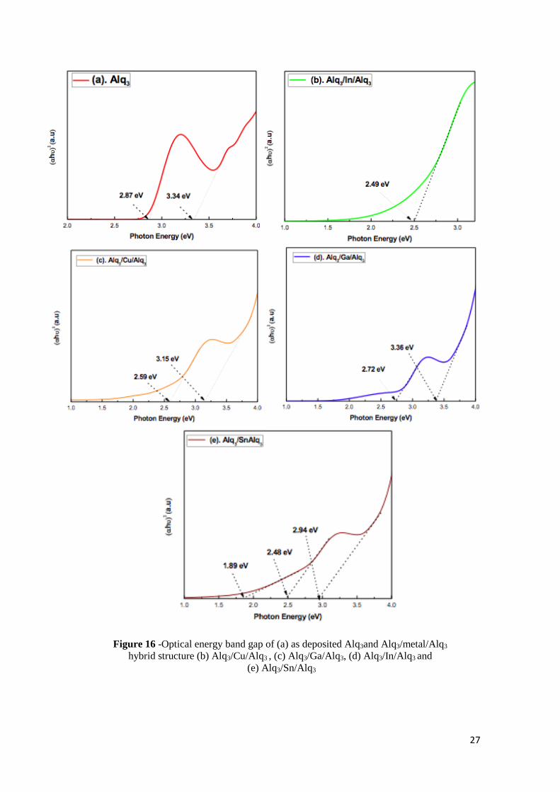
Figure 16 shows the optical band energy for Alq3/metal/Alq3 hybrid structure
with different metal layers. A couple of energy band was observed for almost
all samples. The estimated values were found to be between 1.92 and 3.36 eV.
A single band gap value found at 2.48 eV for Alq3/In/Alq3 hybrid structure
because only the π-π* electronic excitation is evident while in Alq3 UV-Vis

26
shows two electronic transitions [63]. The Alq3/Cu/Alq3 hybrid structure have
two band gaps at 2.59 and 3.15 eV as shown in figure 16.
500 1000 1500 2000 2500
Tra
ns
mis
sio
n (
a.u
)
Wavelength (nm)
(a). Alq3
(b). ACA
(c). AGA
(d). AIA
(e). ASA
300 400 500 600 700 800 900 1000
Ab
so
rpti
on
(a
.u)
Wavelength (nm)
(a). Alq3
(b). ACA
(c). AGA
(d). AIA
(e). ASA
Figure 15 -Optical spectra (Transmission a) and Absorption b)) of (a) as
deposited Alq3and Alq3/metal/Alq3 hybrid structure (b) Alq3/Cu/Alq3 ,
(c) Alq3/Ga/Alq3, (d) Alq3/In/Alq3 and (e) Alq3/Sn/Alq3
a)
b)
27
Figure 16 -Optical energy band gap of (a) as deposited Alq3and Alq3/metal/Alq3
hybrid structure (b) Alq3/Cu/Alq3 , (c) Alq3/Ga/Alq3, (d) Alq3/In/Alq3 and
(e) Alq3/Sn/Alq3
28
The band gap values were found to 2.72 and 3.36 eV for Alq3/Ga/Alq3, which
is wider than another hybrid structure. This increase in the optical band gap can
be related to formation of nanocrystal and rod like shapes for Alq3/Ga/Alq3
hybrid structure.
Three band values were found at 1.89, 2.48, 2.94 eV due to hollow shapes,
which leads to optical splitting for Alq3/Sn/Alq3 hybrid structure. The band gap
splitting due to nanocrystal formation and there can be possiblilty for more than
one band-to-band electronic transitions. The phenomena is mainly due to spin-
orbit split of the valence band. The blue shift, optical splitting and increasing in
band gap is evident for confinement effect or quantum size effect.
450 500 550 600 650 700 750
PL
em
issi
on
(a.u
)
Wavelength (nm)
(a). Alq3
(b). ACA
(c). AGA
(d). AIA
(e). ASA
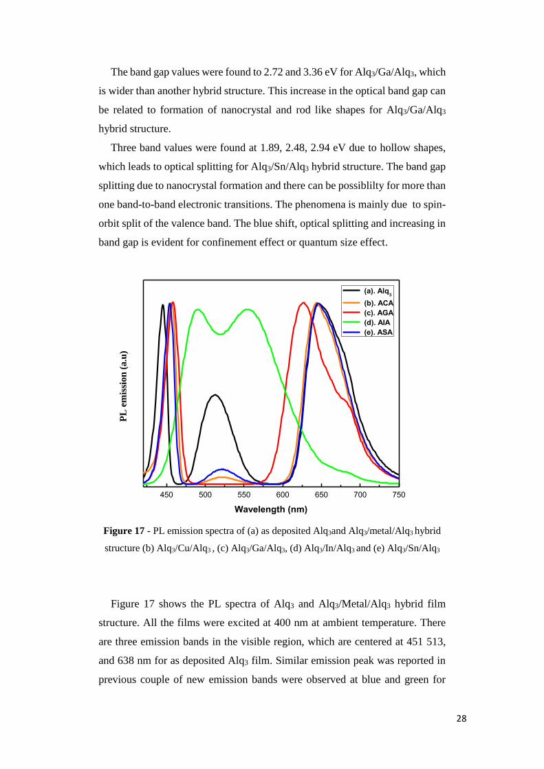
Figure 17 - PL emission spectra of (a) as deposited Alq3and Alq3/metal/Alq3 hybrid
structure (b) Alq3/Cu/Alq3 , (c) Alq3/Ga/Alq3, (d) Alq3/In/Alq3 and (e) Alq3/Sn/Alq3
Figure 17 shows the PL spectra of Alq3 and Alq3/Metal/Alq3 hybrid film
structure. All the films were excited at 400 nm at ambient temperature. There
are three emission bands in the visible region, which are centered at 451 513,
and 638 nm for as deposited Alq3 film. Similar emission peak was reported in
previous couple of new emission bands were observed at blue and green for

29
Alq3/In/Alq3 hybrid structure as shown in figure 17.b. The Alq3/Ga/Alq3 hybrid
structure having two emission, one is belonging to blue region and almost in red
region as seen in figure 17.c. Two emission bands were obtained at blue and
orange region for Alq3/Sn/Alq3 and Alq3/Cu/Alq3 hybrid structure.
The Cu and Sn sandwich has similar emission properties compared to other
sandwich structures. This is mainly due to the new composite formation and
impact of metal layer [60]. From the emission spectra, unique emission
properties were observed based on metal layers. It can provide information
about emission properties in all regions and it almost covers UV-Visible
spectrum.
3.1.5 Partial Conclusion
Alq3/metal/Alq3 hybrid sandwich structure were successfully deposited using
different metal layers. The structural, optical and morphological properties were
studied through different analytical techniques. The XRD pattern reveals that
diffraction peaks confirmed different metal layers. The calculated crystalline
size varied from 3 to 11 nm depending on metal layers. The hybrid structure
shows unique morphology such as spherical grains and rod like shape. The
change in band gap values and crystalline size are reflects quantum size effect
and quantum confinement properties.
The Alq3/In/Alq3 hybrid structure was the most different of the analyzed
sandwiches layers and because that here was a curiosity to study it more.
The PL emission almost covers UV-Visible ranges. This is mainly due to the
new composite formation and impact of metal layer [23]. From the emission
spectra, different emission properties were observed with the different metal
layers. It can provide information about emission properties in all regions and it
almost covers UV-Visible spectrum. These hybrid structures show unique
surface, optical band and emission band properties. It is very interesting to
develop optoelectronic devices in particularly OLED application and solar cells.

30
3.2 Investigation on Structural and Optical Properties of
Hybrid Alq3/In/Alq3 Composite Thin Films
3.2.1 Experimental Details
The hybrid Alq3/In/Alq3 composite structure as shown in figure 12. It was
deposited over the glass substrate using thermal evaporation technique. Initially
Alq3 was deposited on the substrate with a thickness of 50 nm and then indium
was deposited with 30 nm thickness. Again, 50nm of Alq3 was deposited
followed by In layer without breaking the vacuum. The final structure seems
like sandwich which is known as hybrid structure. The thicknesses of each layer
were controlled and rate of evaporation was maintained 1-3 Å/sec using an in-
situ quartz crystal monitor. For the best comparison, single layer Alq3 was
prepared and studied.
Figure 18 - Structure of hybrid sandwich (Alq3/In/Alq3)
Finally, the single layer and hybrid sandwich films were taken for structural,
optical and morphological studies. The structural properties were studied using
Shimadzu XRD-6000 X-ray Diffractometer and LabRAM HR 800 micro
Raman Spectrometer with 514.12 nm laser source. The surface morphology was
captured using Jeol scanning electron microscopy. The elemental composition
was analyzed using Energy Dispersive X-ray analysis. The optical properties
were studied y Jasco-570UV/VIS/NI Spectrophotometer in the range of 200 -
2500 nm. Photoluminescence (PL) emission were studied by Spectro
Fluorometer (JASCO FP-8200) recorded in the range between 200 to 900 nm.

31
3.2.2 Structural Studies
Figure 19 - X-ray diffraction pattern, (a) Alq3 and (b) Alq3/In/ Alq3 hybrid structure
Figure 19 shows the as deposited reference Alq3 and hybrid sandwich
structured film. There is no significant peak found and the broad hump indicates
amorphous nature at high vacuum condition for as deposited Alq3 as shown in
figure 19.a [23].
A single diffraction peak was observed at 32.77˚ in the hybrid sandwich
structure as shown figure 19.b. The grain size (D) of hybrid structure was
calculated using Scherer’s equation [40,41] and grain size is 11 nm for hybrid
structure.
3.2.3 Surface Morphological Studies
Figure 20 shows the surface morphology of reference Alq3 and Alq3/In/Alq3
hybrid structure films. The non-homogenos surface was observed due to
polymeric nature of Alq3 as shown in figure 20.a The hybird structure shows a
mixed surface of spherical grains androd like shape as seen in figure 20.b. The

32
spherical grains may be Indium (In) atom and rod like a structure corresponds
to Alq3.
Figure 20 - SEM images (a) Alq3 and (b) Alq3/In/Alq3 hybrid structure
It clear that rod like structures are grown over the spherical grains due to
sandwiching layers of Alq3, not forming a continous layer. From the SEM
images, the hybrid structure shows unique surface morphological properties.
3.2.4 Optical Studies
Figure 21 shows the optical spectra of as deposited Alq3 and Alq3/In/Alq3
a)
b)
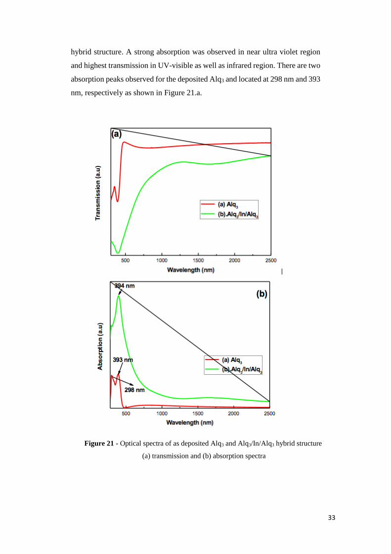
33
hybrid structure. A strong absorption was observed in near ultra violet region
and highest transmission in UV-visible as well as infrared region. There are two
absorption peaks observed for the deposited Alq3 and located at 298 nm and 393
nm, respectively as shown in Figure 21.a.
Figure 21 - Optical spectra of as deposited Alq3 and Alq3/In/Alq3 hybrid structure
(a) transmission and (b) absorption spectra

34
A single strong absorption was found at 393 nm and red-shift was observed
for Alq3/In/ Alq3 hybrid structure. The strong absorption and red shift is mainly
due to Indium (In) sandwiching in the hybrid structure as seen Figure 21.b.
Figure 22 shows the optical band energy for as deposited Alq3 and hybrid
structure film. The direct band gap value was calculated using standard relation
[64]. The couple of band gap values are found to be 2.87eV and 3.34 eV for as
deposited Alq3 as shown in figure 22.a.
2.0 2.5 3.0 3.5 4.0
(h
)
(a.u
)
Photon Energy (eV)
(a). Alq3
2.87 eV 3.34 eV
1.0 1.5 2.0 2.5 3.0
(h
)
(a.u
)
Photon Energy (eV)
(b). Alq3/In/Alq
3
2.49 eV
Figure 22 - Optical energy band gap (a) Alq3 and (b) Alq3/In/Alq3 hybrid structure

35
The theoretical optical band gap value of value Alq3 is obtained at 2.80 eV
and experiment values is 2.87 eV. The calculated band gap value is a good
agreement with previous reports [63]. In this case, two optical band gaps were
observed, and it owns unique optical properties due to preparation method. A
single band gap was found, and the value is 2.49 eV for hybrid structure as seen
in figure 16.b. The decrease in the optical band gap can be related to mixed
surface morphological in SEM images.
Figure 23 shows the PL spectra of Alq3 and Alq3/In/Alq3 hybrid structure
film. All the films were excited at 400 nm at room temperature. Three emission
bands were observed in the visible region, which is centered at 451, 513 and
638 nm for as deposited Alq3 film as seen figure 23.a.A couple of new emission
bands were observed at 479 and 562 nm for Alq3/In/Alq3 hybrid structure. This
is mainly due to the new composite formation and impact of In layer [23].
Spherical grain with rod shapes and Indium plays important role in the new
emission band in the hybrid structure. This kind of emission properties are much
need to design and fabricate optoelectronic devices.
400 450 500 550 600 650 700 750
PL
em
iss
ion
(a
.u)
Wavelength (nm)
(a). Alq3
(b). Alq3/In/Alq
3
451 nm 479 nm 562 nm
513 nm
638 nm
Figure 23- PL emission spectra (a) Alq3 and (b). Alq3/In/Alq3 hybrid structure

36
3.2.5 Partial Conclusion
The hybrid Alq3/ In/Alq3 composite structure were successfully deposited
over the glass substrate using thermal evaporation technique. The structural,
optical and morphological properties were studied through several analytical
techniques. The XRD pattern reveals that single diffraction peak is found at
31.77° and belongs to Indium (In) in the hybrid sandwich structure and the
calculated grain size is found to be 11 nm for hybrid structure. The hybird
structure shows the mixed surface of spherical grains with rod like shape.
A single band gap was found to be 2.49 eV for hybrid structure. A couple of
new emission bands were observed at 479 and 562 nm for hybrid structure. The
hybrid structure shows unique surface, optical band and emission band
properties. Further studies on the effect of annealing and different metal layers
other than In could result in better understanding of the properties of this
composite material.
3.3 Impact of Annealing on Hybrid Alq3 / In / Alq3
Composite Thin Films
3.3.1 Experimental Details
The hybrid Alq3/ In/Alq3 composite structure were deposited over the glass
substrate using thermal evaporation technique at ambient temperature as shown in
Figure 24. The thicknesses of each layer were controlled, and rate of evaporation
was maintained as 1-3 Å/sec using an in-situ quartz crystal monitor. The hybrid
sandwich structure was taken for annealing process and placed in the substrate heater
setup. The annealing was done under the vacuum in the chamber. The temperatures
were varied in between 150°C and 350°C for about 30 min and the pressure range
was maintained as 10-5 – 10-6m.bar. After that all the films were taken for structural,
optical and morphological studies.

37
Figure 24 -Alq3/In/Alq3 hybrid sandwich structure
3.3.2 Structural Studies
Figure 25 shows the Alq3/In/Alq3 hybrid sandwich structure film annealed at
different temperatures. A single diffraction peak was observed at 32.77˚
corresponding to (1 0 1) for as deposited films as shown figure 19.a. It is
noteworthy to mention that alternate layers of indium and Alq3, leads to form
the Alq3/In/Alq3 composite.
10 20 30 40 50 60 70 80 90
(10
0)
(10
1)
Inte
ns
ity
(a
.u)
2 (deg)
(d). 350oC
(c). 250oC
(b). 150oC
(a). As deposited
Figure 25 - X-ray diffraction pattern of hybrid sandwich structure (a) as deposited,
(b)150°C, (c) 250°C and (d) 350°C
38
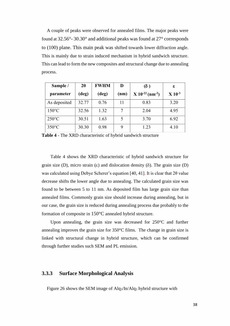
A couple of peaks were observed for annealed films. The major peaks were
found at 32.56°- 30.30° and additional peaks was found at 27° corresponds
to (100) plane. This main peak was shifted towards lower diffraction angle.
This is mainly due to strain induced mechanism in hybrid sandwich structure.
This can lead to form the new composites and structural change due to annealing
process.
Table 4 - The XRD characteristic of hybrid sandwich structure
Table 4 shows the XRD characteristic of hybrid sandwich structure for
grain size (D), micro strain () and dislocation density (). The grain size (D)
was calculated using Debye Scherer’s equation [40, 41]. It is clear that 2θ value
decrease shifts the lower angle due to annealing. The calculated grain size was
found to be between 5 to 11 nm. As deposited film has large grain size than
annealed films. Commonly grain size should increase during annealing, but in
our case, the grain size is reduced during annealing process due probably to the
formation of composite in 150°C annealed hybrid structure.
Upon annealing, the grain size was decreased for 250°C and further
annealing improves the grain size for 350°C films. The change in grain size is
linked with structural change in hybrid structure, which can be confirmed
through further studies such SEM and PL emission.
3.3.3 Surface Morphological Analysis
Figure 26 shows the SEM image of Alq3/In/Alq3 hybrid structure with
Sample /
parameter
2θ
(deg)
FWHM
(deg)
D
(nm)
( )
X 10-22 (nm-2)
X 10-3
As deposited 32.77 0.76 11 0.83 3.20
150°C 32.56 1.32 7 2.04 4.95
250°C 30.51 1.63 5 3.70 6.92
350°C 30.30 0.98 9 1.23 4.10

39
different annealing temperatures. The hybird structure shows the mixed surface
of spherical grains with rod like shape as seen in figure 26.a.
The spherical grains may be Indium (In) atom and rod like a structure
corresponds to Alq3. Upon annealing, the non-uniform surface with random
orientaion of smaller grains was observed for at 150°C as shown in figure 26.b.
Figure 26 -SEM image of Alq3/In/ Alq3 hybrid structure with different annealing
temperatures
Upon further annealing, the spherical grains was spread over the surface for
250°C films as displayed in figure 26.c.Where as mixed spherical grains and
nanorod was observed for 350°C films as seen figure 26.d. It is clearlyseen that
the rods were grown over the spherical grains and spherical grains may be
Indium atom. Different kind of morphology was observed for different
annealing temperatures.

40
3.3.4 Optical Studies
Figure 27 shows the optical spectra of Alq3/In/ Alq3 hybrid structure for
different annealing temperature. Strong absorption was observed in near ultra
violet region and highest transmission in infrared region for higher annealing
temperature. The absorption shoulder was observed at around 400 nm for all the
samples.
500 1000 1500 2000 2500
Tra
ns
mis
sio
n (
a.u
)
Wavelength (nm)
(a). Asdeposited
(b). 150oC
(c). 250oC
(d). 350oC
(b)
500 1000 1500 2000 2500
Ab
so
rpti
on
(a
.u)
Wavelength (nm)
(a). Asdeposited
(b). 150oC
(c). 250oC
(d). 350oC
Figure 27 -Optical absorption spectra of of Alq3/In/ Alq3 hybrid structure with different
annealing temperatures
b)
a)

41
The absorption edge was shifted towards higher wavelength region for higher
annealing temperature. Broad absorption was observed in UV-Visible region
for 350°C films.
Figure 28 shows the optical band energy for Alq3/In/ Alq3 hybrid structure
with different annealing temperatures. The calculated direct band gap values are
found to vary between 1.90 to 2.67 eV with the function of annealing
temperature and are lower than the Alq3 films.
Figure 28 -Optical energy band gap of Alq3/In/ Alq3 hybrid structure with
different annealing temperatures

42
The film annealed at 250°C shows a wider band gap than other films due to
uniform spherical grains over the surface. It is also directly linked with quantum
size effect during annealing process. The changes in band gap values reflect
structural changes upon annealing at different temperatures. The increase in
band gap gives information about quantum confinement in hybrid structure. The
blue shift, optical splitting and increase in band gap are evident for templating
confinement effect. Different energy bands are need for optoelectronic device
in particularly LEDs and OLED applications.
Figure 29 shows the PL spectra of Alq3/In/Alq3 hybrid structure for different
annealing temperatures. All the films were excited at 400 nm at room
temperature. A couple of emission was observed in the UV-Visible region. One
emission in blue region (479 nm) and another emission occur in green region
(564 nm). Upon annealing, single emission was observed at 517 nm due to
mixed rod and spherical grains surface. The emission bands were observed at
455 and 593 nm for 250°C as seen in figure 29.c. This is mainly due to the new
composite formation and impact of In layer [60].
450 500 550 600 650 700
PL
em
iss
ion
in
ten
sit
y (
a.u
)
Wavelength (nm)
(a). AD
(b). 150oC
(c). 250oC
(d). 350oC
455 nm 479 nm
517 nm564 nm 593 nm
501 nm
Figure 29 -PL emission spectra of Alq3/In/Alq3 hybrid structure with different
annealing temperatures

43
3.3.4 Partial Conclusion
Post deposition annealing is appreciable in thin films for a better nucleation
process which could result in better morphology. Because that the annealed
Alq3/In/Alq3 hybrid investigation. However in this work, at 150º and 250º the
grain size decreased and at 350º the grain size increase. An investigation is
necessary to understand if that event was due to the insufficient time or the
temperature was inadequate or if there was a structural change.
Structural, optical and morphological properties were studied with the
function of annealing temperatures. XRD pattern reveals the single diffraction
peak of Indium (In) and calculated grain is varied from 5 to11 nm with different
annealing temperatures. The hybird structure shows unique morphology such as
spherical grains and rod like shape. The calculate band gap was found to be 1.90
and 2.67 eV with function of annealing.
The change in band gap values and grains reflects quantum size effect and
quantum confinement properties. The PL emission almost covers UV-Visible
ranges, which can be useful to fabricate OLED devices. The hybrid structure
shows unique surface, optical band and emission band properties.
4 Final Conclusion
Analyzing the results obtained, it can be observed that the metals were not
modified significantly the optical properties of the film, except the Indium. The
morphological analysis shows the different structures and it can be observed
due the variation of the grain size and the energy surface. It clear that the choice
of the metal has a vital importance on morphology of the formed film.
A very large structural and optical changes were observed when the Indium
was added in the sandwich structure. When the PL spectra is analyzed, the
Alq3/In/Alq3 showed a new emission, with another wavelength and because that
great attention to study the impact of Indium layer in the sandwich structure.
A great attention can be given to the annealed Alq3/In/Alq3 sandwich grain
size. Its common the grain size increase with the temperature, but in this case,

44
until the 250º C, the grain size decrease. The appearance of a new plan was
observed. Meanwhile, the morphological studies showed the Alq3 in different
depositions shapes. At 250º, apparently, the Alq3 is not observed in the surface
and at 350º C, the Alq3 is showed in rods form and it were grown over the
spherical grains.
Understanding the properties changes, it possible be able to apply each thin
film analyzed in OLED structures for the purpose of moving forward the
Material Science.
5 Suggestions for Future Studies
A suggestion for future works may be an in-depth analysis of the morphology of
the Alq3/In/Alq3 and understand more why the structure is so different.
A multi-layer analysis is too important to study how the Indium is organized with
more than one layer, and it is interesting study a possible property change.
The discussed topic of this work is in increasing research for the advancement of
materials science, a deepening of this study is relevant.
45
6 Bibliographic References
1. W. Brütting, M. Cölle, C. Gärditz, “The Isomerism of the
Alq3 Molecule: Evidence from Structural, Thermal and Photophysical
Investigations”, Journal of Molecular Structure, v. 36, n. 2, pp. 669-680,
2002.
2. Sumitomo Chemical , “Global Organic Light-emitting Diode (OLED) Materials
Market 2017”, Available in: https://www.openpr.com/news/583660/Global-
Organic-Light-emitting-Diode-OLED-Materials-Market-2017-DuPont-Merck-
Sumitomo-Chemical-Universal-Display.html, accessed in 06 May, 2018.
3. Agency for Science, Technology and Research, “True blue light emission could
make OLED displays the next big thing in consumer electronics”, available in:
https://phys.org/news/2011-06-true-blue-emission-oled-big.html, accessed in:
06 May, 2018
4. Kyushu University, “Fundamental Structure of OLEDs”, available in:
http://www.cstf.kyushu-u.ac.jp, accessed in: 06 May, 2018.
5. Hyper Physics, “Bragg”, available in : http://hyperphysics.phy-astr.gsu.edu
/hbase/quantum/bragg.html, accessed in : 06 May, 2018.
6. Sobarwiki2013, “Schematic of UV-Visible Spectrophotometer”, available in:
https://commons.wikimedia.org/wiki/File:Schematic_of_UV_visible_spectrop
hotometer.html, accessed in 07 May, 2018.
7. Chemical Libre Texts, “Photoluminescence Spectroscopy”, available in:
https://chem.libretexts.org/Textbook_Maps/Analytical_Chemistry/Book%3A_
Analytical_Chemistry_2.0_(Harvey)/10_Spectroscopic_Methods/10.6%3A_P
hotoluminescence_Spectroscopy.html, accessed in: 07 May, 2018.
8. Renishaw plc., “Photoluminescence Spectroscopy”, available in :
http://www.renishaw.de/de/photoluminescence-explained—25809101.html,
accessed in: 07 May, 2018.
9. Education in Chemistry, “Elements Information”, available in:
https://eic.rsc.org/elements/indium/2020012.article.html, accessed in: 07 May,
2018.
10. E. Fred. Schubert, “Light-Emitting Diodes”, 3 ed., New York, Cambridge
University Press, 2018.

46
11. J. Dittmer, R. Lazzaroni, P. Leclere, P. Moretti, M. Granstrom, K. Petritsch, E.
A. Marseglia, R. H. Friend, J. L. Bredas, H. Rost and A. B. Holmes, “Crystal
Network Formation in Organic Solar Cells,” Solar Energy Materials and
Solar Cells, v. 61, pp. 53-61, 2000.
12. M. Cuba, G. Muralidharan, “Effect of Thermal Annealing on the Structural and
Optical Properties of Tris‐(8‐hydroxyquinoline)Aluminum(III) (Alq3) Films”,
Luminescence, v. 30, n. 3, pp. 352-357, 2015.
13. D.J. Williams, “Organic Electroluminescent Diodes”, Photonics Spectra,
2003, pp. 116-120.
14. J. Majer, M. Reade, “Isomerism in the Metal Derivatives of 8-
hydroxyquinoline”, Chemical Communications, v. 1, pp. 58-59, 1970.
15. A. Curioni, W. Andreoni, “Atom-resolved electronic spectra for
Alq₃ from theory and experiment”, Applied Physics Letters, v.72, n.13,
pp.1575-1577, 1998.
16. B. C. Lin, C. P. Cheng, Z. Q. You, C. P. Hsu, “Charge Transport Properties of
Tris(8-hydroxyquinolinato)aluminum(III): Why It Is an Electron Transporter”,
Journal of the American Chemical Society, v. 127, n. 1, pp. 66–67, 2005.
17. L. S. Hung, C. W. Tang, M. G. Mason, “ Enhanced Electron Injection in Organic
Electroluminescence Devices Using an Al/LiF Electrode”, Application
Physics Letters, v.70, pp. 152-154, 1997.
18. M. Cölle, J. Gmeiner, W. Milius, H. Hillebrecht, and W. Brütting, “Preparation
and Characterization of Blue‐Luminescent Tris(8‐hydroxyquinoline)‐
aluminum (Alq3)”, Advanced Functional Materials, v. 13, pp. 108-112, 2003.
19. G. Baldacchini, S. Gagliardi, R.M. Montereali, A. Pace, R.B. Pode, “Optical
Spectroscopy of Tris(8- Hydroxyquinoline)Aluminium Thin Films”,
Phylosophical Magazine, v. 82, n 6, pp. 669-680, 2002.
20. C.W. Tang, S.A. Van Slyke, “Organic Electroluminescent Diodes”,
Application Physics Letters, v. 51, pp. 913-915, 1987.
21. B. R. Kanchibotla, K. Garre, D. Aurongze, “Correlated Growth of Organic
Material Tris (8-hydroxyquinoline) Aluminum (Alq3) and its Relation to
Optical Properties”, Journal of Applied Physics, v. 106, pp. 096101-1 -
096101-3, 2009.

47
22. M.M. Nahass, A. M. Farid, A. A. Atta, “Structural and Optical Properties of
Tris(8-hydroxyquinoline) Aluminum (III) (Alq3) Thermal Evaporated Thin
Films”, Journal of Alloys and Compounds, v. 507, n. 1, pp. 112-119, 2010.
23. R. H. Friend, Gymer, R. W.,A. B. Holmes, J.H. Burroughes, R. N. Marks,
C. Taliani, D. D. C. Bradley, A. Brédas, J. L. Lögdlund, W. R. Salaneck,
“Electroluminescence in Conjugated Polymers”, Nature, v. 397, n. 6715, pp.
121-128, 1999.
24. G. E. Jabbour, B. Kippelen, N. R. Armstrong, N. Peyghambarian, “Aluminum
Based Cathode Structure for Enhanced Electron Injection in Electroluminescent
Organic Devices”, Application Physic Letters, v.73, n.9, pp. 1185-1187, 1998.
25. C. W. Tang, S. A. VanSlyke, “Organic Electroluminescent Diodes” Application
Physics Letters, v. 51, pp. 913-915, 1987.
26. G. Destriau, J. Saddy, “Preparation of Luminescent Substances. Electrical Field
Effect”, Journal Physic Radium, v.6, n.1, pp. 12-16, 1945.
27. Z. Yin, B. Wang, G. Chen, “One-dimensional 8-hydroxyquinoline Metal
Complex Nanomaterials: Synthesis, Optoelectronic Properties,
and Applications”, Journal of Materials Science, v.46, n. 8, pp. 2397-2410,
2011.
28. H. Uoyama, K. Goushi, K. Shizu,H. Nomura, C. Adachi,
“Highly Efficient Organic Light-emitting Diodes from Delayed Fluorescence”,
Nature, v.492, n. 7428, pp.234, 2012.
29. T. A. Hopkins, K. Meerholz, S. Shaheen, M. L. Anderson, A. Schmidt, B.
Kippelen, A. B. Padias, H. K. Hall, N. Peyghambarian, N. R. Armstrong,
“Substituted Aluminum and Zinc Quinolates with Blue-Shifted
Absorbance/Luminescence Bands: Synthesis and Spectroscopic,
Photoluminescence, and Electroluminescence Characterization”, Chemical
Materials, v.8, n.2 pp. 344–351, 1996
30. C. H. Cheung, A. B. Djurišić, C. Y. Kwong, H. L. Tam, K. W. Cheah, Z. T. Liu,
W. K. Chan, A. D. Rakić, “Change of the Emission Spectra in Organic Light
Emitting Diodes by Layer Thickness Modification”, Applied Physics Letters,
v. 5, n.14, pp. 2944-2946, 2004.
31. J. S. Salafsky, “Exciton Dissociation, Charge Transport, and Recombination in
Ultrathin, Conjugated Polymer, TiO2 Nanocrystal Intermixed Composites,”
Physical Review, v. 59, n. 16, pp. 10885-10894, 1999.

48
32. W. U. Huynh, J. J. Dittmer and A. P. Alivisatos, “Hybrid Nanorod, Polymer
Solar Cells”, Science, v. 295, n. 5564, pp. 2425-2427, 2002.
33. J. Dittmer, R. Lazzaroni, P. Leclere, P. Moretti, M. Granstrom, K. Petritsch, E.
A. Marseglia, R. H. Friend, J. L. Bredas, H. Rost and A. B. Holmes, “Crystal
Network Formation in Organic Solar Cells,” Solar Energy Materials and
Solar Cells, v. 61, pp. 53-61, 2000.
34. V. M. Burlakov, K. Kawata, H. E. Assender, G. A. D. Briggs, A. Ruseckas and
I. D. W. Samuel, “Discrete Hopping Model of Exciton Transport in Disordered
Media,” Physical Review, v. 72, n. 7, 2005.
35. S. A. Choulis, M. K. Mathai and V.-E. Choong, “Influence of Metallic
Nanoparticles on the Performance of Organic Electrophosphorescence
Devices,” Applied Physics Letters, v. 88, n 21, 2006.
36. S. A. Carter, J. C. Scott and J. Brock, “Enhanced Luminance in Polymer
Composite Light Emitting Diodes,” Applied Physics Letters, v. 71, n. 9, pp.
1145-1147, 1997.
37. A. Petrella, M. Tamborra, P. D. Cozzoli, M. L. Curri, M. Striccoli, P. Cosma,
G. M. Farinola, F. Babudri, F. Naso and A. Agostiano, “TiO2 Nanocrystals—
MEH-PPV Composite Thin Films as Photoactive Material,” Thin Solid Films,
v. 451-452, pp. 64-68, 2014.
38. A. A. Madhavan, G. G. Kumar, S. Kalluri, J. Joseph, S. Nagarajan, S. Nair, K.
R. V. Subramanian and A. Balakrishnan, “Effect of Embedded Plasmonic Au
Nanoparticles on Photocatalysis of Electro Spun TiO2 Nanofibers,” Journal of
Nanoscience and Nanotechnology, v. 12, n. 10, pp. 7963-7967, 2012.
39. R. Schlaf, H. Murata and Z. H. Kafafi, “Work Function Measurements on
Indium Tin Oxide Films,” Journal of Electron Spectroscopy and Related
Phenomena, v. 120, n. 1-3, pp. 149-154, 2011.
40. K. Kompoliti, “Copper”, Journal of the Neurological Sciences, v. 357, pp.478-
478, 2015.
41. L. M. Dennis, J. A. Bridgman, “Gallium”, Journal of the American Chemical
Society, v. 40, n. 10 pp.1531-1561, 1918.
42. K. Haris, A. Kramida, A. Tauheed, “Extended and Revised Analysis of Singly
Ionized Tin: Sn”, PhysicaScripta, v. 89, n.11 pp.115403-115424, 2014.
43. S. E. Harrison, B. Zhou, Y. Huo, A. Pushp, A. J. Kellock, S. S. P. Parkin, J. S.
Harris,Y. Chen, T. Hesjedal, “Preparation of Layered Thin Film Samples for
49
Angle-Resolved Photoemission Spectroscopy”, Applied Physics Letters, v.
105, n. 12, 2014.
44. A. Petrella, M. Tamborra, P. D. Cozzoli, M. L. Curri, M. Striccoli, P. Cosma,
G. M. Farinola, F. Babudri, F. Naso and A. Agostiano, “TiO2 Nanocrystals—
MEH-PPV Composite Thin Films as Photoactive Material,” Thin Solid Films,
v. 451-452, pp. 64-68, 2004.
45. A. Moarrefzadeh, “Simulation and Modeling of Physical Vapor Deposition
(PVD)”, WSEAS Transactions on Applied and Theoretical Mechanics, v.7,
v.2, pp. 106-111, 2012.
46. D. M. Mattox, “Physical vapor deposition (PVD)”, Metal Finishing, v. 100, n.
1, pp. 394-408, 2002
47. Donald M. Mattox, “Handbook of Physical Vapor Deposition (PVD) Process”,
2 ed., William Andrew, 2010.
48. D. Dorset, “X-ray Diffraction: A Practical Approach”, Microscopy and
Microanalysis, v. 4, n. 5, pp. 513-515, 1998.
49. B. D. Cullity, “Elements of X-Ray Diffraction,” 2nd Edition, Addison-Wesley
Publishing Company, Boston, 1978.
50. B.E. Warren, “X-Ray Diffraction”, 1 ed., Dover Publications, New York, 1990.
51. T. Mahalingan “Electrosynthesis and characterization of lead oxide thin films”,
Materials Characterization, v.58, pp. 8-9, 2007.
52. D. JunLee, E. YooYoon, , B. HoPark, Hyo WookPark, L JuPark, YuriEstrin, H.
SeopKim, “Dislocation Density-based Finite Element Analysis of Large Strain
Deformation Behavior of Copper Under High-Pressure Torsion”, Acta
Materialia, v.76, pp. 281-293.
53. Y. Zhao, J. Zhang, “Microstrain and grain-size analysis from diffraction peak
width and graphical derivation of highpressure thermomechanics”, Journal of
Applied Crystallography, v. 41, pp. 1095-1108, 2008.
54. N. J. Unakar, J. Y. Tsui, C. V. Harding, “Scanning Electron Microscopy”,
Ophthalmic, v. 13, pp.20-35, 1981.
55. H. H. Perkampus, “UV-Visible Spectroscopy and Its Applications”, 1 ed.
Springer-Verlag, Berlin, 1992.
56. C.Ghosh, B.P.Varma, “Some Optical properties of Amorphous and Crystalline
Antimony Trisulphide Thin Films”, Solid State Communications, v. 31, n. 9,
pp. 683-686, 1979.

50
57. J. Tauc, “Optical Properties of Solids”, Physics Review, v.25, pp. 749, 1970.
58. T. T. Chung-Thuy, L. H. Chi and N. N. Dinh, “Study of Photoluminescent and
Electrical Properties of Nanostructured MEH-PPV/TiO2 Hybrid Films,”
Journal of the Korean Physical Society, v. 54, 2009, pp. 291-295.
59. Challa S.S.R. Kumar , “UV-VIS and Photoluminescence Spectroscopy for
Nanomaterials Characterization”, 1 ed., Springer, New York, 2013.
60. GUO Yao, WANG Zhi-Bing, CUI Yi-Ping, ZHANG Jia-Yu, YE Yong-Hong,
“Tris (8-Hydroxyquinoline) Aluminum Nanostructure Film and Its
Fluorescence Properties”, Chinese Physic Letters, v. 25, pp. 4428, 2008.
61. S. A. Carter, J. C. Scott and J. Brock, “Enhanced Luminance in Polymer
Composite Light Emitting Diodes,” Applied Physics Letters, v. 71, n. 9, pp.
1145-1147, 1997.
62. A. Petrella, M. Tamborra, P. D. Cozzoli, M. L. Curri, M. Striccoli, P. Cosma,
G. M. Farinola, F. Babudri, F. Naso and A. Agostiano, “TiO2 Nanocrystals—
MEH-PPV Composite Thin Films as Photoactive Material,” Thin Solid Films,
v. 451-452, pp. 64-68, 2004.
63. R. L. Zhigang, “Organic Light-Emitting Materials and Devices”, 2 ed., CRC
Press, 2015.
64. M. Duvenhage, M.Ntwaeaborwa, H. G. Visser, P. J. Swarts, J. C. Swarts,
“Determination of the Optical Band Gap of Alq3 and its Derivatives for the Use
in Two-Layer OLEDs, Optical Materials”, v. 42, pp. 193-198, 2015.