Embed Size (px)
Citation preview

© 2008 Microchip Technology Inc. DS39760D
PIC18F2450/4450Data Sheet
24/40/44-Pin High-Performance,12 MIPS, Enhanced Flash,
USB Microcontrollerswith nanoWatt Technology
Note the following details of the code protection feature on Microchip devices:� Microchip products meet the specification contained in their particular Microchip Data Sheet.
� Microchip believes that its family of products is one of the most secure families of its kind on the market today, when used in the intended manner and under normal conditions.
� There are dishonest and possibly illegal methods used to breach the code protection feature. All of these methods, to our knowledge, require using the Microchip products in a manner outside the operating specifications contained in Microchip�s Data Sheets. Most likely, the person doing so is engaged in theft of intellectual property.
� Microchip is willing to work with the customer who is concerned about the integrity of their code.
� Neither Microchip nor any other semiconductor manufacturer can guarantee the security of their code. Code protection does not mean that we are guaranteeing the product as �unbreakable.�
Code protection is constantly evolving. We at Microchip are committed to continuously improving the code protection features of ourproducts. Attempts to break Microchip�s code protection feature may be a violation of the Digital Millennium Copyright Act. If such actsallow unauthorized access to your software or other copyrighted work, you may have a right to sue for relief under that Act.
Information contained in this publication regarding deviceapplications and the like is provided only for your convenienceand may be superseded by updates. It is your responsibility toensure that your application meets with your specifications.MICROCHIP MAKES NO REPRESENTATIONS ORWARRANTIES OF ANY KIND WHETHER EXPRESS ORIMPLIED, WRITTEN OR ORAL, STATUTORY OROTHERWISE, RELATED TO THE INFORMATION,INCLUDING BUT NOT LIMITED TO ITS CONDITION,QUALITY, PERFORMANCE, MERCHANTABILITY ORFITNESS FOR PURPOSE. Microchip disclaims all liabilityarising from this information and its use. Use of Microchipdevices in life support and/or safety applications is entirely atthe buyer�s risk, and the buyer agrees to defend, indemnify andhold harmless Microchip from any and all damages, claims,suits, or expenses resulting from such use. No licenses areconveyed, implicitly or otherwise, under any Microchipintellectual property rights.
DS39760D-page ii
Trademarks
The Microchip name and logo, the Microchip logo, Accuron, dsPIC, KEELOQ, KEELOQ logo, MPLAB, PIC, PICmicro, PICSTART, PRO MATE, rfPIC and SmartShunt are registered trademarks of Microchip Technology Incorporated in the U.S.A. and other countries.
FilterLab, Linear Active Thermistor, MXDEV, MXLAB, SEEVAL, SmartSensor and The Embedded Control Solutions Company are registered trademarks of Microchip Technology Incorporated in the U.S.A.
Analog-for-the-Digital Age, Application Maestro, CodeGuard, dsPICDEM, dsPICDEM.net, dsPICworks, dsSPEAK, ECAN, ECONOMONITOR, FanSense, In-Circuit Serial Programming, ICSP, ICEPIC, Mindi, MiWi, MPASM, MPLAB Certified logo, MPLIB, MPLINK, mTouch, PICkit, PICDEM, PICDEM.net, PICtail, PIC32 logo, PowerCal, PowerInfo, PowerMate, PowerTool, REAL ICE, rfLAB, Select Mode, Total Endurance, UNI/O, WiperLock and ZENA are trademarks of Microchip Technology Incorporated in the U.S.A. and other countries.
SQTP is a service mark of Microchip Technology Incorporated in the U.S.A.
All other trademarks mentioned herein are property of their respective companies.
© 2008, Microchip Technology Incorporated, Printed in the U.S.A., All Rights Reserved.
Printed on recycled paper.
© 2008 Microchip Technology Inc.
Microchip received ISO/TS-16949:2002 certification for its worldwide headquarters, design and wafer fabrication facilities in Chandler and Tempe, Arizona; Gresham, Oregon and design centers in California and India. The Company�s quality system processes and procedures are for its PIC® MCUs and dsPIC® DSCs, KEELOQ® code hopping devices, Serial EEPROMs, microperipherals, nonvolatile memory and analog products. In addition, Microchip�s quality system for the design and manufacture of development systems is ISO 9001:2000 certified.

© 2008 Microchip Technology Inc. DS39760D-page 1
Universal Serial Bus Features:� USB V2.0 Compliant� Low Speed (1.5 Mb/s) and Full Speed (12 Mb/s)� Supports Control, Interrupt, Isochronous and
Bulk Transfers� Supports Up to 32 Endpoints (16 bidirectional)� 256-Byte Dual Access RAM for USB� On-Chip USB Transceiver with On-Chip Voltage
Regulator� Interface for Off-Chip USB Transceiver
Power-Managed Modes:� Run: CPU on, Peripherals on� Idle: CPU off, Peripherals on� Sleep: CPU off, Peripherals off� Idle mode Currents Down to 5.8 μA Typical� Sleep mode Currents Down to 0.1 μA Typical� Timer1 Oscillator: 1.8 μA Typical, 32 kHz, 2V� Watchdog Timer: 2.1 μA Typical� Two-Speed Oscillator Start-up
Flexible Oscillator Structure:� Four Crystal modes, including High-Precision PLL
for USB� Two External Clock modes, up to 48 MHz� Internal 31 kHz Oscillator� Secondary Oscillator using Timer1 @ 32 kHz� Dual Oscillator Options allow Microcontroller and
USB module to Run at Different Clock Speeds� Fail-Safe Clock Monitor:
- Allows for safe shutdown if any clock stops
Peripheral Highlights:� High-Current Sink/Source: 25 mA/25 mA� Three External Interrupts� Three Timer modules (Timer0 to Timer2)� Capture/Compare/PWM (CCP) module:
- Capture is 16-bit, max. resolution 5.2 ns- Compare is 16-bit, max. resolution 83.3 ns- PWM output: PWM resolution is 1 to 10-bit
� Enhanced USART module:- LIN bus support
� 10-Bit, Up to 13-Channel Analog-to-Digital Converter module (A/D): - Up to 100 ksps sampling rate- Programmable acquisition time
Special Microcontroller Features:� C Compiler Optimized Architecture with Optional
Extended Instruction Set� Flash Memory Retention: > 40 Years� Self-Programmable under Software Control� Priority Levels for Interrupts� 8 x 8 Single-Cycle Hardware Multiplier� Extended Watchdog Timer (WDT):
- Programmable period from 4 ms to 131s� Programmable Code Protection� Single-Supply In-Circuit Serial Programming�
(ICSP�) via Two Pins� In-Circuit Debug (ICD) via Two Pins� Optional Dedicated ICD/ICSP Port
(44-pin TQFP devices only)� Wide Operating Voltage Range (2.0V to 5.5V)
Device
Program Memory Data Memory SRAM(bytes)
I/O 10-Bit A/D(ch) CCP EUSART Timers
8/16-BitFlash(bytes)
# Single-Word Instructions
PIC18F2450 16K 8192 768* 23 10 1 1 1/2PIC18F4450 16K 8192 768* 34 13 1 1 1/2
* Includes 256 bytes of dual access RAM used by USB module and shared with data memory.
28/40/44-Pin High-Performance, 12 MIPS, Enhanced Flash, USB Microcontrollers with nanoWatt Technology
PIC18F2450/4450

PIC18F2450/4450
DS39760D-page 2 © 2008 Microchip Technology Inc.
Pin Diagrams
28-Pin QFN
1011
23456
1
87
9
121314 15
1617181920
232425262728
2221
MCLR/VPP/RE3RA0/AN0RA1/AN1
RA2/AN2/VREF-RA3/AN3/VREF+RA4/T0CKI/RCV
RA5/AN4/HLVDINVSS
OSC1/CLKIOSC2/CLKO/RA6
RC0/T1OSO/T1CKIRC1/T1OSI/UOE
RC2/CCP1VUSB
RB7/KBI3/PGDRB6/KBI2/PGCRB5/KBI1/PGMRB4/AN11/KBI0RB3/AN9/VPORB2/AN8/INT2/VMORB1/AN10/INT1RB0/AN12/INT0VDD
VSS
RC7/RX/DTRC6/TX/CKRC5/D+/VPRC4/D-/VM
28-Pin SPDIP, SOIC
PIC
18F2
450
10 11
23
6
1
18192021
22
12 13 1415
87
1617
232425262728
9
PIC18F2450
RC
0/T1
OS
O/T
1CK
I
54
RB
7/K
BI3
/PG
DR
B6/
KB
I2/P
GC
RB
5/K
BI1
/PG
MR
B4/
AN
11/K
BI0
RB3/AN9/VPORB2/AN8/INT2/VMORB1/AN10/INT1RB0/AN12/INT0VDDVSSRC7/RX/DT
RC
6/TX
/CK
RC
5/D
+/V
PR
C4/
D-/V
M
MC
LR/V
PP/R
E3
RA
0/A
N0
RA
1/A
N1
RA2/AN2/VREF-RA3/AN3/VREF+RA4/T0CKI/RCV
RA5/AN4/HLVDINVSS
OSC1/CLKIOSC2/CLKO/RA6
RC
1/T1
OS
I/UO
ER
C2/
CC
P1
VU
SB

PIC18F2450/4450
© 2008 Microchip Technology Inc. DS39760D-page 3
Pin Diagrams (Continued)
44-Pin QFN
1011
23
6
1
18 19 20 21 2212 13 14 15
38
87
44 43 42 41 40 3916 17
2930313233
232425262728
36 3435
9
37
RA
3/A
N3/
VRE
F+R
A2/A
N2/
VRE
F-R
A1/
AN
1R
A0/
AN
0M
CLR
/VP
P/R
E3R
B7/
KB
I3/P
GD
RB
6/K
BI2
/PG
CR
B5/
KBI1
/PG
MNC
RC
6/TX
/CK
RC
5/D
+/V
PR
C4/
D-/V
MR
D3
RD
2R
D1
RD
0VU
SB
RC
2/C
CP
1R
C1/
T1O
SI/U
OE
RC
0/T1
OSO
/T1C
KI
OSC2/CLKO/RA6OSC1/CLKIVSS
AVDD
RA5/AN4/HLVDINRA4/T0CKI/RCV
RC7/RX/DTRD4RD5RD6
VSS
VDDRB0/AN12/INT0RB1/AN10/INT1
RB2/AN8/INT2/VMO
RB
3/A
N9/
VPO
RD7 54 AVSS
VDD
AVDD
PIC18F4450
RB4
/AN
11/K
BI0
RE0/AN5RE1/AN6RE2/AN7
40-Pin PDIP
RB7/KBI3/PGDRB6/KBI2/PGCRB5/KBI1/PGMRB4/AN11/KBI0RB3/AN9/VPORB2/AN8/INT2/VMORB1/AN10/INT1RB0/AN12/INT0VDDVSS
RD7RD6RD5RD4RC7/RX/DTRC6/TX/CKRC5/D+/VPRC4/D-/VMRD3RD2
MCLR/VPP/RE3RA0/AN0RA1/AN1
RA2/AN2/VREF-RA3/AN3/VREF+RA4/T0CKI/RCV
RA5/AN4/HLVDINRE0/AN5RE1/AN6RE2/AN7
VDDVSS
OSC1/CLKIOSC2/CLKO/RA6
RC0/T1OSO/T1CKIRC1/T1OSI/UOE
RC2/CCP1VUSBRD0RD1
1234567891011121314151617181920
4039383736353433323130292827262524232221
PIC
18F4
450

PIC18F2450/4450
DS39760D-page 4 © 2008 Microchip Technology Inc.
Pin Diagrams (Continued)
1011
23
6
1
18 19 20 21 2212 13 14 15
38
87
44 43 42 41 40 3916 17
2930313233
232425262728
36 3435
9
37
RA
3/A
N3/
VRE
F+
RA
1/A
N1
MC
LR/V
PP/R
E3
RC
6/TX
/CK
RC0/T1OSO/T1CKIOSC2/CLKO/RA6OSC1/CLKIVSSVDD
RA5/AN4/HLVDINRA4/T0CKI/RCV
VSSVDD
44-Pin TQFP
54
PIC18F4450
RC7/RX/DTRD4RD5RD6RD7
RB0/AN12/INT0RB1/AN10/INT1
RB2/AN8/INT2/VMORB3/AN9/VPO
RC
1/T1
OS
I/UO
ER
C2/
CC
P1
V US
BR
D0
RD
1R
D2
RD
3R
C4/
D-/V
MR
C5/
D+/
VP
RB
5/KB
I1/P
GM
RB6
/KB
I2/P
GC
RB7
/KB
I3/P
GD
RA
0/A
N0
RA
2/A
N2/
VRE
F-
Note 1: Special ICPORT features are available in select circumstances. For more information, seeSection 18.9 �Special ICPORT Features (Designated Packages Only)�.
RB
4/A
N11
/KB
I0
RE0/AN5RE1/AN6RE2/AN7
NC
/ICC
K(1
) /IC
PG
C(1
)
NC
/ICD
T(1) /IC
PG
D(1
)
NC/ICRST(1)/ICVPP(1)
NC
/ICPO
RTS
(1)
PIC18F2450/4450
© 2008 Microchip Technology Inc. DS39760D-page 5
Table of Contents1.0 Device Overview .......................................................................................................................................................................... 72.0 Oscillator Configurations ............................................................................................................................................................ 233.0 Power-Managed Modes ............................................................................................................................................................. 334.0 Reset .......................................................................................................................................................................................... 415.0 Memory Organization ................................................................................................................................................................. 536.0 Flash Program Memory.............................................................................................................................................................. 737.0 8 x 8 Hardware Multiplier............................................................................................................................................................ 838.0 Interrupts .................................................................................................................................................................................... 859.0 I/O Ports ..................................................................................................................................................................................... 9910.0 Timer0 Module ......................................................................................................................................................................... 11111.0 Timer1 Module ......................................................................................................................................................................... 11512.0 Timer2 Module ......................................................................................................................................................................... 12113.0 Capture/Compare/PWM (CCP) Module ................................................................................................................................... 12314.0 Universal Serial Bus (USB) ...................................................................................................................................................... 12915.0 Enhanced Universal Synchronous Receiver Transmitter (EUSART)....................................................................................... 15316.0 10-Bit Analog-to-Digital Converter (A/D) Module ..................................................................................................................... 17517.0 High/Low-Voltage Detect (HLVD)............................................................................................................................................. 18518.0 Special Features of the CPU.................................................................................................................................................... 19119.0 Instruction Set Summary .......................................................................................................................................................... 21320.0 Development Support............................................................................................................................................................... 26321.0 Electrical Characteristics .......................................................................................................................................................... 26722.0 Packaging Information.............................................................................................................................................................. 295Appendix A: Revision History............................................................................................................................................................. 307Appendix B: Device Differences ........................................................................................................................................................ 308Appendix C: Conversion Considerations ........................................................................................................................................... 309Appendix D: Migration From Baseline to Enhanced Devices ............................................................................................................ 309Appendix E: Migration From Mid-Range to Enhanced Devices ......................................................................................................... 310Appendix F: Migration From High-End to Enhanced Devices............................................................................................................ 310Index ................................................................................................................................................................................................. 311The Microchip Web Site ..................................................................................................................................................................... 319Customer Change Notification Service .............................................................................................................................................. 319Customer Support .............................................................................................................................................................................. 319Reader Response .............................................................................................................................................................................. 320Product Identification System ............................................................................................................................................................ 321
PIC18F2450/4450
DS39760D-page 6 © 2008 Microchip Technology Inc.
TO OUR VALUED CUSTOMERSIt is our intention to provide our valued customers with the best documentation possible to ensure successful use of your Microchipproducts. To this end, we will continue to improve our publications to better suit your needs. Our publications will be refined andenhanced as new volumes and updates are introduced. If you have any questions or comments regarding this publication, please contact the Marketing Communications Department viaE-mail at [email protected] or fax the Reader Response Form in the back of this data sheet to (480) 792-4150. Wewelcome your feedback.
Most Current Data SheetTo obtain the most up-to-date version of this data sheet, please register at our Worldwide Web site at:
http://www.microchip.comYou can determine the version of a data sheet by examining its literature number found on the bottom outside corner of any page.The last character of the literature number is the version number, (e.g., DS30000A is version A of document DS30000).
ErrataAn errata sheet, describing minor operational differences from the data sheet and recommended workarounds, may exist for currentdevices. As device/documentation issues become known to us, we will publish an errata sheet. The errata will specify the revisionof silicon and revision of document to which it applies.To determine if an errata sheet exists for a particular device, please check with one of the following:� Microchip�s Worldwide Web site; http://www.microchip.com� Your local Microchip sales office (see last page)When contacting a sales office, please specify which device, revision of silicon and data sheet (include literature number) you areusing.
Customer Notification SystemRegister on our web site at www.microchip.com to receive the most current information on all of our products.
PIC18F2450/4450
© 2008 Microchip Technology Inc. DS39760D-page 7
1.0 DEVICE OVERVIEWThis document contains device-specific information forthe following devices:
This family of devices offers the advantages of allPIC18 microcontrollers � namely, high computationalperformance at an economical price � with the addi-tion of high-endurance, Enhanced Flash programmemory. In addition to these features, thePIC18F2450/4450 family introduces design enhance-ments that make these microcontrollers a logicalchoice for many high-performance, power sensitiveapplications.
1.1 New Core Features
1.1.1 nanoWatt TECHNOLOGYAll of the devices in the PIC18F2450/4450 familyincorporate a range of features that can significantlyreduce power consumption during operation. Keyitems include:
� Alternate Run Modes: By clocking the controller from the Timer1 source or the internal RC oscillator, power consumption during code execution can be reduced by as much as 90%.
� Multiple Idle Modes: The controller can also run with its CPU core disabled but the peripherals still active. In these states, power consumption can be reduced even further, to as little as 4% of normal operation requirements.
� On-the-Fly Mode Switching: The power-managed modes are invoked by user code during operation, allowing the user to incorporate power-saving ideas into their application�s software design.
� Low Consumption in Key Modules: The power requirements for both Timer1 and the Watchdog Timer are minimized. See Section 21.0 �Electrical Characteristics� for values.
1.1.2 UNIVERSAL SERIAL BUS (USB)Devices in the PIC18F2450/4450 family incorporate afully featured Universal Serial Bus communicationsmodule that is compliant with the USB SpecificationRevision 2.0. The module supports both low-speed andfull-speed communication for all supported datatransfer types. It also incorporates its own on-chiptransceiver and 3.3V regulator and supports the use ofexternal transceivers and voltage regulators.
1.1.3 MULTIPLE OSCILLATOR OPTIONS AND FEATURES
All of the devices in the PIC18F2450/4450 family offertwelve different oscillator options, allowing users a widerange of choices in developing application hardware.These include:
� Four Crystal modes using crystals or ceramic resonators.
� Four External Clock modes, offering the option of using two pins (oscillator input and a divide-by-4 clock output) or one pin (oscillator input, with the second pin reassigned as general I/O).
� An INTRC source (approximately 31 kHz, stable over temperature and VDD). This option frees an oscillator pin for use as an additional general purpose I/O.
� A Phase Lock Loop (PLL) frequency multiplier, available to both the High-Speed Crystal and External Oscillator modes, which allows a wide range of clock speeds from 4 MHz to 48 MHz.
� Asynchronous dual clock operation, allowing the USB module to run from a high-frequency oscillator while the rest of the microcontroller is clocked from an internal low-power oscillator.
The internal oscillator provides a stable referencesource that gives the family additional features forrobust operation:
� Fail-Safe Clock Monitor: This option constantly monitors the main clock source against a reference signal provided by the internal oscillator. If a clock failure occurs, the controller is switched to the internal oscillator, allowing for continued low-speed operation or a safe application shutdown.
� Two-Speed Start-up: This option allows the internal oscillator to serve as the clock source from Power-on Reset, or wake-up from Sleep mode, until the primary clock source is available.
� PIC18F2450 � PIC18F4450

PIC18F2450/4450
DS39760D-page 8 © 2008 Microchip Technology Inc.
1.2 Other Special Features� Memory Endurance: The Enhanced Flash cells
for program memory are rated to last for many thousands of erase/write cycles � up to 100,000.
� Self-Programmability: These devices can write to their own program memory spaces under internal software control. By using a bootloader routine, located in the protected Boot Block at the top of program memory, it becomes possible to create an application that can update itself in the field.
� Extended Instruction Set: The PIC18F2450/4450 family introduces an optional extension to the PIC18 instruction set, which adds 8 new instructions and an Indexed Literal Offset Addressing mode. This extension, enabled as a device configuration option, has been specifically designed to optimize re-entrant application code originally developed in high-level languages such as C.
� Enhanced Addressable USART: This serial communication module is capable of standard RS-232 operation and provides support for the LIN bus protocol. Other enhancements include Automatic Baud Rate Detection and a 16-bit Baud Rate Generator for improved resolution.
� 10-Bit A/D Converter: This module incorporates programmable acquisition time, allowing for a channel to be selected and a conversion to be initiated, without waiting for a sampling period and thus, reducing code overhead.
� Dedicated ICD/ICSP Port: These devices introduce the use of debugger and programming pins that are not multiplexed with other micro-controller features. Offered as an option in select packages, this feature allows users to develop I/O intensive applications while retaining the ability to program and debug in the circuit.
1.3 Details on Individual Family Members
Devices in the PIC18F2450/4450 family are availablein 28-pin and 40/44-pin packages. Block diagrams forthe two groups are shown in Figure 1-1 and Figure 1-2.
The devices are differentiated from each other in thefollowing two ways:
1. A/D channels (10 for 28-pin devices, 13 for 40/44-pin devices).
2. I/O ports (3 bidirectional ports and 1 input onlyport on 28-pin devices, 5 bidirectional ports on40/44-pin devices).
All other features for devices in this family are identical.These are summarized in Table 1-1.
The pinouts for all devices are listed in Table 1-2 andTable 1-3.
Like all Microchip PIC18 devices, members of thePIC18F2450/4450 family are available as both standardand low-voltage devices. Standard devices withEnhanced Flash memory, designated with an �F� in thepart number (such as PIC18F2450), accommodate anoperating VDD range of 4.2V to 5.5V. Low-voltage parts,designated by �LF� (such as PIC18LF2450), functionover an extended VDD range of 2.0V to 5.5V.
PIC18F2450/4450
© 2008 Microchip Technology Inc. DS39760D-page 9
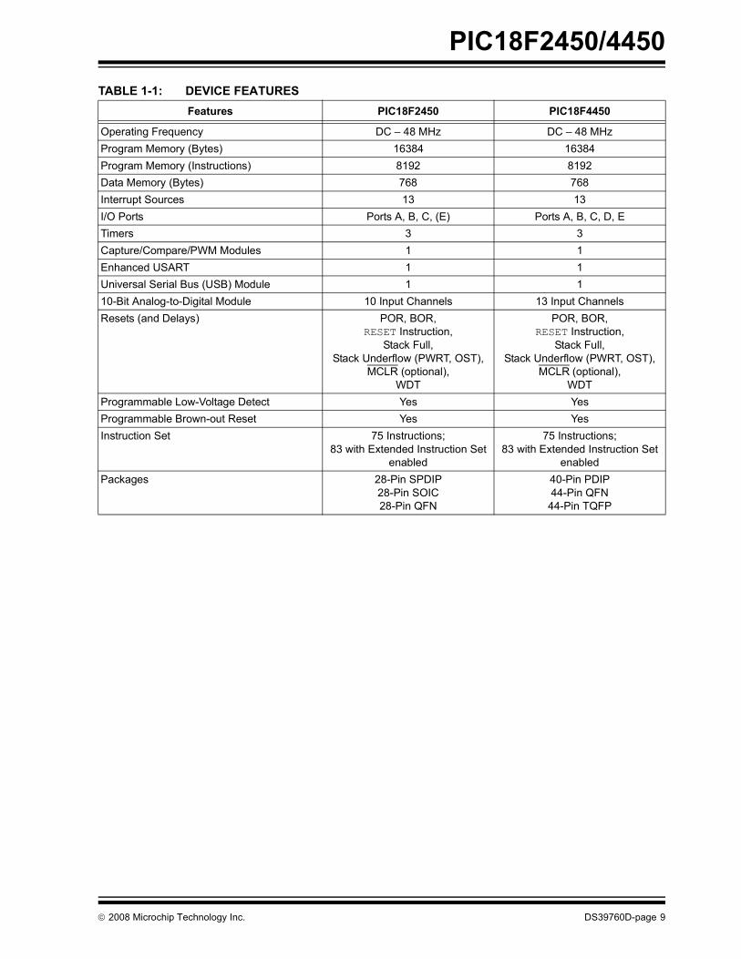
TABLE 1-1: DEVICE FEATURES Features PIC18F2450 PIC18F4450
Operating Frequency DC � 48 MHz DC � 48 MHzProgram Memory (Bytes) 16384 16384Program Memory (Instructions) 8192 8192Data Memory (Bytes) 768 768Interrupt Sources 13 13I/O Ports Ports A, B, C, (E) Ports A, B, C, D, ETimers 3 3Capture/Compare/PWM Modules 1 1Enhanced USART 1 1Universal Serial Bus (USB) Module 1 110-Bit Analog-to-Digital Module 10 Input Channels 13 Input ChannelsResets (and Delays) POR, BOR,
RESET Instruction, Stack Full,
Stack Underflow (PWRT, OST), MCLR (optional),
WDT
POR, BOR, RESET Instruction,
Stack Full, Stack Underflow (PWRT, OST),
MCLR (optional),WDT
Programmable Low-Voltage Detect Yes YesProgrammable Brown-out Reset Yes YesInstruction Set 75 Instructions;
83 with Extended Instruction Set enabled
75 Instructions; 83 with Extended Instruction Set
enabledPackages 28-Pin SPDIP
28-Pin SOIC28-Pin QFN
40-Pin PDIP44-Pin QFN
44-Pin TQFP

PIC18F2450/4450
DS39760D-page 10 © 2008 Microchip Technology Inc.
FIGURE 1-1: PIC18F2450 (28-PIN) BLOCK DIAGRAM
Data Latch
Data Memory(2 Kbytes)
Address Latch
Data Address<12>12
AccessBSR4 4
PCH PCL
PCLATH
8
31 Level Stack
Program Counter
PRODLPRODH
8 x 8 Multiply
8
88
ALU<8>
Address Latch
Program Memory(24/32 Kbytes)
Data Latch
20
8
8
Table Pointer<21>
inc/dec logic
21
8
Data Bus<8>
Table Latch8
IR
12
3
ROM Latch
PCLATU
PCU
PORTE
MCLR/VPP/RE3(1)
Note 1: RE3 is multiplexed with MCLR and is only available when the MCLR Resets are disabled.2: OSC1/CLKI and OSC2/CLKO are only available in select oscillator modes and when these pins are not being used as digital I/O. Refer
to Section 2.0 �Oscillator Configurations� for additional information.
W
Instruction Bus <16>
STKPTR Bank
8
8
8
BITOP
FSR0FSR1FSR2
inc/dec
Address
12
Decode
logic
EUSART
Timer2Timer1Timer0
USB
InstructionDecode &
Control
State MachineControl Signals
Power-upTimer
OscillatorStart-up Timer
Power-onReset
WatchdogTimer
OSC1(2)
OSC2(2)
VDD,
Brown-outReset
InternalOscillator
Fail-SafeClock Monitor
ReferenceBand Gap
VSS
MCLR(1)
Block
INTRCOscillator
Single-SupplyProgramming
In-CircuitDebugger
T1OSI
T1OSO
USB VoltageRegulatorVUSB
PORTB
PORTC
RB0/AN12/INT0
RC0/T1OSO/T1CKIRC1/T1OSI/UOERC2/CCP1RC4/D-/VMRC5/D+/VPRC6/TX/CKRC7/RX/DT
RB1/AN10/INT1RB2/AN8/INT2/VMORB3/AN9/VPORB4/AN11/KBI0RB5/KBI1/PGMRB6/KBI2/PGCRB7/KBI3/PGD
PORTA
RA4/T0CKI/RCVRA5/AN4/HLVDIN
RA3/AN3/VREF+RA2/AN2/VREF-RA1/AN1RA0/AN0
OSC2/CLKO/RA6
CCP1
ADC10-Bit
BORHLVD

PIC18F2450/4450
© 2008 Microchip Technology Inc. DS39760D-page 11
FIGURE 1-2: PIC18F4450 (40/44-PIN) BLOCK DIAGRAM
InstructionDecode &
Control
Data Latch
Data Memory(2 Kbytes)
Address Latch
Data Address<12>12
AccessBSR4 4
PCH PCL
PCLATH
8
31 Level Stack
Program Counter
PRODLPRODH
8 x 8 Multiply
8
BITOP88
ALU<8>
Address Latch
Program Memory(24/32 Kbytes)
Data Latch
20
8
8
Table Pointer<21>
inc/dec logic
21
8
Data Bus<8>
Table Latch8
IR
12
3
ROM Latch
PORTD
PCLATU
PCU
PORTE
MCLR/VPP/RE3(1)RE2/AN7
RE0/AN5RE1/AN6
Note 1: RE3 is multiplexed with MCLR and is only available when the MCLR Resets are disabled.2: OSC1/CLKI and OSC2/CLKO are only available in select oscillator modes and when these pins are not being used as digital I/O. Refer
to Section 2.0 �Oscillator Configurations� for additional information.3: These pins are only available on 44-pin TQFP under certain conditions. Refer to Section 18.9 �Special ICPORT Features (Designated
Packages Only)� for additional information.
EUSART 10-Bit ADC
Timer2Timer1Timer0
CCP1
W
Instruction Bus <16>
STKPTR Bank
8
State MachineControl Signals
8
8
Power-upTimer
OscillatorStart-up Timer
Power-onReset
WatchdogTimer
OSC1(2)
OSC2(2)
VDD,
Brown-outReset
InternalOscillator
Fail-SafeClock Monitor
ReferenceBand Gap
VSS
MCLR(1)
Block
INTRCOscillator
Single-SupplyProgramming
In-CircuitDebugger
T1OSI
T1OSO
PORTA
PORTB
PORTC
RA4/T0CKI/RCVRA5/AN4/HLVDIN
RB0/AN12/INT0
RC0/T1OSO/T1CKIRC1/T1OSI/UOERC2/CCP1RC4/D-/VMRC5/D+/VPRC6/TX/CKRC7/RX/DT
RA3/AN3/VREF+RA2/AN2/VREF-RA1/AN1RA0/AN0
RB1/AN10/INT1RB2/AN8/INT2/VMORB3/AN9/VPO
OSC2/CLKO/RA6
RB4/AN11/KBI0RB5/KBI1/PGMRB6/KBI2/PGCRB7/KBI3/PGD
USB
FSR0FSR1FSR2
inc/dec
Address
12
Decode
logic
USB VoltageRegulator
VUSB
ICRST(3)
ICPGC(3)
ICPGD(3)
ICPORTS(3)
RD0RD1RD2RD3RD4RD5RD6RD7
BORHLVD
PIC18F2450/4450
DS39760D-page 12 © 2008 Microchip Technology Inc.
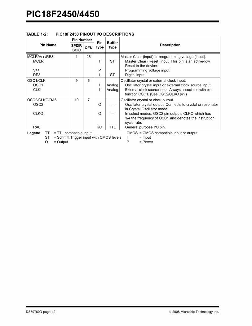
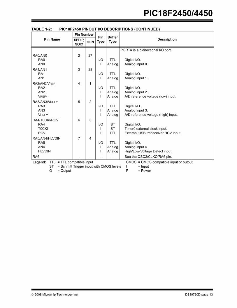
TABLE 1-2: PIC18F2450 PINOUT I/O DESCRIPTIONS
Pin NamePin Number
PinType
BufferType DescriptionSPDIP,
SOIC QFN
MCLR/VPP/RE3MCLR
VPPRE3
1 26I
PI
ST
ST
Master Clear (input) or programming voltage (input).Master Clear (Reset) input. This pin is an active-low Reset to the device.Programming voltage input.Digital input.
OSC1/CLKIOSC1CLKI
9 6II
AnalogAnalog
Oscillator crystal or external clock input.Oscillator crystal input or external clock source input. External clock source input. Always associated with pin function OSC1. (See OSC2/CLKO pin.)
OSC2/CLKO/RA6OSC2
CLKO
RA6
10 7O
O
I/O
�
�
TTL
Oscillator crystal or clock output.Oscillator crystal output. Connects to crystal or resonatorin Crystal Oscillator mode.In select modes, OSC2 pin outputs CLKO which has1/4 the frequency of OSC1 and denotes the instruction cycle rate. General purpose I/O pin.
Legend: TTL = TTL compatible input CMOS = CMOS compatible input or output ST = Schmitt Trigger input with CMOS levels I = Input O = Output P = Power
PIC18F2450/4450
© 2008 Microchip Technology Inc. DS39760D-page 13
PORTA is a bidirectional I/O port.RA0/AN0
RA0AN0
2 27I/OI
TTLAnalog
Digital I/O.Analog input 0.
RA1/AN1RA1AN1
3 28I/OI
TTLAnalog
Digital I/O.Analog input 1.
RA2/AN2/VREF-RA2AN2VREF-
4 1I/OII
TTLAnalogAnalog
Digital I/O.Analog input 2.A/D reference voltage (low) input.
RA3/AN3/VREF+RA3AN3VREF+
5 2I/OII
TTLAnalogAnalog
Digital I/O.Analog input 3.A/D reference voltage (high) input.
RA4/T0CKI/RCVRA4T0CKIRCV
6 3I/OII
STSTTTL
Digital I/O.Timer0 external clock input.External USB transceiver RCV input.
RA5/AN4/HLVDINRA5AN4HLVDIN
7 4I/OII
TTLAnalogAnalog
Digital I/O.Analog input 4.High/Low-Voltage Detect input.
RA6 � � � � See the OSC2/CLKO/RA6 pin.
TABLE 1-2: PIC18F2450 PINOUT I/O DESCRIPTIONS (CONTINUED)
Pin NamePin Number
PinType
BufferType DescriptionSPDIP,
SOIC QFN
Legend: TTL = TTL compatible input CMOS = CMOS compatible input or output ST = Schmitt Trigger input with CMOS levels I = Input O = Output P = Power

PIC18F2450/4450
DS39760D-page 14 © 2008 Microchip Technology Inc.
PORTB is a bidirectional I/O port. PORTB can be software programmed for internal weak pull-ups on all inputs.
RB0/AN12/INT0RB0AN12INT0
21 18I/OII
TTLAnalog
ST
Digital I/O.Analog input 12. External interrupt 0.
RB1/AN10/INT1RB1AN10INT1
22 19I/OII
TTLAnalog
ST
Digital I/O.Analog input 10. External interrupt 1.
RB2/AN8/INT2/VMORB2AN8INT2VMO
23 20I/OIIO
TTLAnalog
ST�
Digital I/O.Analog input 8.External interrupt 2.External USB transceiver VMO output.
RB3/AN9/VPORB3AN9VPO
24 21I/OIO
TTLAnalog
�
Digital I/O.Analog input 9.External USB transceiver VPO output.
RB4/AN11/KBI0RB4AN11KBI0
25 22I/OII
TTLAnalog
TTL
Digital I/O.Analog input 11.Interrupt-on-change pin.
RB5/KBI1/PGMRB5KBI1PGM
26 23I/OI
I/O
TTLTTLST
Digital I/O.Interrupt-on-change pin.Low-Voltage ICSP� Programming enable pin.
RB6/KBI2/PGCRB6KBI2PGC
27 24I/OI
I/O
TTLTTLST
Digital I/O.Interrupt-on-change pin. In-Circuit Debugger and ICSP programming clock pin.
RB7/KBI3/PGDRB7KBI3PGD
28 25I/OI
I/O
TTLTTLST
Digital I/O.Interrupt-on-change pin. In-Circuit Debugger and ICSP programming data pin.
TABLE 1-2: PIC18F2450 PINOUT I/O DESCRIPTIONS (CONTINUED)
Pin NamePin Number
PinType
BufferType DescriptionSPDIP,
SOIC QFN
Legend: TTL = TTL compatible input CMOS = CMOS compatible input or output ST = Schmitt Trigger input with CMOS levels I = Input O = Output P = Power
PIC18F2450/4450
© 2008 Microchip Technology Inc. DS39760D-page 15
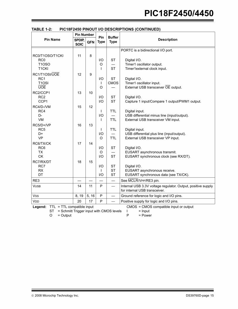
PORTC is a bidirectional I/O port.RC0/T1OSO/T1CKI
RC0T1OSOT1CKI
11 8I/OOI
ST�ST
Digital I/O.Timer1 oscillator output. Timer1external clock input.
RC1/T1OSI/UOERC1T1OSIUOE
12 9I/OIO
STCMOS
�
Digital I/O.Timer1 oscillator input.External USB transceiver OE output.
RC2/CCP1RC2CCP1
13 10I/OI/O
STST
Digital I/O.Capture 1 input/Compare 1 output/PWM1 output.
RC4/D-/VMRC4D-VM
15 12I
I/OI
TTL�
TTL
Digital input.USB differential minus line (input/output).External USB transceiver VM input.
RC5/D+/VPRC5D+VP
16 13I
I/OO
TTL�
TTL
Digital input.USB differential plus line (input/output).External USB transceiver VP input.
RC6/TX/CKRC6TXCK
17 14I/OO
I/O
ST�ST
Digital I/O.EUSART asynchronous transmit. EUSART synchronous clock (see RX/DT).
RC7/RX/DTRC7RXDT
18 15I/OI
I/O
STSTST
Digital I/O.EUSART asynchronous receive.EUSART synchronous data (see TX/CK).
RE3 � � � � See MCLR/VPP/RE3 pin.VUSB 14 11 P � Internal USB 3.3V voltage regulator. Output, positive supply
for internal USB transceiver.VSS 8, 19 5, 16 P � Ground reference for logic and I/O pins.VDD 20 17 P � Positive supply for logic and I/O pins.
TABLE 1-2: PIC18F2450 PINOUT I/O DESCRIPTIONS (CONTINUED)
Pin NamePin Number
PinType
BufferType DescriptionSPDIP,
SOIC QFN
Legend: TTL = TTL compatible input CMOS = CMOS compatible input or output ST = Schmitt Trigger input with CMOS levels I = Input O = Output P = Power

PIC18F2450/4450
DS39760D-page 16 © 2008 Microchip Technology Inc.
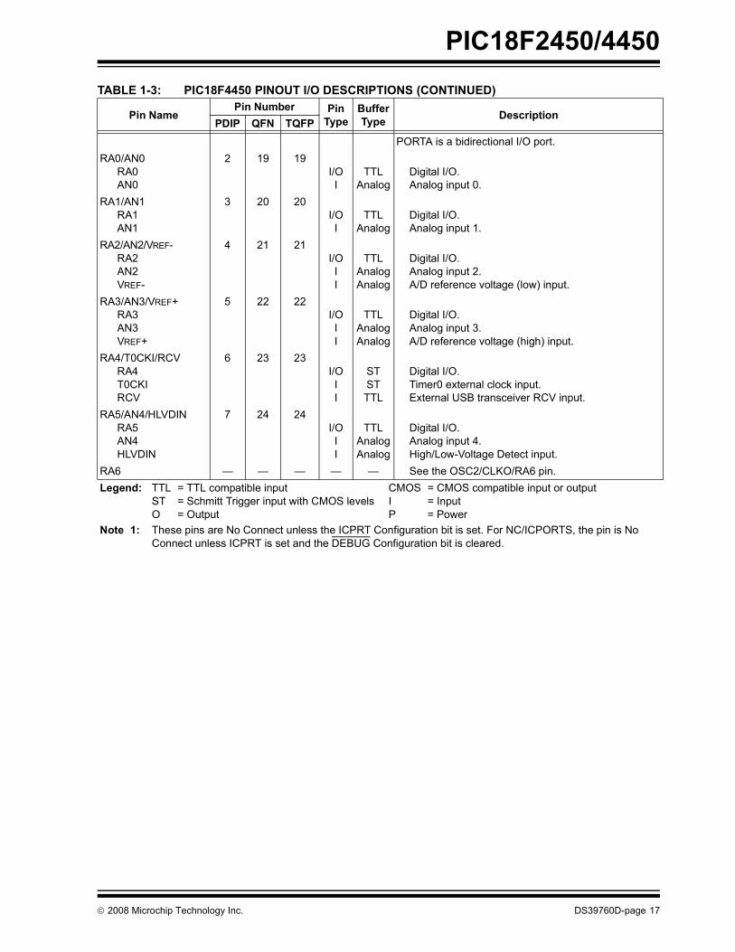
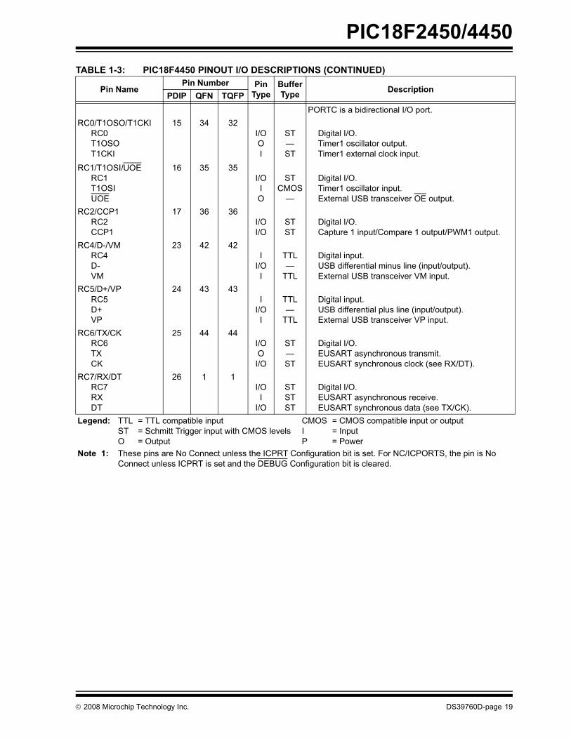
TABLE 1-3: PIC18F4450 PINOUT I/O DESCRIPTIONS
Pin NamePin Number Pin
TypeBufferType Description
PDIP QFN TQFP
MCLR/VPP/RE3MCLR
VPPRE3
1 18 18I
PI
ST
�ST
Master Clear (input) or programming voltage (input).Master Clear (Reset) input. This pin is an active-low Reset to the device.Programming voltage input.Digital input.
OSC1/CLKIOSC1CLKI
13 32 30II
AnalogAnalog
Oscillator crystal or external clock input.Oscillator crystal input or external clock source input. External clock source input. Always associated with pin function OSC1. (See OSC2/CLKO pin.)
OSC2/CLKO/RA6OSC2
CLKO
RA6
14 33 31O
O
I/O
�
�
TTL
Oscillator crystal or clock output.Oscillator crystal output. Connects to crystal or resonator in Crystal Oscillator mode.In select modes, OSC2 pin outputs CLKO which has1/4 the frequency of OSC1 and denotes the instruction cycle rate. General purpose I/O pin.
Legend: TTL = TTL compatible input CMOS = CMOS compatible input or output ST = Schmitt Trigger input with CMOS levels I = Input O = Output P = Power
Note 1: These pins are No Connect unless the ICPRT Configuration bit is set. For NC/ICPORTS, the pin is No Connect unless ICPRT is set and the DEBUG Configuration bit is cleared.
PIC18F2450/4450
© 2008 Microchip Technology Inc. DS39760D-page 17
PORTA is a bidirectional I/O port.RA0/AN0
RA0AN0
2 19 19I/OI
TTLAnalog
Digital I/O.Analog input 0.
RA1/AN1RA1AN1
3 20 20I/OI
TTLAnalog
Digital I/O.Analog input 1.
RA2/AN2/VREF-RA2AN2VREF-
4 21 21I/OII
TTLAnalogAnalog
Digital I/O.Analog input 2.A/D reference voltage (low) input.
RA3/AN3/VREF+RA3AN3VREF+
5 22 22I/OII
TTLAnalogAnalog
Digital I/O.Analog input 3.A/D reference voltage (high) input.
RA4/T0CKI/RCVRA4T0CKIRCV
6 23 23I/OII
STSTTTL
Digital I/O.Timer0 external clock input.External USB transceiver RCV input.
RA5/AN4/HLVDINRA5AN4HLVDIN
7 24 24I/OII
TTLAnalogAnalog
Digital I/O.Analog input 4.High/Low-Voltage Detect input.
RA6 � � � � � See the OSC2/CLKO/RA6 pin.
TABLE 1-3: PIC18F4450 PINOUT I/O DESCRIPTIONS (CONTINUED)
Pin NamePin Number Pin
TypeBufferType Description
PDIP QFN TQFP
Legend: TTL = TTL compatible input CMOS = CMOS compatible input or output ST = Schmitt Trigger input with CMOS levels I = Input O = Output P = Power
Note 1: These pins are No Connect unless the ICPRT Configuration bit is set. For NC/ICPORTS, the pin is No Connect unless ICPRT is set and the DEBUG Configuration bit is cleared.
PIC18F2450/4450
DS39760D-page 18 © 2008 Microchip Technology Inc.
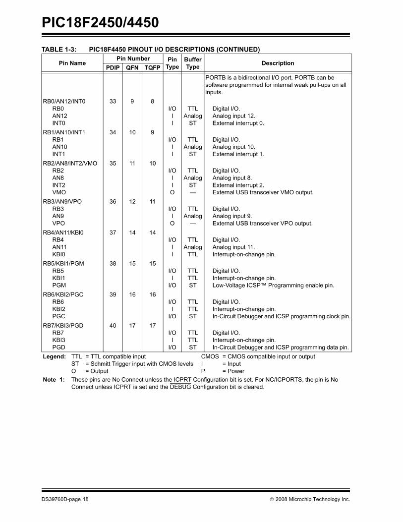
PORTB is a bidirectional I/O port. PORTB can be software programmed for internal weak pull-ups on all inputs.
RB0/AN12/INT0RB0AN12INT0
33 9 8I/OII
TTLAnalog
ST
Digital I/O.Analog input 12. External interrupt 0.
RB1/AN10/INT1RB1AN10INT1
34 10 9I/OII
TTLAnalog
ST
Digital I/O.Analog input 10. External interrupt 1.
RB2/AN8/INT2/VMORB2AN8INT2VMO
35 11 10I/OIIO
TTLAnalog
ST�
Digital I/O.Analog input 8.External interrupt 2.External USB transceiver VMO output.
RB3/AN9/VPORB3AN9VPO
36 12 11I/OIO
TTLAnalog
�
Digital I/O.Analog input 9.External USB transceiver VPO output.
RB4/AN11/KBI0RB4AN11KBI0
37 14 14I/OII
TTLAnalog
TTL
Digital I/O.Analog input 11.Interrupt-on-change pin.
RB5/KBI1/PGMRB5KBI1PGM
38 15 15I/OI
I/O
TTLTTLST
Digital I/O.Interrupt-on-change pin.Low-Voltage ICSP� Programming enable pin.
RB6/KBI2/PGCRB6KBI2PGC
39 16 16I/OI
I/O
TTLTTLST
Digital I/O.Interrupt-on-change pin. In-Circuit Debugger and ICSP programming clock pin.
RB7/KBI3/PGDRB7KBI3PGD
40 17 17I/OI
I/O
TTLTTLST
Digital I/O.Interrupt-on-change pin. In-Circuit Debugger and ICSP programming data pin.
TABLE 1-3: PIC18F4450 PINOUT I/O DESCRIPTIONS (CONTINUED)
Pin NamePin Number Pin
TypeBufferType Description
PDIP QFN TQFP
Legend: TTL = TTL compatible input CMOS = CMOS compatible input or output ST = Schmitt Trigger input with CMOS levels I = Input O = Output P = Power
Note 1: These pins are No Connect unless the ICPRT Configuration bit is set. For NC/ICPORTS, the pin is No Connect unless ICPRT is set and the DEBUG Configuration bit is cleared.
PIC18F2450/4450
© 2008 Microchip Technology Inc. DS39760D-page 19
PORTC is a bidirectional I/O port.RC0/T1OSO/T1CKI
RC0T1OSOT1CKI
15 34 32I/OOI
ST�ST
Digital I/O.Timer1 oscillator output. Timer1 external clock input.
RC1/T1OSI/UOERC1T1OSIUOE
16 35 35I/OIO
STCMOS
�
Digital I/O.Timer1 oscillator input.External USB transceiver OE output.
RC2/CCP1RC2CCP1
17 36 36I/OI/O
STST
Digital I/O.Capture 1 input/Compare 1 output/PWM1 output.
RC4/D-/VMRC4D-VM
23 42 42I
I/OI
TTL�
TTL
Digital input.USB differential minus line (input/output).External USB transceiver VM input.
RC5/D+/VPRC5D+VP
24 43 43I
I/OI
TTL�
TTL
Digital input.USB differential plus line (input/output).External USB transceiver VP input.
RC6/TX/CKRC6TXCK
25 44 44I/OO
I/O
ST�ST
Digital I/O.EUSART asynchronous transmit. EUSART synchronous clock (see RX/DT).
RC7/RX/DTRC7RXDT
26 1 1I/OI
I/O
STSTST
Digital I/O.EUSART asynchronous receive.EUSART synchronous data (see TX/CK).
TABLE 1-3: PIC18F4450 PINOUT I/O DESCRIPTIONS (CONTINUED)
Pin NamePin Number Pin
TypeBufferType Description
PDIP QFN TQFP
Legend: TTL = TTL compatible input CMOS = CMOS compatible input or output ST = Schmitt Trigger input with CMOS levels I = Input O = Output P = Power
Note 1: These pins are No Connect unless the ICPRT Configuration bit is set. For NC/ICPORTS, the pin is No Connect unless ICPRT is set and the DEBUG Configuration bit is cleared.
PIC18F2450/4450
DS39760D-page 20 © 2008 Microchip Technology Inc.
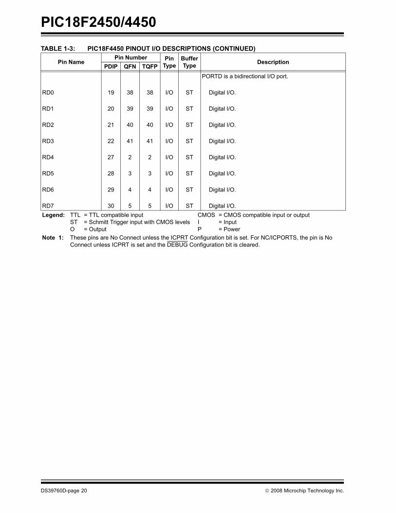
PORTD is a bidirectional I/O port.
RD0 19 38 38 I/O ST Digital I/O.
RD1 20 39 39 I/O ST Digital I/O.
RD2 21 40 40 I/O ST Digital I/O.
RD3 22 41 41 I/O ST Digital I/O.
RD4 27 2 2 I/O ST Digital I/O.
RD5 28 3 3 I/O ST Digital I/O.
RD6 29 4 4 I/O ST Digital I/O.
RD7 30 5 5 I/O ST Digital I/O.
TABLE 1-3: PIC18F4450 PINOUT I/O DESCRIPTIONS (CONTINUED)
Pin NamePin Number Pin
TypeBufferType Description
PDIP QFN TQFP
Legend: TTL = TTL compatible input CMOS = CMOS compatible input or output ST = Schmitt Trigger input with CMOS levels I = Input O = Output P = Power
Note 1: These pins are No Connect unless the ICPRT Configuration bit is set. For NC/ICPORTS, the pin is No Connect unless ICPRT is set and the DEBUG Configuration bit is cleared.
PIC18F2450/4450
© 2008 Microchip Technology Inc. DS39760D-page 21
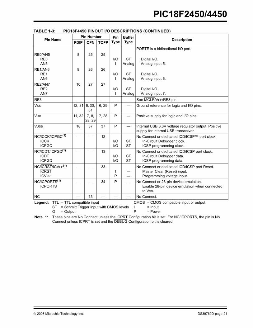
PORTE is a bidirectional I/O port.RE0/AN5
RE0AN5
8 25 25I/OI
STAnalog
Digital I/O.Analog input 5.
RE1/AN6RE1AN6
9 26 26I/OI
STAnalog
Digital I/O.Analog input 6.
RE2/AN7RE2AN7
10 27 27I/OI
STAnalog
Digital I/O.Analog input 7.
RE3 � � � � � See MCLR/VPP/RE3 pin.VSS 12, 31 6, 30,
316, 29 P � Ground reference for logic and I/O pins.
VDD 11, 32 7, 8, 28, 29
7, 28 P � Positive supply for logic and I/O pins.
VUSB 18 37 37 P � Internal USB 3.3V voltage regulator output. Positive supply for internal USB transceiver.
NC/ICCK/ICPGC(1)
ICCKICPGC
� � 12I/OI/O
STST
No Connect or dedicated ICD/ICSP� port clock.In-Circuit Debugger clock. ICSP programming clock.
NC/ICDT/ICPGD(1)
ICDTICPGD
� � 13I/OI/O
STST
No Connect or dedicated ICD/ICSP port clock.In-Circuit Debugger data.ICSP programming data.
NC/ICRST/ICVPP(1)
ICRSTICVPP
� � 33IP
��
No Connect or dedicated ICD/ICSP port Reset.Master Clear (Reset) input.Programming voltage input.
NC/ICPORTS(1)
ICPORTS� � 34 P � No Connect or 28-pin device emulation.
Enable 28-pin device emulation when connectedto VSS.
NC � 13 � � � No Connect.
TABLE 1-3: PIC18F4450 PINOUT I/O DESCRIPTIONS (CONTINUED)
Pin NamePin Number Pin
TypeBufferType Description
PDIP QFN TQFP
Legend: TTL = TTL compatible input CMOS = CMOS compatible input or output ST = Schmitt Trigger input with CMOS levels I = Input O = Output P = Power
Note 1: These pins are No Connect unless the ICPRT Configuration bit is set. For NC/ICPORTS, the pin is No Connect unless ICPRT is set and the DEBUG Configuration bit is cleared.

PIC18F2450/4450
DS39760D-page 22 © 2008 Microchip Technology Inc.
NOTES:
PIC18F2450/4450
© 2008 Microchip Technology Inc. DS39760D-page 23
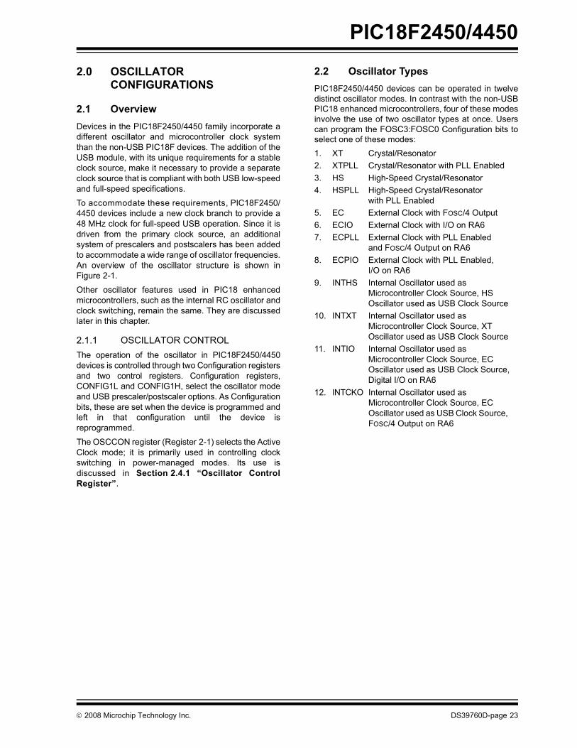
2.0 OSCILLATOR CONFIGURATIONS
2.1 OverviewDevices in the PIC18F2450/4450 family incorporate adifferent oscillator and microcontroller clock systemthan the non-USB PIC18F devices. The addition of theUSB module, with its unique requirements for a stableclock source, make it necessary to provide a separateclock source that is compliant with both USB low-speedand full-speed specifications.
To accommodate these requirements, PIC18F2450/4450 devices include a new clock branch to provide a48 MHz clock for full-speed USB operation. Since it isdriven from the primary clock source, an additionalsystem of prescalers and postscalers has been addedto accommodate a wide range of oscillator frequencies.An overview of the oscillator structure is shown inFigure 2-1.
Other oscillator features used in PIC18 enhancedmicrocontrollers, such as the internal RC oscillator andclock switching, remain the same. They are discussedlater in this chapter.
2.1.1 OSCILLATOR CONTROLThe operation of the oscillator in PIC18F2450/4450devices is controlled through two Configuration registersand two control registers. Configuration registers,CONFIG1L and CONFIG1H, select the oscillator modeand USB prescaler/postscaler options. As Configurationbits, these are set when the device is programmed andleft in that configuration until the device isreprogrammed.
The OSCCON register (Register 2-1) selects the ActiveClock mode; it is primarily used in controlling clockswitching in power-managed modes. Its use isdiscussed in Section 2.4.1 �Oscillator ControlRegister�.
2.2 Oscillator TypesPIC18F2450/4450 devices can be operated in twelvedistinct oscillator modes. In contrast with the non-USBPIC18 enhanced microcontrollers, four of these modesinvolve the use of two oscillator types at once. Userscan program the FOSC3:FOSC0 Configuration bits toselect one of these modes:1. XT Crystal/Resonator2. XTPLL Crystal/Resonator with PLL Enabled3. HS High-Speed Crystal/Resonator4. HSPLL High-Speed Crystal/Resonator
with PLL Enabled5. EC External Clock with FOSC/4 Output6. ECIO External Clock with I/O on RA67. ECPLL External Clock with PLL Enabled
and FOSC/4 Output on RA68. ECPIO External Clock with PLL Enabled,
I/O on RA69. INTHS Internal Oscillator used as
Microcontroller Clock Source, HS Oscillator used as USB Clock Source
10. INTXT Internal Oscillator used asMicrocontroller Clock Source, XT Oscillator used as USB Clock Source
11. INTIO Internal Oscillator used as Microcontroller Clock Source, ECOscillator used as USB Clock Source,Digital I/O on RA6
12. INTCKO Internal Oscillator used as Microcontroller Clock Source, EC Oscillator used as USB Clock Source, FOSC/4 Output on RA6

PIC18F2450/4450
DS39760D-page 24 © 2008 Microchip Technology Inc.
2.2.1 OSCILLATOR MODES AND USB OPERATION
Because of the unique requirements of the USBmodule, a different approach to clock operation isnecessary. In previous PIC® microcontrollers, all coreand peripheral clocks were driven by a single oscillatorsource; the usual sources were primary, secondary orthe internal oscillator. With PIC18F2450/4450 devices,the primary oscillator becomes part of the USB moduleand cannot be associated to any other clock source.Thus, the USB module must be clocked from theprimary clock source; however, the microcontrollercore and other peripherals can be separately clockedfrom the secondary or internal oscillators as before.
Because of the timing requirements imposed by USB,an internal clock of either 6 MHz or 48 MHz is requiredwhile the USB module is enabled. Fortunately, themicrocontroller and other peripherals are not requiredto run at this clock speed when using the primaryoscillator. There are numerous options to achieve theUSB module clock requirement and still provide flexi-bility for clocking the rest of the device from the primaryoscillator source. These are detailed in Section 2.3�Oscillator Settings for USB�.
FIGURE 2-1: PIC18F2450/4450 CLOCK DIAGRAM
PIC18F2450/4450
FOSC3:FOSC0
Secondary Oscillator
T1OSCENEnableOscillator
T1OSO
T1OSI
Clock Source Option for Other Modules
OSC1
OSC2
Sleep
Primary Oscillator
XT, HS, EC, ECIO
T1OSC
CPU
Peripherals
IDLEN
MU
X
OSCCON<6:4>
WDT, PWRT, FSCM
Internal Oscillator
ClockControl
OSCCON<1:0>
and Two-Speed Start-up
96 MHzPLL
PLLDIV<2:0>
CPUDIV<1:0>
01
0
1÷ 2
PLL
Pre
scal
er
MU
X
111
110
101
100
011
010
001
000÷ 1
÷ 2
÷ 3
÷ 4
÷ 5
÷ 6
÷ 10÷ 12
11
10
01
00PLL
Pos
tsca
ler
÷ 2
÷ 3
÷ 4
÷ 6
USB
USBDIV
FOSC3:FOSC0
HSPLL, ECPLL,
11
10
01
00
Osc
illato
r Pos
tsca
ler
÷ 1
÷ 2
÷ 3
÷ 4
CPUDIV<1:0>
1
0
Peripheral
FSEN
÷ 4
USB Clock Source
XTPLL, ECPIO
PrimaryClock
(4 MHz Input Only)
Internal RC Oscillator31.25 kHz

PIC18F2450/4450
© 2008 Microchip Technology Inc. DS39760D-page 25
2.2.2 CRYSTAL OSCILLATOR/CERAMIC RESONATORS
In HS, HSPLL, XT and XTPLL Oscillator modes, acrystal or ceramic resonator is connected to the OSC1and OSC2 pins to establish oscillation. Figure 2-2shows the pin connections.
The oscillator design requires the use of a parallel cutcrystal.
FIGURE 2-2: CRYSTAL/CERAMIC RESONATOR OPERATION (XT, HS OR HSPLL CONFIGURATION)
TABLE 2-1: CAPACITOR SELECTION FOR CERAMIC RESONATORS
TABLE 2-2: CAPACITOR SELECTION FOR CRYSTAL OSCILLATOR
An internal postscaler allows users to select a clockfrequency other than that of the crystal or resonator.Frequency division is determined by the CPUDIVConfiguration bits. Users may select a clock frequencyof the oscillator frequency, or 1/2, 1/3 or 1/4 of thefrequency.
An external clock may also be used when the micro-controller is in HS Oscillator mode. In this case, theOSC2/CLKO pin is left open (Figure 2-3).
Note: Use of a series cut crystal may give a fre-quency out of the crystal manufacturer�sspecifications.
Typical Capacitor Values Used:
Mode Freq OSC1 OSC2
XT 4.0 MHz 33 pF 33 pFHS 8.0 MHz
16.0 MHz27 pF22 pF
27 pF22 pF
Capacitor values are for design guidance only. These capacitors were tested with the resonatorslisted below for basic start-up and operation. Thesevalues are not optimized.
Different capacitor values may be required to produceacceptable oscillator operation. The user should testthe performance of the oscillator over the expectedVDD and temperature range for the application.
See the notes following Table 2-2 for additionalinformation.
Resonators Used:
4.0 MHz8.0 MHz
16.0 MHz
Note 1: See Table 2-1 and Table 2-2 for initial values of C1 and C2.
2: A series resistor (RS) may be required for AT strip cut crystals.
3: RF varies with the oscillator mode chosen.
C1(1)
C2(1)
XTAL
OSC2
OSC1
RF(3)
Sleep
To
Logic
PIC18FXXXXRS(2)
Internal
Osc Type Crystal Freq
Typical Capacitor Values Tested:
C1 C2
XT 4 MHz 27 pF 27 pFHS 4 MHz 27 pF 27 pF
8 MHz 22 pF 22 pF20 MHz 15 pF 15 pF
Capacitor values are for design guidance only. These capacitors were tested with the crystals listedbelow for basic start-up and operation. These valuesare not optimized.Different capacitor values may be required to produceacceptable oscillator operation. The user should testthe performance of the oscillator over the expectedVDD and temperature range for the application.
See the notes following this table for additionalinformation.
Crystals Used:
4 MHz8 MHz20 MHz
Note 1: Higher capacitance increases the stabilityof oscillator but also increases the start-uptime.
2: When operating below 3V VDD, or whenusing certain ceramic resonators at anyvoltage, it may be necessary to use theHS mode or switch to a crystal oscillator.
3: Since each resonator/crystal has its owncharacteristics, the user should consultthe resonator/crystal manufacturer forappropriate values of externalcomponents.
4: Rs may be required to avoid overdrivingcrystals with low drive level specification.
5: Always verify oscillator performance overthe VDD and temperature range that isexpected for the application.

PIC18F2450/4450
DS39760D-page 26 © 2008 Microchip Technology Inc.
FIGURE 2-3: EXTERNAL CLOCK INPUT OPERATION (HS OSC CONFIGURATION)
2.2.3 EXTERNAL CLOCK INPUTThe EC, ECIO, ECPLL and ECPIO Oscillator modesrequire an external clock source to be connected to theOSC1 pin. There is no oscillator start-up time requiredafter a Power-on Reset or after an exit from Sleepmode.
In the EC and ECPLL Oscillator modes, the oscillatorfrequency divided by 4 is available on the OSC2 pin.This signal may be used for test purposes or tosynchronize other logic. Figure 2-4 shows the pinconnections for the EC Oscillator mode.
FIGURE 2-4: EXTERNAL CLOCKINPUT OPERATION(EC AND ECPLL CONFIGURATION)
The ECIO and ECPIO Oscillator modes function like theEC and ECPLL modes, except that the OSC2 pinbecomes an additional general purpose I/O pin. The I/Opin becomes bit 6 of PORTA (RA6). Figure 2-5 showsthe pin connections for the ECIO Oscillator mode.
FIGURE 2-5: EXTERNAL CLOCK INPUT OPERATION (ECIO AND ECPIO CONFIGURATION)
The internal postscaler for reducing clock frequency inXT and HS modes is also available in EC and ECIOmodes.
2.2.4 PLL FREQUENCY MULTIPLIERPIC18F2450/4450 devices include a Phase LockedLoop (PLL) circuit. This is provided specifically for USBapplications with lower speed oscillators and can alsobe used as a microcontroller clock source.
The PLL is enabled in HSPLL, XTPLL, ECPLL andECPIO Oscillator modes. It is designed to produce afixed 96 MHz reference clock from a fixed 4 MHz input.The output can then be divided and used for both theUSB and the microcontroller core clock. Because thePLL has a fixed frequency input and output, there areeight prescaling options to match the oscillator inputfrequency to the PLL.
There is also a separate postscaler option for derivingthe microcontroller clock from the PLL. This allows theUSB peripheral and microcontroller to use the sameoscillator input and still operate at different clockspeeds. In contrast to the postscaler for XT, HS and ECmodes, the available options are 1/2, 1/3, 1/4 and 1/6of the PLL output.
The HSPLL, ECPLL and ECPIO modes make use ofthe HS mode oscillator for frequencies up to 48 MHz.The prescaler divides the oscillator input by up to 12 toproduce the 4 MHz drive for the PLL. The XTPLL modecan only use an input frequency of 4 MHz which drivesthe PLL directly.
FIGURE 2-6: PLL BLOCK DIAGRAM (HS MODE)
OSC1
OSC2Open
Clock fromExt. System PIC18FXXXX
(HS Mode)
OSC1/CLKI
OSC2/CLKOFOSC/4
Clock fromExt. System PIC18FXXXX
OSC1/CLKI
I/O (OSC2)RA6
Clock fromExt. System PIC18FXXXX
MU
X
VCO
LoopFilter
andPrescaler
OSC2
OSC1
PLL Enable
FIN
FOUT
SYSCLK
PhaseComparator
HS/EC/ECIO/XT Oscillator Enable
÷24
(from CONFIG1H Register)
Oscillator
PIC18F2450/4450
© 2008 Microchip Technology Inc. DS39760D-page 27
2.2.5 INTERNAL OSCILLATORThe PIC18F2450/4450 devices include an internal RCoscillator (INTRC) which provides a nominal 31 kHz out-put. INTRC is enabled if it is selected as the device clocksource; it is also enabled automatically when any of thefollowing are enabled:
� Power-up Timer� Fail-Safe Clock Monitor� Watchdog Timer� Two-Speed Start-up
These features are discussed in greater detail inSection 18.0 �Special Features of the CPU�.
2.2.5.1 Internal Oscillator ModesWhen the internal oscillator is used as the micro-controller clock source, one of the other oscillatormodes (External Clock or External Crystal/Resonator)must be used as the USB clock source. The choice ofUSB clock source is determined by the particularinternal oscillator mode.
There are four distinct modes available:
1. INTHS mode: The USB clock is provided by theoscillator in HS mode.
2. INTXT mode: The USB clock is provided by theoscillator in XT mode.
3. INTCKO mode: The USB clock is provided by anexternal clock input on OSC1/CLKI; the OSC2/CLKO pin outputs FOSC/4.
4. INTIO mode: The USB clock is provided by anexternal clock input on OSC1/CLKI; the OSC2/CLKO pin functions as a digital I/O (RA6).
Of these four modes, only INTIO mode frees up anadditional pin (OSC2/CLKO/RA6) for port I/O use.
2.3 Oscillator Settings for USBWhen the PIC18F2450/4450 is used for USBconnectivity, it must have either a 6 MHz or 48 MHzclock for USB operation, depending on whether Low-Speed or Full-Speed mode is being used. This mayrequire some forethought in selecting an oscillatorfrequency and programming the device.
The full range of possible oscillator configurationscompatible with USB operation is shown in Table 2-3.
2.3.1 LOW-SPEED OPERATIONThe USB clock for Low-Speed mode is derived from theprimary oscillator chain and not directly from the PLL. Itis divided by 4 to produce the actual 6 MHz clock.Because of this, the microcontroller can only use aclock frequency of 24 MHz when the USB module isactive and the controller clock source is one of theprimary oscillator modes (XT, HS or EC, with or withoutthe PLL).
This restriction does not apply if the microcontrollerclock source is the secondary oscillator or internaloscillator.
2.3.2 RUNNING DIFFERENT USB AND MICROCONTROLLER CLOCKS
The USB module, in either mode, can runasynchronously with respect to the microcontroller coreand other peripherals. This means that applications canuse the primary oscillator for the USB clock while themicrocontroller runs from a separate clock source at alower speed. If it is necessary to run the entire applicationfrom only one clock source, full-speed operation providesa greater selection of microcontroller clock frequencies.
PIC18F2450/4450
DS39760D-page 28 © 2008 Microchip Technology Inc.
TABLE 2-3: OSCILLATOR CONFIGURATION OPTIONS FOR USB OPERATIONInput Oscillator
FrequencyPLL Division
(PLLDIV2:PLLDIV0)Clock Mode
(FOSC3:FOSC0)MCU Clock Division(CPUDIV1:CPUDIV0)
Microcontroller Clock Frequency
48 MHz N/A(1) EC, ECIO
None (00) 48 MHz÷2 (01) 24 MHz÷3 (10) 16 MHz÷4 (11) 12 MHz
48 MHz ÷12 (111)
EC, ECIO
None (00) 48 MHz÷2 (01) 24 MHz÷3 (10) 16 MHz÷4 (11) 12 MHz
ECPLL, ECPIO
÷2 (00) 48 MHz÷3 (01) 32 MHz÷4 (10) 24 MHz÷6 (11) 16 MHz
40 MHz ÷10 (110)
EC, ECIO
None (00) 40 MHz÷2 (01) 20 MHz÷3 (10) 13.33 MHz÷4 (11) 10 MHz
ECPLL, ECPIO
÷2 (00) 48 MHz ÷3 (01) 32 MHz÷4 (10) 24 MHz÷6 (11) 16 MHz
24 MHz ÷6 (101)
HS, EC, ECIO
None (00) 24 MHz÷2 (01) 12 MHz÷3 (10) 8 MHz÷4 (11) 6 MHz
HSPLL, ECPLL, ECPIO
÷2 (00) 48 MHz÷3 (01) 32 MHz÷4 (10) 24 MHz÷6 (11) 16 MHz
20 MHz ÷5 (100)
HS, EC, ECIO
None (00) 20 MHz÷2 (01) 10 MHz÷3 (10) 6.67 MHz÷4 (11) 5 MHz
HSPLL, ECPLL, ECPIO
÷2 (00) 48 MHz÷3 (01) 32 MHz÷4 (10) 24 MHz÷6 (11) 16 MHz
16 MHz ÷4 (011)
HS, EC, ECIO
None (00) 16 MHz ÷2 (01) 8 MHz÷3 (10) 5.33 MHz÷4 (11) 4 MHz
HSPLL, ECPLL, ECPIO
÷2 (00) 48 MHz÷3 (01) 32 MHz÷4 (10) 24 MHz÷6 (11) 16 MHz
Legend: All clock frequencies, except 24 MHz, are exclusively associated with full-speed USB operation (USB clock of 48 MHz). Bold is used to highlight clock selections that are compatible with low-speed USB operation (system clock of 24 MHz, USB clock of 6 MHz).
Note 1: Only valid when the USBDIV Configuration bit is cleared.
PIC18F2450/4450
© 2008 Microchip Technology Inc. DS39760D-page 29
12 MHz ÷3 (010)
HS, EC, ECIO
None (00) 12 MHz÷2 (01) 6 MHz÷3 (10) 4 MHz÷4 (11) 3 MHz
HSPLL, ECPLL, ECPIO
÷2 (00) 48 MHz÷3 (01) 32 MHz÷4 (10) 24 MHz÷6 (11) 16 MHz
8 MHz ÷2 (001)
HS, EC, ECIO
None (00) 8 MHz÷2 (01) 4 MHz÷3 (10) 2.67 MHz÷4 (11) 2 MHz
HSPLL, ECPLL, ECPIO
÷2 (00) 48 MHz÷3 (01) 32 MHz÷4 (10) 24 MHz÷6 (11) 16 MHz
4 MHz ÷1 (000)
XT, HS, EC, ECIO
None (00) 4 MHz÷2 (01) 2 MHz÷3 (10) 1.33 MHz÷4 (11) 1 MHz
HSPLL, ECPLL, XTPLL, ECPIO
÷2 (00) 48 MHz÷3 (01) 32 MHz÷4 (10) 24 MHz÷6 (11) 16 MHz
TABLE 2-3: OSCILLATOR CONFIGURATION OPTIONS FOR USB OPERATION (CONTINUED)Input Oscillator
FrequencyPLL Division
(PLLDIV2:PLLDIV0)Clock Mode
(FOSC3:FOSC0)MCU Clock Division(CPUDIV1:CPUDIV0)
Microcontroller Clock Frequency
Legend: All clock frequencies, except 24 MHz, are exclusively associated with full-speed USB operation (USB clock of 48 MHz). Bold is used to highlight clock selections that are compatible with low-speed USB operation (system clock of 24 MHz, USB clock of 6 MHz).
Note 1: Only valid when the USBDIV Configuration bit is cleared.
PIC18F2450/4450
DS39760D-page 30 © 2008 Microchip Technology Inc.
2.4 Clock Sources and Oscillator Switching
Like previous PIC18 enhanced devices, thePIC18F2450/4450 family includes a feature that allowsthe device clock source to be switched from the mainoscillator to an alternate, low-frequency clock source.PIC18F2450/4450 devices offer two alternate clocksources. When an alternate clock source is enabled,the various power-managed operating modes areavailable.
Essentially, there are three clock sources for thesedevices:
� Primary oscillators� Secondary oscillators� Internal oscillator
The primary oscillators include the External Crystaland Resonator modes, the External Clock modes andthe internal oscillator. The particular mode is defined bythe FOSC3:FOSC0 Configuration bits. The details ofthese modes are covered earlier in this chapter.
The secondary oscillators are those external sourcesnot connected to the OSC1 or OSC2 pins. Thesesources may continue to operate even after thecontroller is placed in a power-managed mode.
PIC18F2450/4450 devices offer the Timer1 oscillatoras a secondary oscillator. This oscillator, in all power-managed modes, is often the time base for functionssuch as a Real-Time Clock (RTC). Most often, a32.768 kHz watch crystal is connected between theRC0/T1OSO/T1CKI and RC1/T1OSI/UOE pins. Likethe XT and HS Oscillator mode circuits, loadingcapacitors are also connected from each pin to ground.The Timer1 oscillator is discussed in greater detail inSection 11.3 �Timer1 Oscillator�.
In addition to being a primary clock source, the internaloscillator is available as a power-managed modeclock source. The INTRC source is also used as theclock source for several special features, such as theWDT and Fail-Safe Clock Monitor.
2.4.1 OSCILLATOR CONTROL REGISTERThe OSCCON register (Register 2-1) controls severalaspects of the device clock�s operation, both in full-poweroperation and in power-managed modes.
The System Clock Select bits, SCS1:SCS0, select theclock source. The available clock sources are the primaryclock (defined by the FOSC3:FOSC0 Configuration bits),the secondary clock (Timer1 oscillator) and the internaloscillator. The clock source changes immediately, afterone or more of the bits is written to, following a brief clocktransition interval. The SCS bits are cleared on all formsof Reset.
INTRC always remains the clock source for featuressuch as the Watchdog Timer and the Fail-Safe ClockMonitor.
The OSTS and T1RUN bits indicate which clock sourceis currently providing the device clock. The OSTS bitindicates that the Oscillator Start-up Timer (OST) hastimed out and the primary clock is providing the deviceclock in primary clock modes. The T1RUN bit(T1CON<6>) indicates when the Timer1 oscillator isproviding the device clock in secondary clock modes. Inpower-managed modes, only one of these three bits willbe set at any time. If none of these bits are set, theINTRC is providing the clock or the internal oscillator hasjust started and is not yet stable.
The IDLEN bit determines if the device goes into Sleepmode, or one of the Idle modes, when the SLEEPinstruction is executed.
The use of the flag and control bits in the OSCCONregister is discussed in more detail in Section 3.0�Power-Managed Modes�.
2.4.2 OSCILLATOR TRANSITIONSPIC18F2450/4450 devices contain circuitry to preventclock �glitches� when switching between clock sources.A short pause in the device clock occurs during theclock switch. The length of this pause is the sum of twocycles of the old clock source and three to four cyclesof the new clock source. This formula assumes that thenew clock source is stable.
Clock transitions are discussed in greater detail inSection 3.1.2 �Entering Power-Managed Modes�.
Note 1: The Timer1 oscillator must be enabled toselect the secondary clock source. TheTimer1 oscillator is enabled by setting theT1OSCEN bit in the Timer1 Control regis-ter (T1CON<3>). If the Timer1 oscillator isnot enabled, then any attempt to select asecondary clock source will be ignored.
2: It is recommended that the Timer1oscillator be operating and stable prior toswitching to it as the clock source; other-wise, a very long delay may occur whilethe Timer1 oscillator starts.
PIC18F2450/4450
© 2008 Microchip Technology Inc. DS39760D-page 31
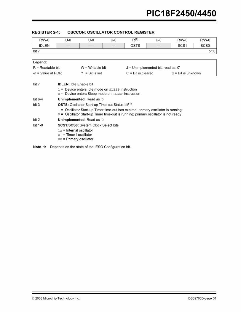
REGISTER 2-1: OSCCON: OSCILLATOR CONTROL REGISTER
R/W-0 U-0 U-0 U-0 R(1) U-0 R/W-0 R/W-0IDLEN � � � OSTS � SCS1 SCS0
bit 7 bit 0
Legend:R = Readable bit W = Writable bit U = Unimplemented bit, read as �0�-n = Value at POR �1� = Bit is set �0� = Bit is cleared x = Bit is unknown
bit 7 IDLEN: Idle Enable bit1 = Device enters Idle mode on SLEEP instruction0 = Device enters Sleep mode on SLEEP instruction
bit 6-4 Unimplemented: Read as �0�bit 3 OSTS: Oscillator Start-up Time-out Status bit(1)
1 = Oscillator Start-up Timer time-out has expired; primary oscillator is running0 = Oscillator Start-up Timer time-out is running; primary oscillator is not ready
bit 2 Unimplemented: Read as �0�bit 1-0 SCS1:SCS0: System Clock Select bits
1x = Internal oscillator01 = Timer1 oscillator00 = Primary oscillator
Note 1: Depends on the state of the IESO Configuration bit.

PIC18F2450/4450
DS39760D-page 32 © 2008 Microchip Technology Inc.
2.5 Effects of Power-Managed Modes on the Various Clock Sources
When PRI_IDLE mode is selected, the designatedprimary oscillator continues to run without interruption.For all other power-managed modes, the oscillatorusing the OSC1 pin is disabled. Unless the USBmodule is enabled, the OSC1 pin (and OSC2 pin ifused by the oscillator) will stop oscillating.
In secondary clock modes (SEC_RUN andSEC_IDLE), the Timer1 oscillator is operating andproviding the device clock. The Timer1 oscillator mayalso run in all power-managed modes if required toclock Timer1.
In internal oscillator modes (RC_RUN and RC_IDLE),the internal oscillator provides the device clock source.The 31 kHz INTRC output can be used directly toprovide the clock and may be enabled to support variousspecial features regardless of the power-managedmode (see Section 18.2 �Watchdog Timer (WDT)�,Section 18.3 �Two-Speed Start-up� and Section 18.4�Fail-Safe Clock Monitor� for more information onWDT, Fail-Safe Clock Monitor and Two-Speed Start-up).
Regardless of the Run or Idle mode selected, the USBclock source will continue to operate. If the device isoperating from a crystal or resonator-based oscillator,that oscillator will continue to clock the USB module.The core and all other modules will switch to the newclock source.
If the Sleep mode is selected, all clock sources arestopped. Since all the transistor switching currentshave been stopped, Sleep mode achieves the lowestcurrent consumption of the device (only leakagecurrents).
Sleep mode should never be invoked while the USBmodule is operating and connected. The only exceptionis when the device has been issued a �Suspend� com-mand over the USB. Once the module has suspendedoperation and shifted to a low-power state, themicrocontroller may be safely put into Sleep mode.
Enabling any on-chip feature that will operate duringSleep will increase the current consumed during Sleep.The INTRC is required to support WDT operation. TheTimer1 oscillator may be operating to support a Real-Time Clock. Other features may be operating that donot require a device clock source (i.e., PSP, INTx pinsand others). Peripherals that may add significantcurrent consumption are listed in Section 21.2 �DCCharacteristics: Power-Down and Supply Current�.
2.6 Power-up DelaysPower-up delays are controlled by two timers, so that noexternal Reset circuitry is required for most applications.The delays ensure that the device is kept in Reset untilthe device power supply is stable under normal circum-stances and the primary clock is operating and stable.For additional information on power-up delays, seeSection 4.5 �Device Reset Timers�.
The first timer is the Power-up Timer (PWRT), whichprovides a fixed delay on power-up (parameter 33,Table 21-10). It is enabled by clearing (= 0) thePWRTEN Configuration bit.
The second timer is the Oscillator Start-up Timer(OST), intended to keep the chip in Reset until thecrystal oscillator is stable (XT and HS modes). TheOST does this by counting 1024 oscillator cyclesbefore allowing the oscillator to clock the device.
When the HSPLL Oscillator mode is selected, thedevice is kept in Reset for an additional 2 ms followingthe HS mode OST delay, so the PLL can lock to theincoming clock frequency.
There is a delay of interval, TCSD (parameter 38,Table 21-10), following POR, while the controllerbecomes ready to execute instructions. This delay runsconcurrently with any other delays. This may be theonly delay that occurs when any of the EC or internaloscillator modes are used as the primary clock source.
TABLE 2-4: OSC1 AND OSC2 PIN STATES IN SLEEP MODE Oscillator Mode OSC1 Pin OSC2 Pin
INTCKO Floating, pulled by external clock At logic low (clock/4 output)INTIO Floating, pulled by external clock Configured as PORTA, bit 6ECIO, ECPIO Floating, pulled by external clock Configured as PORTA, bit 6EC Floating, pulled by external clock At logic low (clock/4 output)XT and HS Feedback inverter disabled at quiescent
voltage levelFeedback inverter disabled at quiescent voltage level
Note: See Table 4-2 in Section 4.0 �Reset� for time-outs due to Sleep and MCLR Reset.

PIC18F2450/4450
© 2008 Microchip Technology Inc. DS39760D-page 33
3.0 POWER-MANAGED MODESPIC18F2450/4450 devices offer a total of sevenoperating modes for more efficient powermanagement. These modes provide a variety ofoptions for selective power conservation in applicationswhere resources may be limited (i.e., battery-powereddevices).
There are three categories of power-managed modes:
� Run modes� Idle modes � Sleep mode
These categories define which portions of the deviceare clocked and sometimes, what speed. The Run andIdle modes may use any of the three available clocksources (primary, secondary or internal oscillator); theSleep mode does not use a clock source.
The power-managed modes include several power-saving features offered on previous PIC®
microcontrollers. One is the clock switching feature,offered in other PIC18 devices, allowing the controllerto use the Timer1 oscillator in place of the primaryoscillator. Also included is the Sleep mode, offered byall PIC microcontrollers, where all device clocks arestopped.
3.1 Selecting Power-Managed ModesSelecting a power-managed mode requires twodecisions: if the CPU is to be clocked or not and theselection of a clock source. The IDLEN bit(OSCCON<7>) controls CPU clocking, while theSCS1:SCS0 bits (OSCCON<1:0>) select the clocksource. The individual modes, bit settings, clock sourcesand affected modules are summarized in Table 3-1.
3.1.1 CLOCK SOURCESThe SCS1:SCS0 bits allow the selection of one of threeclock sources for power-managed modes. They are:
� The primary clock, as defined by the FOSC3:FOSC0 Configuration bits
� The secondary clock (the Timer1 oscillator)� The internal oscillator (for RC modes)
3.1.2 ENTERING POWER-MANAGED MODES
Switching from one power-managed mode to anotherbegins by loading the OSCCON register. TheSCS1:SCS0 bits select the clock source and determinewhich Run or Idle mode is to be used. Changing thesebits causes an immediate switch to the new clocksource, assuming that it is running. The switch mayalso be subject to clock transition delays. These arediscussed in Section 3.1.3 �Clock Transitions andStatus Indicators� and subsequent sections.
Entry to the power-managed Idle or Sleep modes istriggered by the execution of a SLEEP instruction. Theactual mode that results depends on the status of theIDLEN bit.
Depending on the current mode and the mode beingswitched to, a change to a power-managed mode doesnot always require setting all of these bits. Manytransitions may be done by changing the oscillatorselect bits, or changing the IDLEN bit, prior to issuing aSLEEP instruction. If the IDLEN bit is alreadyconfigured correctly, it may only be necessary toperform a SLEEP instruction to switch to the desiredmode.
TABLE 3-1: POWER-MANAGED MODES
ModeOSCCON Bits Module Clocking
Available Clock and Oscillator SourceIDLEN(1) SCS1:SCS0 CPU Peripherals
Sleep 0 N/A Off Off None � all clocks are disabledPRI_RUN N/A 00 Clocked Clocked Primary � all oscillator modes.
This is the normal full-power execution mode.SEC_RUN N/A 01 Clocked Clocked Secondary � Timer1 oscillatorRC_RUN N/A 1x Clocked Clocked Internal oscillator(2)
PRI_IDLE 1 00 Off Clocked Primary � all oscillator modesSEC_IDLE 1 01 Off Clocked Secondary � Timer1 oscillatorRC_IDLE 1 1x Off Clocked Internal oscillator(2)
Note 1: IDLEN reflects its value when the SLEEP instruction is executed.2: Clock is INTRC source.
PIC18F2450/4450
DS39760D-page 34 © 2008 Microchip Technology Inc.
3.1.3 CLOCK TRANSITIONS AND STATUS INDICATORS
The length of the transition between clock sources isthe sum of two cycles of the old clock source and threeto four cycles of the new clock source. This formulaassumes that the new clock source is stable.
Two bits indicate the current clock source and itsstatus. They are:
� OSTS (OSCCON<3>) � T1RUN (T1CON<6>)
In general, only one of these bits will be set while in agiven power-managed mode. When the OSTS bit isset, the primary clock is providing the device clock.When the T1RUN bit is set, the Timer1 oscillator isproviding the clock.
3.1.4 MULTIPLE SLEEP COMMANDSThe power-managed mode that is invoked with theSLEEP instruction is determined by the setting of theIDLEN bit at the time the instruction is executed. Ifanother SLEEP instruction is executed, the device willenter the power-managed mode specified by IDLEN atthat time. If IDLEN has changed, the device will enterthe new power-managed mode specified by the newsetting.
3.2 Run ModesIn the Run modes, clocks to both the core andperipherals are active. The difference between thesemodes is the clock source.
3.2.1 PRI_RUN MODEThe PRI_RUN mode is the normal, full-power execu-tion mode of the microcontroller. This is also the defaultmode upon a device Reset unless Two-Speed Start-upis enabled (see Section 18.3 �Two-Speed Start-up�for details). In this mode, the OSTS bit is set.
3.2.2 SEC_RUN MODEThe SEC_RUN mode is the compatible mode to the�clock switching� feature offered in other PIC18devices. In this mode, the CPU and peripherals areclocked from the Timer1 oscillator. This gives users theoption of lower power consumption while still using ahigh accuracy clock source.
SEC_RUN mode is entered by setting the SCS1:SCS0bits to �01�. The device clock source is switched to theTimer1 oscillator (see Figure 3-1), the primaryoscillator is shut down, the T1RUN bit (T1CON<6>) isset and the OSTS bit is cleared.
Note: Executing a SLEEP instruction does notnecessarily place the device into Sleepmode. It acts as the trigger to place thecontroller into either the Sleep mode, orone of the Idle modes, depending on thesetting of the IDLEN bit.
Note: The Timer1 oscillator should already berunning prior to entering SEC_RUN mode.If the T1OSCEN bit is not set when theSCS1:SCS0 bits are set to �01�, entry toSEC_RUN mode will not occur. If theTimer1 oscillator is enabled but not yetrunning, device clocks will be delayed untilthe oscillator has started. In suchsituations, initial oscillator operation is farfrom stable and unpredictable operationmay result.
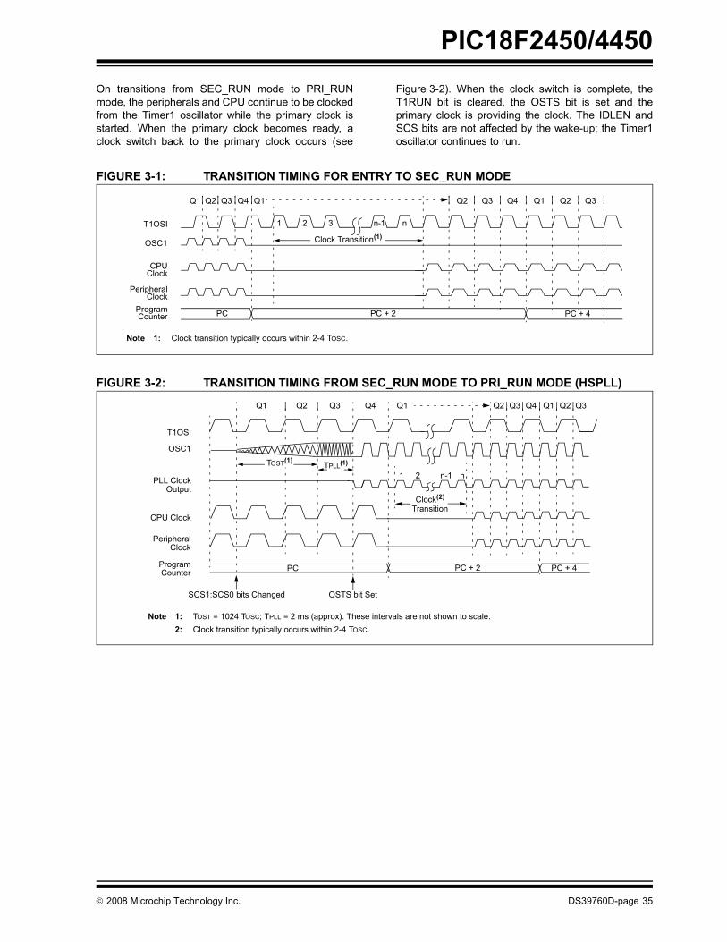
PIC18F2450/4450
© 2008 Microchip Technology Inc. DS39760D-page 35
On transitions from SEC_RUN mode to PRI_RUNmode, the peripherals and CPU continue to be clockedfrom the Timer1 oscillator while the primary clock isstarted. When the primary clock becomes ready, aclock switch back to the primary clock occurs (see
Figure 3-2). When the clock switch is complete, theT1RUN bit is cleared, the OSTS bit is set and theprimary clock is providing the clock. The IDLEN andSCS bits are not affected by the wake-up; the Timer1oscillator continues to run.
FIGURE 3-1: TRANSITION TIMING FOR ENTRY TO SEC_RUN MODE
FIGURE 3-2: TRANSITION TIMING FROM SEC_RUN MODE TO PRI_RUN MODE (HSPLL)
Q4Q3Q2
OSC1
Peripheral
Program
Q1
T1OSI
Q1
Counter
Clock
CPUClock
PC + 2PC
1 2 3 n-1 n
Clock Transition(1)
Q4Q3Q2 Q1 Q3Q2
PC + 4
Note 1: Clock transition typically occurs within 2-4 TOSC.
Q1 Q3 Q4
OSC1
Peripheral
Program PC
T1OSI
PLL Clock
Q1
PC + 4
Q2
Output
Q3 Q4 Q1
CPU Clock
PC + 2
Clock
Counter
Q2 Q2 Q3
Note 1: TOST = 1024 TOSC; TPLL = 2 ms (approx). These intervals are not shown to scale.2: Clock transition typically occurs within 2-4 TOSC.
SCS1:SCS0 bits Changed
TPLL(1)
1 2 n-1 n
Clock(2)
OSTS bit Set
Transition
TOST(1)

PIC18F2450/4450
DS39760D-page 36 © 2008 Microchip Technology Inc.
3.2.3 RC_RUN MODEIn RC_RUN mode, the CPU and peripherals areclocked from the internal oscillator; the primary clock isshut down. When using the INTRC source, this modeprovides the best power conservation of all the Runmodes while still executing code. It works well for userapplications which are not highly timing sensitive or donot require high-speed clocks at all times.
If the primary clock source is the internal oscillator(INTRC), there are no distinguishable differencesbetween the PRI_RUN and RC_RUN modes duringexecution. However, a clock switch delay will occur dur-ing entry to and exit from RC_RUN mode. Therefore, ifthe primary clock source is the internal oscillator, theuse of RC_RUN mode is not recommended.
This mode is entered by setting SCS1 to �1�. Althoughit is ignored, it is recommended that SCS0 also becleared; this is to maintain software compatibility withfuture devices. When the clock source is switched tothe INTRC (see Figure 3-3), the primary oscillator isshut down and the OSTS bit is cleared.
On transitions from RC_RUN mode to PRI_RUN mode,the device continues to be clocked from the INTRCwhile the primary clock is started. When the primaryclock becomes ready, a clock switch to the primaryclock occurs (see Figure 3-4). When the clock switch iscomplete, the OSTS bit is set and the primary clock isproviding the device clock. The IDLEN and SCS bitsare not affected by the switch. The INTRC source willcontinue to run if either the WDT or the Fail-Safe ClockMonitor is enabled.
FIGURE 3-3: TRANSITION TIMING TO RC_RUN MODE
FIGURE 3-4: TRANSITION TIMING FROM RC_RUN MODE TO PRI_RUN MODE
Q4Q3Q2
OSC1
Peripheral
Program
Q1
INTRC
Q1
Counter
Clock
CPUClock
PC + 2PC
1 2 3 n-1 n
Clock Transition(1)
Q4Q3Q2 Q1 Q3Q2
PC + 4
Note 1: Clock transition typically occurs within 2-4 TOSC.
Q1 Q3 Q4
OSC1
Peripheral
Program PC
INTRC
PLL Clock
Q1
PC + 4
Q2
Output
Q3 Q4 Q1
CPU Clock
PC + 2
Clock
Counter
Q2 Q2 Q3
Note 1: TOST = 1024 TOSC; TPLL = 2 ms (approx). These intervals are not shown to scale.2: Clock transition typically occurs within 2-4 TOSC.
SCS1:SCS0 bits Changed
TPLL(1)
1 2 n-1 n
Clock(2)
OSTS bit Set
Transition
TOST(1)

PIC18F2450/4450
© 2008 Microchip Technology Inc. DS39760D-page 37
3.3 Sleep ModeThe power-managed Sleep mode in the PIC18F2450/4450 devices is identical to the legacy Sleep modeoffered in all other PIC microcontrollers. It is entered byclearing the IDLEN bit (the default state on deviceReset) and executing the SLEEP instruction. This shutsdown the selected oscillator (Figure 3-5). All clocksource status bits are cleared.
Entering the Sleep mode from any other mode does notrequire a clock switch. This is because no clocks areneeded once the controller has entered Sleep. If theWDT is selected, the INTRC source will continue tooperate. If the Timer1 oscillator is enabled, it will alsocontinue to run.
When a wake event occurs in Sleep mode (by interrupt,Reset or WDT time-out), the device will not be clockeduntil the clock source selected by the SCS1:SCS0 bitsbecomes ready (see Figure 3-6), or it will be clockedfrom the internal oscillator if either the Two-SpeedStart-up or the Fail-Safe Clock Monitor are enabled(see Section 18.0 �Special Features of the CPU�). Ineither case, the OSTS bit is set when the primary clockis providing the device clocks. The IDLEN and SCS bitsare not affected by the wake-up.
3.4 Idle ModesThe Idle modes allow the controller�s CPU to beselectively shut down while the peripherals continue tooperate. Selecting a particular Idle mode allows usersto further manage power consumption.
If the IDLEN bit is set to �1� when a SLEEP instruction isexecuted, the peripherals will be clocked from the clocksource selected using the SCS1:SCS0 bits; however, theCPU will not be clocked. The clock source status bits arenot affected. Setting IDLEN and executing a SLEEPinstruction provides a quick method of switching from agiven Run mode to its corresponding Idle mode.
If the WDT is selected, the INTRC source will continueto operate. If the Timer1 oscillator is enabled, it will alsocontinue to run.
Since the CPU is not executing instructions, the onlyexits from any of the Idle modes are by interrupt, WDTtime-out or a Reset. When a wake event occurs, CPUexecution is delayed by an interval of TCSD(parameter 38, Table 21-10) while it becomes ready toexecute code. When the CPU begins executing code,it resumes with the same clock source for the currentIdle mode. For example, when waking from RC_IDLEmode, the internal oscillator will clock the CPU andperipherals (in other words, RC_RUN mode). TheIDLEN and SCS bits are not affected by the wake-up.
While in any Idle mode or Sleep mode, a WDT time-outwill result in a WDT wake-up to the Run mode currentlyspecified by the SCS1:SCS0 bits.
FIGURE 3-5: TRANSITION TIMING FOR ENTRY TO SLEEP MODE
FIGURE 3-6: TRANSITION TIMING FOR WAKE FROM SLEEP (HSPLL)
Q4Q3Q2
OSC1
Peripheral
Sleep
Program
Q1Q1
Counter
Clock
CPUClock
PC + 2PC
Q3 Q4 Q1 Q2
OSC1
Peripheral
Program PC
PLL Clock
Q3 Q4
Output
CPU Clock
Q1 Q2 Q3 Q4 Q1 Q2
Clock
Counter PC + 6PC + 4
Q1 Q2 Q3 Q4
Wake Event
Note 1: TOST = 1024 TOSC; TPLL = 2 ms (approx). These intervals are not shown to scale.
TOST(1) TPLL(1)
OSTS bit Set
PC + 2

PIC18F2450/4450
DS39760D-page 38 © 2008 Microchip Technology Inc.
3.4.1 PRI_IDLE MODEThis mode is unique among the three low-power Idlemodes in that it does not disable the primary deviceclock. For timing sensitive applications, this allows forthe fastest resumption of device operation, with itsmore accurate primary clock source, since the clocksource does not have to �warm up� or transition fromanother oscillator.
PRI_IDLE mode is entered from PRI_RUN mode bysetting the IDLEN bit and executing a SLEEPinstruction. If the device is in another Run mode, setIDLEN first, then clear the SCS bits and executeSLEEP. Although the CPU is disabled, the peripheralscontinue to be clocked from the primary clock sourcespecified by the FOSC3:FOSC0 Configuration bits.The OSTS bit remains set (see Figure 3-7).
When a wake event occurs, the CPU is clocked from theprimary clock source. A delay of interval TCSD isrequired between the wake event and when codeexecution starts. This is required to allow the CPU tobecome ready to execute instructions. After the wake-up, the OSTS bit remains set. The IDLEN and SCS bitsare not affected by the wake-up (see Figure 3-8).
3.4.2 SEC_IDLE MODEIn SEC_IDLE mode, the CPU is disabled but theperipherals continue to be clocked from the Timer1oscillator. This mode is entered from SEC_RUN bysetting the IDLEN bit and executing a SLEEPinstruction. If the device is in another Run mode, setIDLEN first, then set SCS1:SCS0 to �01� and executeSLEEP. When the clock source is switched to theTimer1 oscillator, the primary oscillator is shut down,the OSTS bit is cleared and the T1RUN bit is set.
When a wake event occurs, the peripherals continue tobe clocked from the Timer1 oscillator. After an interval ofTCSD following the wake event, the CPU begins execut-ing code being clocked by the Timer1 oscillator. TheIDLEN and SCS bits are not affected by the wake-up;the Timer1 oscillator continues to run (see Figure 3-8).
FIGURE 3-7: TRANSITION TIMING FOR ENTRY TO IDLE MODE
FIGURE 3-8: TRANSITION TIMING FOR WAKE FROM IDLE TO RUN MODE
Note: The Timer1 oscillator should already berunning prior to entering SEC_IDLE mode.If the T1OSCEN bit is not set when theSLEEP instruction is executed, the SLEEPinstruction will be ignored and entry toSEC_IDLE mode will not occur. If theTimer1 oscillator is enabled but not yet run-ning, peripheral clocks will be delayed untilthe oscillator has started. In such situations,initial oscillator operation is far from stableand unpredictable operation may result.
Q1
Peripheral
Program PC PC + 2
OSC1
Q3 Q4 Q1
CPU Clock
Clock
Counter
Q2
OSC1
Peripheral
Program PC
CPU Clock
Q1 Q3 Q4
Clock
Counter
Q2
Wake Event
TCSD

PIC18F2450/4450
© 2008 Microchip Technology Inc. DS39760D-page 39
3.4.3 RC_IDLE MODEIn RC_IDLE mode, the CPU is disabled but the periph-erals continue to be clocked from the internal oscillator,INTRC. This mode allows for controllable powerconservation during Idle periods.
From RC_RUN, this mode is entered by setting theIDLEN bit and executing a SLEEP instruction. If thedevice is in another Run mode, first set IDLEN, then setthe SCS1 bit and execute SLEEP. Although its value isignored, it is recommended that SCS0 also be cleared;this is to maintain software compatibility with futuredevices. When the clock source is switched to theINTRC, the primary oscillator is shut down and theOSTS bit is cleared.
When a wake event occurs, the peripherals continue tobe clocked from the INTRC. After a delay of TCSDfollowing the wake event, the CPU begins executingcode being clocked by the INTRC. The IDLEN and SCSbits are not affected by the wake-up. The INTRC sourcewill continue to run if either the WDT or the Fail-SafeClock Monitor is enabled.
3.5 Exiting Idle and Sleep ModesAn exit from Sleep mode or any of the Idle modes istriggered by an interrupt, a Reset or a WDT time-out.This section discusses the triggers that cause exitsfrom power-managed modes. The clocking subsystemactions are discussed in each of the power-managedmodes (see Section 3.2 �Run Modes�, Section 3.3�Sleep Mode� and Section 3.4 �Idle Modes�).
3.5.1 EXIT BY INTERRUPTAny of the available interrupt sources can cause thedevice to exit from an Idle mode, or the Sleep mode, toa Run mode. To enable this functionality, an interruptsource must be enabled by setting its enable bit in oneof the INTCON or PIE registers. The exit sequence isinitiated when the corresponding interrupt flag bit is set.
On all exits from Idle or Sleep modes by interrupt, codeexecution branches to the interrupt vector if the GIE/GIEH bit (INTCON<7>) is set. Otherwise, code executioncontinues or resumes without branching (seeSection 8.0 �Interrupts�).
A fixed delay of interval, TCSD, following the wakeevent, is required when leaving Sleep and Idle modes.This delay is required for the CPU to prepare for execu-tion. Instruction execution resumes on the first clockcycle following this delay.
3.5.2 EXIT BY WDT TIME-OUTA WDT time-out will cause different actions dependingon which power-managed mode the device is in whenthe time-out occurs.
If the device is not executing code (all Idle modes andSleep mode), the time-out will result in an exit from thepower-managed mode (see Section 3.2 �RunModes� and Section 3.3 �Sleep Mode�). If the deviceis executing code (all Run modes), the time-out willresult in a WDT Reset (see Section 18.2 �WatchdogTimer (WDT)�).
3.5.3 EXIT BY RESETNormally, the device is held in Reset by the OscillatorStart-up Timer (OST) until the primary clock becomesready. At that time, the OSTS bit is set and the devicebegins executing code.
The exit delay time from Reset to the start of codeexecution depends on both the clock sources beforeand after the wake-up and the type of oscillator if thenew clock source is the primary clock. Exit delays aresummarized in Table 3-2.
Code execution can begin before the primary clockbecomes ready. If either the Two-Speed Start-up (seeSection 18.3 �Two-Speed Start-up�) or Fail-SafeClock Monitor (see Section 18.4 �Fail-Safe ClockMonitor�) is enabled, the device may begin executionas soon as the Reset source has cleared. Execution isclocked by the INTRC driven by the internal oscillator.Execution is clocked by the internal oscillator untileither the primary clock becomes ready or a power-managed mode is entered before the primary clockbecomes ready; the primary clock is then shut down.
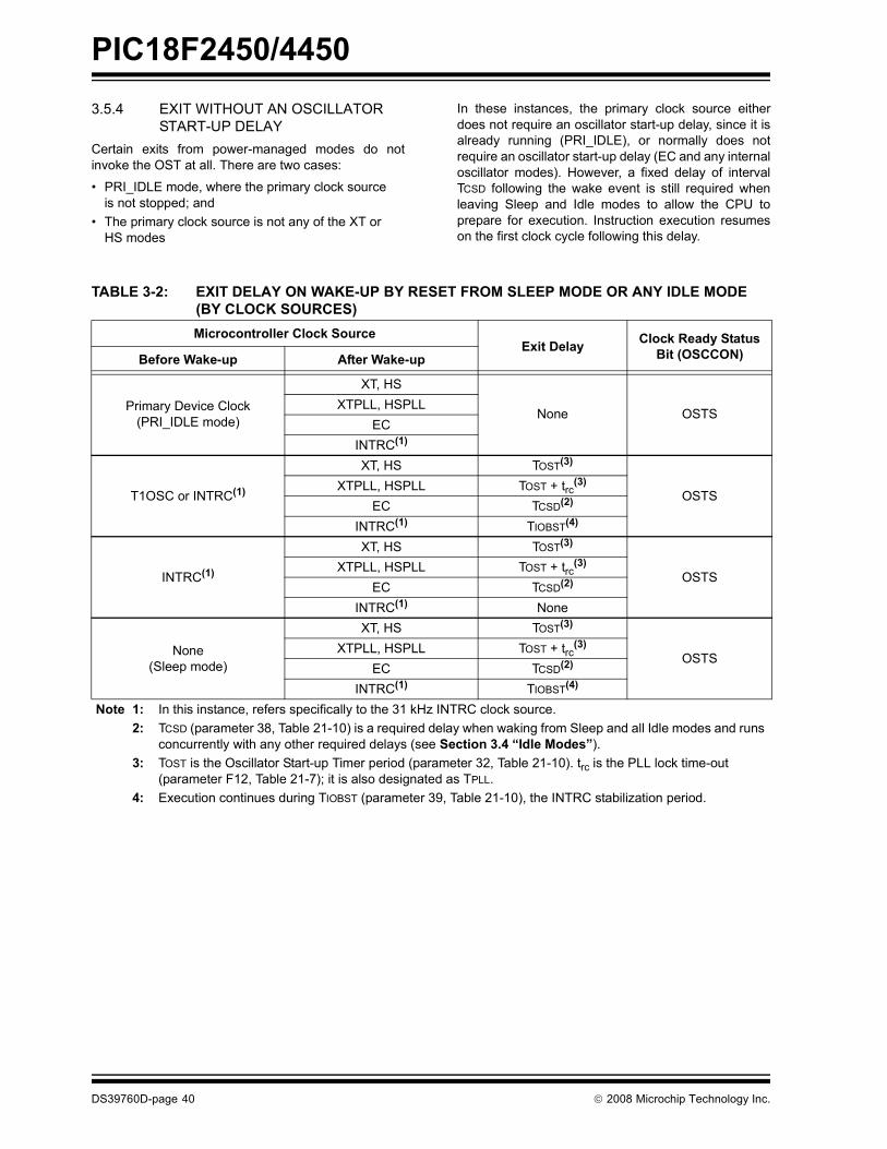
PIC18F2450/4450
DS39760D-page 40 © 2008 Microchip Technology Inc.
3.5.4 EXIT WITHOUT AN OSCILLATOR START-UP DELAY
Certain exits from power-managed modes do notinvoke the OST at all. There are two cases:
� PRI_IDLE mode, where the primary clock source is not stopped; and
� The primary clock source is not any of the XT or HS modes
In these instances, the primary clock source eitherdoes not require an oscillator start-up delay, since it isalready running (PRI_IDLE), or normally does notrequire an oscillator start-up delay (EC and any internaloscillator modes). However, a fixed delay of intervalTCSD following the wake event is still required whenleaving Sleep and Idle modes to allow the CPU toprepare for execution. Instruction execution resumeson the first clock cycle following this delay.
TABLE 3-2: EXIT DELAY ON WAKE-UP BY RESET FROM SLEEP MODE OR ANY IDLE MODE(BY CLOCK SOURCES) Microcontroller Clock Source
Exit Delay Clock Ready Status Bit (OSCCON)Before Wake-up After Wake-up
Primary Device Clock(PRI_IDLE mode)
XT, HS
None OSTSXTPLL, HSPLL
ECINTRC(1)
T1OSC or INTRC(1)
XT, HS TOST(3)
OSTSXTPLL, HSPLL TOST + trc(3)
EC TCSD(2)
INTRC(1) TIOBST(4)
INTRC(1)
XT, HS TOST(3)
OSTSXTPLL, HSPLL TOST + trc(3)
EC TCSD(2)
INTRC(1) None
None(Sleep mode)
XT, HS TOST(3)
OSTSXTPLL, HSPLL TOST + trc(3)
EC TCSD(2)
INTRC(1) TIOBST(4)
Note 1: In this instance, refers specifically to the 31 kHz INTRC clock source.2: TCSD (parameter 38, Table 21-10) is a required delay when waking from Sleep and all Idle modes and runs
concurrently with any other required delays (see Section 3.4 �Idle Modes�).3: TOST is the Oscillator Start-up Timer period (parameter 32, Table 21-10). trc is the PLL lock time-out
(parameter F12, Table 21-7); it is also designated as TPLL.4: Execution continues during TIOBST (parameter 39, Table 21-10), the INTRC stabilization period.

PIC18F2450/4450
© 2008 Microchip Technology Inc. DS39760D-page 41
4.0 RESETThe PIC18F2450/4450 devices differentiate betweenvarious kinds of Reset:
a) Power-on Reset (POR) b) MCLR Reset during normal operationc) MCLR Reset during power-managed modes d) Watchdog Timer (WDT) Reset (during
execution)e) Programmable Brown-out Reset (BOR) f) RESET Instructiong) Stack Full Reseth) Stack Underflow Reset
This section discusses Resets generated by MCLR,POR and BOR, and covers the operation of the variousstart-up timers. Stack Reset events are covered inSection 5.1.2.4 �Stack Full and Underflow Resets�.WDT Resets are covered in Section 18.2 �WatchdogTimer (WDT)�.
A simplified block diagram of the on-chip Reset circuitis shown in Figure 4-1.
4.1 RCON RegisterDevice Reset events are tracked through the RCONregister (Register 4-1). The lower five bits of theregister indicate that a specific Reset event hasoccurred. In most cases, these bits can only be clearedby the event and must be set by the application afterthe event. The state of these flag bits, taken together,can be read to indicate the type of Reset that justoccurred. This is described in more detail inSection 4.6 �Reset State of Registers�.
The RCON register also has control bits for settinginterrupt priority (IPEN) and software control of theBOR (SBOREN). Interrupt priority is discussed inSection 8.0 �Interrupts�. BOR is covered inSection 4.4 �Brown-out Reset (BOR)�.
FIGURE 4-1: SIMPLIFIED BLOCK DIAGRAM OF ON-CHIP RESET CIRCUIT
S
R Q
External Reset
MCLR
VDD
OSC1
WDTTime-out
VDD RiseDetect
OST/PWRT
INTRC(1)
POR Pulse
OST10-Bit Ripple Counter
PWRT
Chip_Reset
11-Bit Ripple Counter
Enable OST(2)
Enable PWRT
Note 1: This is the INTRC source from the internal oscillator and is separate from the RC oscillator of the CLKI pin.2: See Table 4-2 for time-out situations.
Brown-outReset
BOREN
RESET Instruction
StackPointer
Stack Full/Underflow Reset
Sleep( )_IDLE
1024 Cycles
65.5 ms32 μs
MCLRE

PIC18F2450/4450
DS39760D-page 42 © 2008 Microchip Technology Inc.
REGISTER 4-1: RCON: RESET CONTROL REGISTER
R/W-0 R/W-1(1) U-0 R/W-1 R-1 R-1 R/W-0(2) R/W-0
IPEN SBOREN � RI TO PD POR BORbit 7 bit 0
Legend:R = Readable bit W = Writable bit U = Unimplemented bit, read as �0�-n = Value at POR �1� = Bit is set �0� = Bit is cleared x = Bit is unknown
bit 7 IPEN: Interrupt Priority Enable bit 1 = Enable priority levels on interrupts0 = Disable priority levels on interrupts (PIC16CXXX Compatibility mode)
bit 6 SBOREN: BOR Software Enable bit(1) If BOREN1:BOREN0 = 01:1 = BOR is enabled0 = BOR is disabledIf BOREN1:BOREN0 = 00, 10 or 11:Bit is disabled and read as �0�.
bit 5 Unimplemented: Read as �0�bit 4 RI: RESET Instruction Flag bit
1 = The RESET instruction was not executed (set by firmware only)0 = The RESET instruction was executed causing a device Reset (must be set in software after a
Brown-out Reset occurs)bit 3 TO: Watchdog Time-out Flag bit
1 = Set by power-up, CLRWDT instruction or SLEEP instruction 0 = A WDT time-out occurred
bit 2 PD: Power-Down Detection Flag bit 1 = Set by power-up or by the CLRWDT instruction 0 = Set by execution of the SLEEP instruction
bit 1 POR: Power-on Reset Status bit(2) 1 = A Power-on Reset has not occurred (set by firmware only)0 = A Power-on Reset occurred (must be set in software after a Power-on Reset occurs)
bit 0 BOR: Brown-out Reset Status bit1 = A Brown-out Reset has not occurred (set by firmware only)0 = A Brown-out Reset occurred (must be set in software after a Brown-out Reset occurs)
Note 1: If SBOREN is enabled, its Reset state is �1�; otherwise, it is �0�.2: The actual Reset value of POR is determined by the type of device Reset. See the notes following this
register and Section 4.6 �Reset State of Registers� for additional information.
Note 1: It is recommended that the POR bit be set after a Power-on Reset has been detected so that subsequentPower-on Resets may be detected.
2: Brown-out Reset is said to have occurred when BOR is �0� and POR is �1� (assuming that POR was set to�1� by software immediately after a Power-on Rest).

PIC18F2450/4450
© 2008 Microchip Technology Inc. DS39760D-page 43
4.2 Master Clear Reset (MCLR)The MCLR pin provides a method for triggering anexternal Reset of the device. A Reset is generated byholding the pin low. These devices have a noise filter inthe MCLR Reset path which detects and ignores smallpulses.
The MCLR pin is not driven low by any internal Resets,including the WDT.
In PIC18F2450/4450 devices, the MCLR input can bedisabled with the MCLRE Configuration bit. WhenMCLR is disabled, the pin becomes a digital input. SeeSection 9.5 �PORTE, TRISE and LATE Registers�for more information.
4.3 Power-on Reset (POR)A Power-on Reset pulse is generated on-chipwhenever VDD rises above a certain threshold. Thisallows the device to start in the initialized state whenVDD is adequate for operation.
To take advantage of the POR circuitry, tie the MCLR pinthrough a resistor (1 kΩ to 10 kΩ) to VDD. This willeliminate external RC components usually needed tocreate a Power-on Reset delay. A minimum rise rate forVDD is specified (parameter D004, Section269 �DCCharacteristics�). For a slow rise time, see Figure 4-2.
When the device starts normal operation (i.e., exits theReset condition), device operating parameters (volt-age, frequency, temperature, etc.) must be met toensure operation. If these conditions are not met, thedevice must be held in Reset until the operatingconditions are met.
POR events are captured by the POR bit (RCON<1>).The state of the bit is set to �0� whenever a Power-onReset occurs; it does not change for any other Resetevent. POR is not reset to �1� by any hardware event.To capture multiple events, the user manually resetsthe bit to �1� in software following any Power-on Reset.
FIGURE 4-2: EXTERNAL POWER-ON RESET CIRCUIT (FOR SLOW VDD POWER-UP)
Note 1: External Power-on Reset circuit is requiredonly if the VDD power-up slope is too slow.The diode D helps discharge the capacitorquickly when VDD powers down.
2: R < 40 kΩ is recommended to make sure thatthe voltage drop across R does not violatethe device�s electrical specification.
3: R1 ≥ 1 kΩ will limit any current flowing intoMCLR from external capacitor C, in the eventof MCLR/VPP pin breakdown, due to Electro-static Discharge (ESD) or ElectricalOverstress (EOS).
C
R1RD
VDD
MCLR
PIC18FXXXX
VDD

PIC18F2450/4450
DS39760D-page 44 © 2008 Microchip Technology Inc.
4.4 Brown-out Reset (BOR)PIC18F2450/4450 devices implement a BOR circuitthat provides the user with a number of configurationand power-saving options. The BOR is controlled bythe BORV1:BORV0 and BOREN1:BOREN0Configuration bits. There are a total of four BORconfigurations which are summarized in Table 4-1.
The BOR threshold is set by the BORV1:BORV0 bits. IfBOR is enabled (any values of BOREN1:BOREN0except �00�), any drop of VDD below VBOR (parameterD005, Section 269 �DC Characteristics: SupplyVoltage�) for greater than TBOR (parameter 35,Table 21-10) will reset the device. A Reset may or maynot occur if VDD falls below VBOR for less than TBOR.The chip will remain in Brown-out Reset until VDD risesabove VBOR.
If the Power-up Timer is enabled, it will be invoked afterVDD rises above VBOR; it then will keep the chip inReset for an additional time delay, TPWRT(parameter 33, Table 21-10). If VDD drops below VBORwhile the Power-up Timer is running, the chip will goback into a Brown-out Reset and the Power-up Timerwill be initialized. Once VDD rises above VBOR, thePower-up Timer will execute the additional time delay.
BOR and the Power-on Timer (PWRT) areindependently configured. Enabling BOR Reset doesnot automatically enable the PWRT.
4.4.1 SOFTWARE ENABLED BORWhen BOREN1:BOREN0 = 01, the BOR can beenabled or disabled by the user in software. This isdone with the control bit, SBOREN (RCON<6>).Setting SBOREN enables the BOR to function aspreviously described. Clearing SBOREN disables theBOR entirely. The SBOREN bit operates only in thismode; otherwise, it is read as �0�.
Placing the BOR under software control gives the userthe additional flexibility of tailoring the application to itsenvironment without having to reprogram the device tochange BOR configuration. It also allows the user totailor device power consumption in software by eliminat-ing the incremental current that the BOR consumes.While the BOR current is typically very small, it may havesome impact in low-power applications.
4.4.2 DETECTING BORWhen Brown-out Reset is enabled, the BOR bit alwaysresets to �0� on any Brown-out Reset or Power-onReset event. This makes it difficult to determine if aBrown-out Reset event has occurred just by readingthe state of BOR alone. A more reliable method is tosimultaneously check the state of both POR and BOR.This assumes that the POR bit is reset to �1� in softwareimmediately after any Power-on Reset event. IF BORis �0� while POR is �1�, it can be reliably assumed that aBrown-out Reset event has occurred.
4.4.3 DISABLING BOR IN SLEEP MODEWhen BOREN1:BOREN0 = 10, the BOR remainsunder hardware control and operates as previouslydescribed. Whenever the device enters Sleep mode,however, the BOR is automatically disabled. When thedevice returns to any other operating mode, BOR isautomatically re-enabled.
This mode allows for applications to recover frombrown-out situations, while actively executing code,when the device requires BOR protection the most. Atthe same time, it saves additional power in Sleep modeby eliminating the small incremental BOR current.
TABLE 4-1: BOR CONFIGURATIONS
Note: Even when BOR is under software control,the BOR Reset voltage level is still set bythe BORV1:BORV0 Configuration bits. Itcannot be changed in software.
BOR Configuration Status of SBOREN
(RCON<6>)BOR Operation
BOREN1 BOREN0
0 0 Unavailable BOR disabled; must be enabled by reprogramming the Configuration bits.0 1 Available BOR enabled in software; operation controlled by SBOREN.1 0 Unavailable BOR enabled in hardware in Run and Idle modes, disabled during
Sleep mode.1 1 Unavailable BOR enabled in hardware; must be disabled by reprogramming the
Configuration bits.

PIC18F2450/4450
© 2008 Microchip Technology Inc. DS39760D-page 45
4.5 Device Reset TimersPIC18F2450/4450 devices incorporate three separateon-chip timers that help regulate the Power-on Resetprocess. Their main function is to ensure that thedevice clock is stable before code is executed. Thesetimers are:
� Power-up Timer (PWRT)� Oscillator Start-up Timer (OST)� PLL Lock Time-out
4.5.1 POWER-UP TIMER (PWRT)The Power-up Timer (PWRT) of the PIC18F2450/4450devices is an 11-bit counter which uses the INTRCsource as the clock input. This yields an approximatetime interval of 2048 x 32 μs = 65.6 ms. While thePWRT is counting, the device is held in Reset.
The power-up time delay depends on the INTRC clockand will vary from chip to chip due to temperature andprocess variation. See DC parameter 33 (Table 21-10)for details.
The PWRT is enabled by clearing the PWRTENConfiguration bit.
4.5.2 OSCILLATOR START-UP TIMER (OST)
The Oscillator Start-up Timer (OST) provides a1024 oscillator cycle (from OSC1 input) delay after thePWRT delay is over (parameter 33, Table 21-10). Thisensures that the crystal oscillator or resonator hasstarted and stabilized.
The OST time-out is invoked only for XT, HS andHSPLL modes and only on Power-on Reset or on exitfrom most power-managed modes.
4.5.3 PLL LOCK TIME-OUTWith the PLL enabled in its PLL mode, the time-outsequence following a Power-on Reset is slightly differ-ent from other oscillator modes. A separate timer isused to provide a fixed time-out that is sufficient for thePLL to lock to the main oscillator frequency. This PLLlock time-out (TPLL) is typically 2 ms and follows theoscillator start-up time-out.
4.5.4 TIME-OUT SEQUENCEOn power-up, the time-out sequence is as follows:
1. After the POR condition has cleared, PWRTtime-out is invoked (if enabled).
2. Then, the OST is activated.
The total time-out will vary based on oscillator configu-ration and the status of the PWRT. Figure 4-3,Figure 4-4, Figure 4-5, Figure 4-6 and Figure 4-7 alldepict time-out sequences on power-up, with thePower-up Timer enabled and the device operating inHS Oscillator mode. Figure 4-3 through Figure 4-6 alsoapply to devices operating in XT mode. For devices inRC mode and with the PWRT disabled, on the otherhand, there will be no time-out at all.
Since the time-outs occur from the POR pulse, if MCLRis kept low long enough, all time-outs will expire.Bringing MCLR high will begin execution immediately(Figure 4-5). This is useful for testing purposes or tosynchronize more than one PIC18FXXXX deviceoperating in parallel.
TABLE 4-2: TIME-OUT IN VARIOUS SITUATIONS
OscillatorConfiguration
Power-up(2) and Brown-out Exit from Power-Managed ModePWRTEN = 0 PWRTEN = 1
HS, XT 66 ms(1) + 1024 TOSC 1024 TOSC 1024 TOSC
HSPLL, XTPLL 66 ms(1) + 1024 TOSC + 2 ms(2) 1024 TOSC + 2 ms(2) 1024 TOSC + 2 ms(2)
EC, ECIO 66 ms(1) � �ECPLL, ECPIO 66 ms(1) + 2 ms(2) 2 ms(2) 2 ms(2)
INTIO, INTCKO 66 ms(1) � �INTHS, INTXT 66 ms(1) + 1024 TOSC 1024 TOSC 1024 TOSC
Note 1: 66 ms (65.5 ms) is the nominal Power-up Timer (PWRT) delay.2: 2 ms is the nominal time required for the PLL to lock.
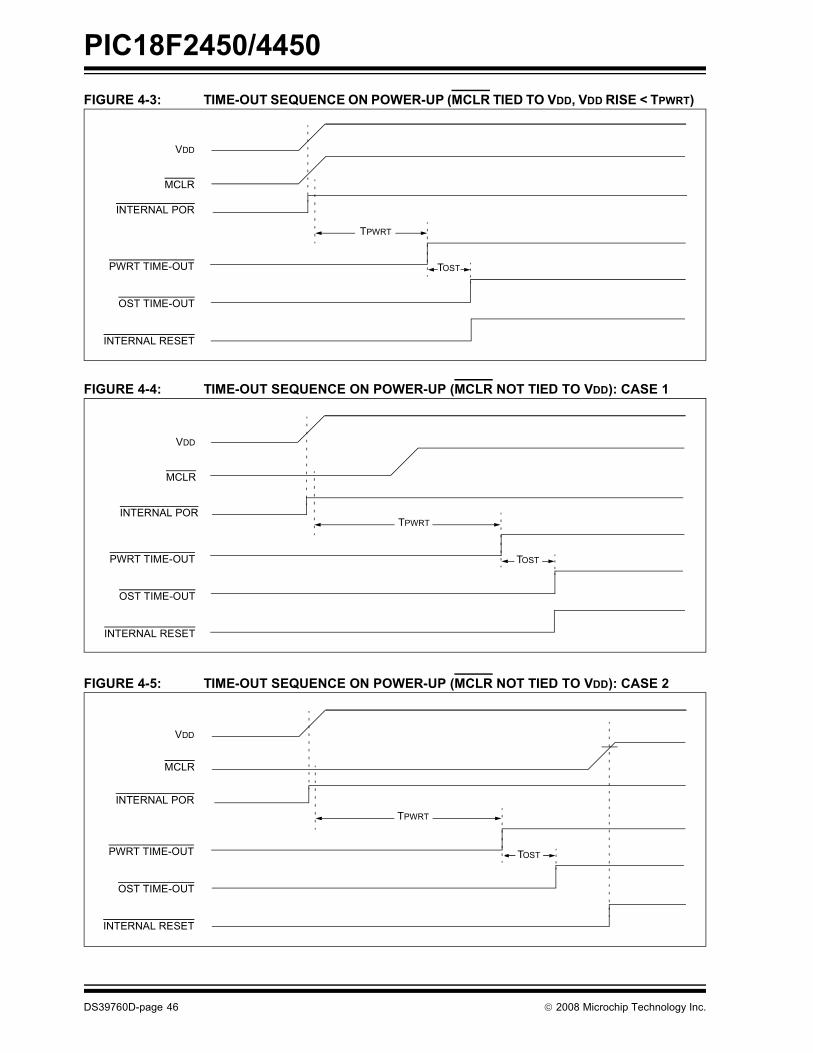
PIC18F2450/4450
DS39760D-page 46 © 2008 Microchip Technology Inc.
FIGURE 4-3: TIME-OUT SEQUENCE ON POWER-UP (MCLR TIED TO VDD, VDD RISE < TPWRT)
FIGURE 4-4: TIME-OUT SEQUENCE ON POWER-UP (MCLR NOT TIED TO VDD): CASE 1
FIGURE 4-5: TIME-OUT SEQUENCE ON POWER-UP (MCLR NOT TIED TO VDD): CASE 2
TPWRT
TOST
VDD
MCLR
INTERNAL POR
PWRT TIME-OUT
OST TIME-OUT
INTERNAL RESET
TPWRT
TOST
VDD
MCLR
INTERNAL POR
PWRT TIME-OUT
OST TIME-OUT
INTERNAL RESET
VDD
MCLR
INTERNAL POR
PWRT TIME-OUT
OST TIME-OUT
INTERNAL RESET
TPWRT
TOST
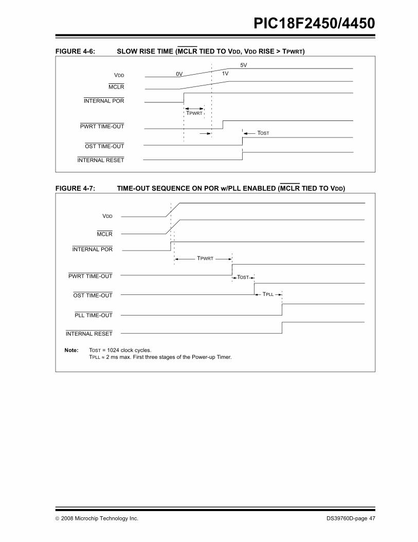
PIC18F2450/4450
© 2008 Microchip Technology Inc. DS39760D-page 47
FIGURE 4-6: SLOW RISE TIME (MCLR TIED TO VDD, VDD RISE > TPWRT)
FIGURE 4-7: TIME-OUT SEQUENCE ON POR w/PLL ENABLED (MCLR TIED TO VDD)
VDD
MCLR
INTERNAL POR
PWRT TIME-OUT
OST TIME-OUT
INTERNAL RESET
0V 1V5V
TPWRT
TOST
TPWRT
TOST
VDD
MCLR
INTERNAL POR
PWRT TIME-OUT
OST TIME-OUT
INTERNAL RESET
PLL TIME-OUT
TPLL
Note: TOST = 1024 clock cycles.TPLL ≈ 2 ms max. First three stages of the Power-up Timer.

PIC18F2450/4450
DS39760D-page 48 © 2008 Microchip Technology Inc.
4.6 Reset State of RegistersMost registers are unaffected by a Reset. Their statusis unknown on POR and unchanged by all otherResets. The other registers are forced to a �Resetstate� depending on the type of Reset that occurred.
Most registers are not affected by a WDT wake-up,since this is viewed as the resumption of normal oper-ation. Status bits from the RCON register, RI, TO, PD,
POR and BOR, are set or cleared differently in differentReset situations as indicated in Table 4-3. These bitsare used in software to determine the nature of theReset.
Table 4-4 describes the Reset states for all of theSpecial Function Registers. These are categorized byPower-on and Brown-out Resets, Master Clear andWDT Resets and WDT wake-ups.
TABLE 4-3: STATUS BITS, THEIR SIGNIFICANCE AND THE INITIALIZATION CONDITION FOR RCON REGISTER
Condition Program Counter
RCON Register STKPTR Register
SBOREN RI TO PD POR BOR STKFUL STKUNF
Power-on Reset 0000h 1 1 1 1 0 0 0 0
RESET instruction 0000h u(2) 0 u u u u u u
Brown-out Reset 0000h u(2) 1 1 1 u 0 u u
MCLR Reset during power-managed Run modes
0000h u(2) u 1 u u u u u
MCLR Reset during power-managed Idle modes and Sleep mode
0000h u(2) u 1 0 u u u u
WDT time-out during full-power or power-managed Run modes
0000h u(2) u 0 u u u u u
MCLR Reset during full-power execution
0000h u(2) u u u u u u u
Stack Full Reset (STVREN = 1) 0000h u(2) u u u u u 1 u
Stack Underflow Reset (STVREN = 1)
0000h u(2) u u u u u u 1
Stack Underflow Error (not an actual Reset, STVREN = 0)
0000h u(2) u u u u u u 1
WDT time-out during power-managed Idle or Sleep modes
PC + 2 u(2) u 0 0 u u u u
Interrupt exit from power-managed modes
PC + 2(1) u(2) u u 0 u u u u
Legend: u = unchangedNote 1: When the wake-up is due to an interrupt and the GIEH or GIEL bit is set, the PC is loaded with the
interrupt vector (008h or 0018h).2: Reset state is �1� for POR and unchanged for all other Resets when software BOR is enabled
(BOREN1:BOREN0 Configuration bits = 01 and SBOREN = 1); otherwise, the Reset state is �0�.

PIC18F2450/4450
© 2008 Microchip Technology Inc. DS39760D-page 49
TABLE 4-4: INITIALIZATION CONDITIONS FOR ALL REGISTERS
Register Applicable Devices Power-on Reset,Brown-out Reset
MCLR Resets,WDT Reset,
RESET Instruction,Stack Resets
Wake-up via WDT or Interrupt
TOSU 2450 4450 ---0 0000 ---0 0000 ---0 uuuu(1)
TOSH 2450 4450 0000 0000 0000 0000 uuuu uuuu(1)
TOSL 2450 4450 0000 0000 0000 0000 uuuu uuuu(1)
STKPTR 2450 4450 00-0 0000 uu-0 0000 uu-u uuuu(1)
PCLATU 2450 4450 ---0 0000 ---0 0000 ---u uuuu
PCLATH 2450 4450 0000 0000 0000 0000 uuuu uuuu
PCL 2450 4450 0000 0000 0000 0000 PC + 2(3)
TBLPTRU 2450 4450 --00 0000 --00 0000 --uu uuuu
TBLPTRH 2450 4450 0000 0000 0000 0000 uuuu uuuu
TBLPTRL 2450 4450 0000 0000 0000 0000 uuuu uuuu
TABLAT 2450 4450 0000 0000 0000 0000 uuuu uuuu
PRODH 2450 4450 xxxx xxxx uuuu uuuu uuuu uuuu
PRODL 2450 4450 xxxx xxxx uuuu uuuu uuuu uuuu
INTCON 2450 4450 0000 000x 0000 000u uuuu uuuu(2)
INTCON2 2450 4450 1111 -1-1 1111 -1-1 uuuu -u-u(2)
INTCON3 2450 4450 11-0 0-00 11-0 0-00 uu-u u-uu(2)
INDF0 2450 4450 N/A N/A N/APOSTINC0 2450 4450 N/A N/A N/APOSTDEC0 2450 4450 N/A N/A N/APREINC0 2450 4450 N/A N/A N/APLUSW0 2450 4450 N/A N/A N/AFSR0H 2450 4450 ---- 0000 ---- 0000 ---- uuuu
FSR0L 2450 4450 xxxx xxxx uuuu uuuu uuuu uuuu
WREG 2450 4450 xxxx xxxx uuuu uuuu uuuu uuuu
INDF1 2450 4450 N/A N/A N/APOSTINC1 2450 4450 N/A N/A N/APOSTDEC1 2450 4450 N/A N/A N/APREINC1 2450 4450 N/A N/A N/APLUSW1 2450 4450 N/A N/A N/AFSR1H 2450 4450 ---- 0000 ---- 0000 ---- uuuu
FSR1L 2450 4450 xxxx xxxx uuuu uuuu uuuu uuuu
BSR 2450 4450 ---- 0000 ---- 0000 ---- uuuu
Legend: u = unchanged, x = unknown, - = unimplemented bit, read as �0�, q = value depends on condition.Shaded cells indicate conditions do not apply for the designated device.
Note 1: When the wake-up is due to an interrupt and the GIEL or GIEH bit is set, the TOSU, TOSH and TOSL are updated with the current value of the PC. The STKPTR is modified to point to the next location in the hardware stack.
2: One or more bits in the INTCONx or PIRx registers will be affected (to cause wake-up).3: When the wake-up is due to an interrupt and the GIEL or GIEH bit is set, the PC is loaded with the
interrupt vector (0008h or 0018h).4: See Table 4-3 for Reset value for specific condition.5: PORTA<6>, LATA<6> and TRISA<6> are enabled depending on the oscillator mode selected. When not
enabled as PORTA pins, they are disabled and read �0�.

PIC18F2450/4450
DS39760D-page 50 © 2008 Microchip Technology Inc.
INDF2 2450 4450 N/A N/A N/APOSTINC2 2450 4450 N/A N/A N/APOSTDEC2 2450 4450 N/A N/A N/APREINC2 2450 4450 N/A N/A N/APLUSW2 2450 4450 N/A N/A N/AFSR2H 2450 4450 ---- 0000 ---- 0000 ---- uuuu
FSR2L 2450 4450 xxxx xxxx uuuu uuuu uuuu uuuu
STATUS 2450 4450 ---x xxxx ---u uuuu ---u uuuu
TMR0H 2450 4450 0000 0000 0000 0000 uuuu uuuu
TMR0L 2450 4450 xxxx xxxx uuuu uuuu uuuu uuuu
T0CON 2450 4450 1111 1111 1111 1111 uuuu uuuu
OSCCON 2450 4450 0--- q-00 0--- 0-q0 u--- u-qu
HLVDCON 2450 4450 0-00 0101 0-00 0101 u-uu uuuu
WDTCON 2450 4450 ---- ---0 ---- ---0 ---- ---u
RCON(4) 2450 4450 0q-1 11q0 0q-q qquu uq-u qquu
TMR1H 2450 4450 xxxx xxxx uuuu uuuu uuuu uuuu
TMR1L 2450 4450 xxxx xxxx uuuu uuuu uuuu uuuu
T1CON 2450 4450 0000 0000 u0uu uuuu uuuu uuuu
TMR2 2450 4450 0000 0000 0000 0000 uuuu uuuu
PR2 2450 4450 1111 1111 1111 1111 1111 1111
T2CON 2450 4450 -000 0000 -000 0000 -uuu uuuu
ADRESH 2450 4450 xxxx xxxx uuuu uuuu uuuu uuuu
ADRESL 2450 4450 xxxx xxxx uuuu uuuu uuuu uuuu
ADCON0 2450 4450 --00 0000 --00 0000 --uu uuuu
ADCON1 2450 4450 --00 qqqq --00 qqqq --uu uuuu
ADCON2 2450 4450 0-00 0000 0-00 0000 u-uu uuuu
CCPR1H 2450 4450 xxxx xxxx uuuu uuuu uuuu uuuu
CCPR1L 2450 4450 xxxx xxxx uuuu uuuu uuuu uuuu
CCP1CON 2450 4450 --00 0000 --00 0000 --uu uuuu
BAUDCON 2450 4450 01-0 0-00 01-0 0-00 uu-u u-uu
SPBRG 2450 4450 0000 0000 0000 0000 uuuu uuuu
RCREG 2450 4450 0000 0000 0000 0000 uuuu uuuu
TABLE 4-4: INITIALIZATION CONDITIONS FOR ALL REGISTERS (CONTINUED)
Register Applicable Devices Power-on Reset,Brown-out Reset
MCLR Resets,WDT Reset,
RESET Instruction,Stack Resets
Wake-up via WDT or Interrupt
Legend: u = unchanged, x = unknown, - = unimplemented bit, read as �0�, q = value depends on condition.Shaded cells indicate conditions do not apply for the designated device.
Note 1: When the wake-up is due to an interrupt and the GIEL or GIEH bit is set, the TOSU, TOSH and TOSL are updated with the current value of the PC. The STKPTR is modified to point to the next location in the hardware stack.
2: One or more bits in the INTCONx or PIRx registers will be affected (to cause wake-up).3: When the wake-up is due to an interrupt and the GIEL or GIEH bit is set, the PC is loaded with the
interrupt vector (0008h or 0018h).4: See Table 4-3 for Reset value for specific condition.5: PORTA<6>, LATA<6> and TRISA<6> are enabled depending on the oscillator mode selected. When not
enabled as PORTA pins, they are disabled and read �0�.
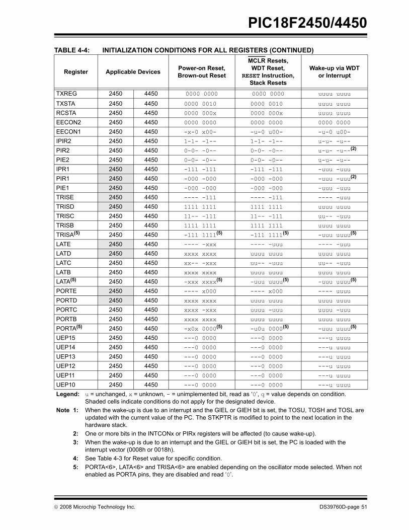
PIC18F2450/4450
© 2008 Microchip Technology Inc. DS39760D-page 51
TXREG 2450 4450 0000 0000 0000 0000 uuuu uuuu
TXSTA 2450 4450 0000 0010 0000 0010 uuuu uuuu
RCSTA 2450 4450 0000 000x 0000 000x uuuu uuuu
EECON2 2450 4450 0000 0000 0000 0000 0000 0000
EECON1 2450 4450 -x-0 x00- -u-0 u00- -u-0 u00-
IPIR2 2450 4450 1-1- -1-- 1-1- -1-- u-u- -u--
PIR2 2450 4450 0-0- -0-- 0-0- -0-- u-u- -u--(2)
PIE2 2450 4450 0-0- -0-- 0-0- -0-- u-u- -u--
IPR1 2450 4450 -111 -111 -111 -111 -uuu -uuu
PIR1 2450 4450 -000 -000 -000 -000 -uuu -uuu(2)
PIE1 2450 4450 -000 -000 -000 -000 -uuu -uuu
TRISE 2450 4450 ---- -111 ---- -111 ---- -uuu
TRISD 2450 4450 1111 1111 1111 1111 uuuu uuuu
TRISC 2450 4450 11-- -111 11-- -111 uu-- -uuu
TRISB 2450 4450 1111 1111 1111 1111 uuuu uuuu
TRISA(5) 2450 4450 -111 1111(5) -111 1111(5) -uuu uuuu(5)
LATE 2450 4450 ---- -xxx ---- -uuu ---- -uuu
LATD 2450 4450 xxxx xxxx uuuu uuuu uuuu uuuu
LATC 2450 4450 xx-- -xxx uu-- -uuu uu-- -uuu
LATB 2450 4450 xxxx xxxx uuuu uuuu uuuu uuuu
LATA(5) 2450 4450 -xxx xxxx(5) -uuu uuuu(5) -uuu uuuu(5)
PORTE 2450 4450 ---- x000 ---- x000 ---- uuuu
PORTD 2450 4450 xxxx xxxx uuuu uuuu uuuu uuuu
PORTC 2450 4450 xxxx -xxx uuuu -uuu uuuu -uuu
PORTB 2450 4450 xxxx xxxx uuuu uuuu uuuu uuuu
PORTA(5) 2450 4450 -x0x 0000(5) -u0u 0000(5) -uuu uuuu(5)
UEP15 2450 4450 ---0 0000 ---0 0000 ---u uuuu
UEP14 2450 4450 ---0 0000 ---0 0000 ---u uuuu
UEP13 2450 4450 ---0 0000 ---0 0000 ---u uuuu
UEP12 2450 4450 ---0 0000 ---0 0000 ---u uuuu
UEP11 2450 4450 ---0 0000 ---0 0000 ---u uuuu
UEP10 2450 4450 ---0 0000 ---0 0000 ---u uuuu
TABLE 4-4: INITIALIZATION CONDITIONS FOR ALL REGISTERS (CONTINUED)
Register Applicable Devices Power-on Reset,Brown-out Reset
MCLR Resets,WDT Reset,
RESET Instruction,Stack Resets
Wake-up via WDT or Interrupt
Legend: u = unchanged, x = unknown, - = unimplemented bit, read as �0�, q = value depends on condition.Shaded cells indicate conditions do not apply for the designated device.
Note 1: When the wake-up is due to an interrupt and the GIEL or GIEH bit is set, the TOSU, TOSH and TOSL are updated with the current value of the PC. The STKPTR is modified to point to the next location in the hardware stack.
2: One or more bits in the INTCONx or PIRx registers will be affected (to cause wake-up).3: When the wake-up is due to an interrupt and the GIEL or GIEH bit is set, the PC is loaded with the
interrupt vector (0008h or 0018h).4: See Table 4-3 for Reset value for specific condition.5: PORTA<6>, LATA<6> and TRISA<6> are enabled depending on the oscillator mode selected. When not
enabled as PORTA pins, they are disabled and read �0�.

PIC18F2450/4450
DS39760D-page 52 © 2008 Microchip Technology Inc.
UEP9 2450 4450 ---0 0000 ---0 0000 ---u uuuu
UEP8 2450 4450 ---0 0000 ---0 0000 ---u uuuu
UEP7 2450 4450 ---0 0000 ---0 0000 ---u uuuu
UEP6 2450 4450 ---0 0000 ---0 0000 ---u uuuu
UEP5 2450 4450 ---0 0000 ---0 0000 ---u uuuu
UEP4 2450 4450 ---0 0000 ---0 0000 ---u uuuu
UEP3 2450 4450 ---0 0000 ---0 0000 ---u uuuu
UEP2 2450 4450 ---0 0000 ---0 0000 ---u uuuu
UEP1 2450 4450 ---0 0000 ---0 0000 ---u uuuu
UEP0 2450 4450 ---0 0000 ---0 0000 ---u uuuu
UCFG 2450 4450 00-0 0000 00-0 0000 uu-u uuuu
UADDR 2450 4450 -000 0000 -000 0000 -uuu uuuu
UCON 2450 4450 -0x0 000- -0x0 000- -uuu uuu-
USTAT 2450 4450 -xxx xxx- -xxx xxx- -uuu uuu-
UEIE 2450 4450 0--0 0000 0--0 0000 u--u uuuu
UEIR 2450 4450 0--0 0000 0--0 0000 u--u uuuu
UIE 2450 4450 -000 0000 -000 0000 -uuu uuuu
UIR 2450 4450 -000 0000 -000 0000 -uuu uuuu
UFRMH 2450 4450 ---- -xxx ---- -xxx ---- -uuu
UFRML 2450 4450 xxxx xxxx xxxx xxxx uuuu uuuu
TABLE 4-4: INITIALIZATION CONDITIONS FOR ALL REGISTERS (CONTINUED)
Register Applicable Devices Power-on Reset,Brown-out Reset
MCLR Resets,WDT Reset,
RESET Instruction,Stack Resets
Wake-up via WDT or Interrupt
Legend: u = unchanged, x = unknown, - = unimplemented bit, read as �0�, q = value depends on condition.Shaded cells indicate conditions do not apply for the designated device.
Note 1: When the wake-up is due to an interrupt and the GIEL or GIEH bit is set, the TOSU, TOSH and TOSL are updated with the current value of the PC. The STKPTR is modified to point to the next location in the hardware stack.
2: One or more bits in the INTCONx or PIRx registers will be affected (to cause wake-up).3: When the wake-up is due to an interrupt and the GIEL or GIEH bit is set, the PC is loaded with the
interrupt vector (0008h or 0018h).4: See Table 4-3 for Reset value for specific condition.5: PORTA<6>, LATA<6> and TRISA<6> are enabled depending on the oscillator mode selected. When not
enabled as PORTA pins, they are disabled and read �0�.
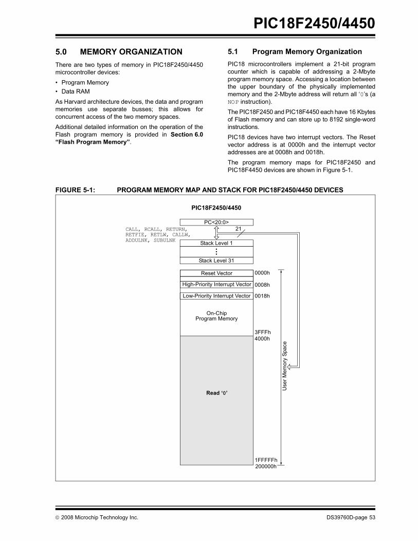
PIC18F2450/4450
© 2008 Microchip Technology Inc. DS39760D-page 53
5.0 MEMORY ORGANIZATIONThere are two types of memory in PIC18F2450/4450microcontroller devices:
� Program Memory� Data RAM
As Harvard architecture devices, the data and programmemories use separate busses; this allows forconcurrent access of the two memory spaces.
Additional detailed information on the operation of theFlash program memory is provided in Section 6.0�Flash Program Memory�.
5.1 Program Memory OrganizationPIC18 microcontrollers implement a 21-bit programcounter which is capable of addressing a 2-Mbyteprogram memory space. Accessing a location betweenthe upper boundary of the physically implementedmemory and the 2-Mbyte address will return all �0�s (aNOP instruction).
The PIC18F2450 and PIC18F4450 each have 16 Kbytesof Flash memory and can store up to 8192 single-wordinstructions.
PIC18 devices have two interrupt vectors. The Resetvector address is at 0000h and the interrupt vectoraddresses are at 0008h and 0018h.
The program memory maps for PIC18F2450 andPIC18F4450 devices are shown in Figure 5-1.
FIGURE 5-1: PROGRAM MEMORY MAP AND STACK FOR PIC18F2450/4450 DEVICES
PC<20:0>
Stack Level 1•
Stack Level 31
Reset Vector
Low-Priority Interrupt Vector
••
CALL, RCALL, RETURN,RETFIE, RETLW, CALLW,
21
0000h
0018h
On-ChipProgram Memory
High-Priority Interrupt Vector 0008hU
ser M
emor
y Sp
ace
1FFFFFh
4000h3FFFh
Read �0�
200000h
PIC18F2450/4450
ADDULNK, SUBULNK

PIC18F2450/4450
DS39760D-page 54 © 2008 Microchip Technology Inc.
5.1.1 PROGRAM COUNTERThe Program Counter (PC) specifies the address of theinstruction to fetch for execution. The PC is 21 bits wideand is contained in three separate 8-bit registers. Thelow byte, known as the PCL register, is both readableand writable. The high byte, or PCH register, containsthe PC<15:8> bits; it is not directly readable or writable.Updates to the PCH register are performed through thePCLATH register. The upper byte is called PCU. Thisregister contains the PC<20:16> bits; it is also notdirectly readable or writable. Updates to the PCUregister are performed through the PCLATU register.
The contents of PCLATH and PCLATU are transferredto the program counter by any operation that writesPCL. Similarly, the upper two bytes of the programcounter are transferred to PCLATH and PCLATU by anoperation that reads PCL. This is useful for computedoffsets to the PC (see Section 5.1.4.1 �ComputedGOTO�).
The PC addresses bytes in the program memory. Toprevent the PC from becoming misaligned with wordinstructions, the Least Significant bit of PCL is fixed toa value of �0�. The PC increments by 2 to addresssequential instructions in the program memory.
The CALL, RCALL and GOTO program branchinstructions write to the program counter directly. Forthese instructions, the contents of PCLATH andPCLATU are not transferred to the program counter.
5.1.2 RETURN ADDRESS STACKThe return address stack allows any combination of upto 31 program calls and interrupts to occur. The PC ispushed onto the stack when a CALL or RCALLinstruction is executed or an interrupt is Acknowledged.The PC value is pulled off the stack on a RETURN,RETLW or a RETFIE instruction. PCLATU and PCLATHare not affected by any of the RETURN or CALLinstructions.
The stack operates as a 31-word by 21-bit RAM and a5-bit Stack Pointer, STKPTR. The stack space is notpart of either program or data space. The Stack Pointeris readable and writable and the address on the top ofthe stack is readable and writable through the Top-of-Stack Special Function Registers. Data can also bepushed to, or popped from the stack, using theseregisters.
A CALL type instruction causes a push onto the stack.The Stack Pointer is first incremented and the locationpointed to by the Stack Pointer is written with thecontents of the PC (already pointing to the instructionfollowing the CALL). A RETURN type instruction causesa pop from the stack. The contents of the locationpointed to by the STKPTR are transferred to the PCand then the Stack Pointer is decremented.
The Stack Pointer is initialized to �00000� after allResets. There is no RAM associated with the locationcorresponding to a Stack Pointer value of �00000�; thisis only a Reset value. Status bits indicate if the stack isfull, has overflowed or has underflowed.
5.1.2.1 Top-of-Stack AccessOnly the top of the return address stack (TOS) isreadable and writable. A set of three registers,TOSU:TOSH:TOSL, hold the contents of the stack loca-tion pointed to by the STKPTR register (Figure 5-2). Thisallows users to implement a software stack if necessary.After a CALL, RCALL or interrupt, the software can readthe pushed value by reading the TOSU:TOSH:TOSLregisters. These values can be placed on a user-definedsoftware stack. At return time, the software can returnthese values to TOSU:TOSH:TOSL and do a return.
The user must disable the global interrupt enable bitswhile accessing the stack to prevent inadvertent stackcorruption.
FIGURE 5-2: RETURN ADDRESS STACK AND ASSOCIATED REGISTERS
00011001A34h
111111111011101
000100000100000
00010
Return Address Stack<20:0>
Top-of-Stack000D58h
TOSLTOSHTOSU34h1Ah00h
STKPTR<4:0>
Top-of-Stack Registers Stack Pointer

PIC18F2450/4450
© 2008 Microchip Technology Inc. DS39760D-page 55
5.1.2.2 Return Stack Pointer (STKPTR)The STKPTR register (Register 5-1) contains the StackPointer value, the STKFUL (Stack Full) status bit andthe STKUNF (Stack Underflow) status bit. The value ofthe Stack Pointer can be 0 through 31. The StackPointer increments before values are pushed onto thestack and decrements after values are popped off thestack. On Reset, the Stack Pointer value will be zero.The user may read and write the Stack Pointer value.This feature can be used by a Real-Time OperatingSystem (RTOS) for return stack maintenance.
After the PC is pushed onto the stack 31 times (withoutpopping any values off the stack), the STKFUL bit isset. The STKFUL bit is cleared by software or by aPOR.
The action that takes place when the stack becomesfull depends on the state of the STVREN (StackOverflow Reset Enable) Configuration bit. (Refer toSection 18.1 �Configuration Bits� for a description ofthe device Configuration bits.) If STVREN is set(default), the 31st push will push the (PC + 2) valueonto the stack, set the STKFUL bit and reset thedevice. The STKFUL bit will remain set and the StackPointer will be set to zero.
If STVREN is cleared, the STKFUL bit will be set on the31st push and the Stack Pointer will increment to 31.Any additional pushes will not overwrite the 31st pushand the STKPTR will remain at 31.
When the stack has been popped enough times tounload the stack, the next pop will return a value of zeroto the PC and sets the STKUNF bit, while the StackPointer remains at zero. The STKUNF bit will remainset until cleared by software or until a POR occurs.
5.1.2.3 PUSH and POP InstructionsSince the Top-of-Stack is readable and writable, theability to push values onto the stack and pull values offthe stack, without disturbing normal program execu-tion, is a desirable feature. The PIC18 instruction setincludes two instructions, PUSH and POP, that permitthe TOS to be manipulated under software control.TOSU, TOSH and TOSL can be modified to place dataor a return address on the stack.
The PUSH instruction places the current PC value ontothe stack. This increments the Stack Pointer and loadsthe current PC value onto the stack.
The POP instruction discards the current TOS bydecrementing the Stack Pointer. The previous valuepushed onto the stack then becomes the TOS value.
Note: Returning a value of zero to the PC on anunderflow has the effect of vectoring theprogram to the Reset vector, where thestack conditions can be verified andappropriate actions can be taken. This isnot the same as a Reset, as the contentsof the SFRs are not affected.
REGISTER 5-1: STKPTR: STACK POINTER REGISTER
R/C-0 R/C-0 U-0 R/W-0 R/W-0 R/W-0 R/W-0 R/W-0STKFUL(1) STKUNF(1) � SP4 SP3 SP2 SP1 SP0
bit 7 bit 0
Legend: C = Clearable bitR = Readable bit W = Writable bit U = Unimplemented bit, read as �0�-n = Value at POR �1� = Bit is set �0� = Bit is cleared x = Bit is unknown
bit 7 STKFUL: Stack Full Flag bit(1)
1 = Stack became full or overflowed 0 = Stack has not become full or overflowed
bit 6 STKUNF: Stack Underflow Flag bit(1)
1 = Stack underflow occurred 0 = Stack underflow did not occur
bit 5 Unimplemented: Read as �0�bit 4-0 SP4:SP0: Stack Pointer Location bits
Note 1: Bit 7 and bit 6 are cleared by user software or by a POR.

PIC18F2450/4450
DS39760D-page 56 © 2008 Microchip Technology Inc.
5.1.2.4 Stack Full and Underflow ResetsDevice Resets on stack overflow and stack underflowconditions are enabled by setting the STVREN bit inConfiguration Register 4L. When STVREN is set, a fullor underflow condition will set the appropriate STKFULor STKUNF bit and then cause a device Reset. WhenSTVREN is cleared, a full or underflow condition will setthe appropriate STKFUL or STKUNF bit but not causea device Reset. The STKFUL or STKUNF bits arecleared by user software or a Power-on Reset.
5.1.3 FAST REGISTER STACKA Fast Register Stack is provided for the STATUS,WREG and BSR registers to provide a �fast return�option for interrupts. Each stack is only one level deepand is neither readable nor writable. It is loaded with thecurrent value of the corresponding register when theprocessor vectors for an interrupt. All interrupt sourceswill push values into the stack registers. The values inthe registers are then loaded back into their associatedregisters if the RETFIE, FAST instruction is used toreturn from the interrupt.
If both low and high-priority interrupts are enabled, thestack registers cannot be used reliably to return fromlow-priority interrupts. If a high-priority interrupt occurswhile servicing a low-priority interrupt, the stackregister values stored by the low-priority interrupt willbe overwritten. In these cases, users must save the keyregisters in software during a low-priority interrupt.
If interrupt priority is not used, all interrupts may use theFast Register Stack for returns from interrupt. If nointerrupts are used, the Fast Register Stack can beused to restore the STATUS, WREG and BSR registersat the end of a subroutine call. To use the Fast RegisterStack for a subroutine call, a CALL label, FASTinstruction must be executed to save the STATUS,WREG and BSR registers to the Fast Register Stack. ARETURN, FAST instruction is then executed to restorethese registers from the Fast Register Stack.
Example 5-1 shows a source code example that usesthe Fast Register Stack during a subroutine call andreturn.
EXAMPLE 5-1: FAST REGISTER STACK CODE EXAMPLE
5.1.4 LOOK-UP TABLES IN PROGRAM MEMORY
There may be programming situations that require thecreation of data structures, or look-up tables, inprogram memory. For PIC18 devices, look-up tablescan be implemented in two ways:
� Computed GOTO � Table Reads
5.1.4.1 Computed GOTOA computed GOTO is accomplished by adding an offsetto the program counter. An example is shown inExample 5-2.
A look-up table can be formed with an ADDWF PCLinstruction and a group of RETLW nn instructions. TheW register is loaded with an offset into the table beforeexecuting a call to that table. The first instruction of thecalled routine is the ADDWF PCL instruction. The nextinstruction executed will be one of the RETLW nninstructions that returns the value �nn� to the callingfunction.
The offset value (in WREG) specifies the number ofbytes that the program counter should advance andshould be multiples of 2 (LSb = 0).
In this method, only one data byte may be stored ineach instruction location and room on the returnaddress stack is required.
EXAMPLE 5-2: COMPUTED GOTO USING AN OFFSET VALUE
5.1.4.2 Table Reads and Table WritesA better method of storing data in program memoryallows two bytes of data to be stored in each instructionlocation.
Look-up table data may be stored two bytes perprogram word by using table reads and writes. TheTable Pointer (TBLPTR) register specifies the byteaddress and the Table Latch (TABLAT) registercontains the data that is read from or written to programmemory. Data is transferred to or from programmemory one byte at a time.
Table read and table write operations are discussedfurther in Section 6.1 �Table Reads and TableWrites�.
CALL SUB1, FAST ;STATUS, WREG, BSR;SAVED IN FAST REGISTER;STACK
• •
SUB1 • •RETURN, FAST ;RESTORE VALUES SAVED
;IN FAST REGISTER STACK
MOVF OFFSET, WCALL TABLE
ORG nn00hTABLE ADDWF PCL
RETLW nnhRETLW nnhRETLW nnh...

PIC18F2450/4450
© 2008 Microchip Technology Inc. DS39760D-page 57
5.2 PIC18 Instruction Cycle
5.2.1 CLOCKING SCHEMEThe microcontroller clock input, whether from aninternal or external source, is internally divided by fourto generate four non-overlapping quadrature clocks(Q1, Q2, Q3 and Q4). Internally, the program counter isincremented on every Q1; the instruction is fetchedfrom the program memory and latched into the Instruc-tion Register (IR) during Q4. The instruction is decodedand executed during the following Q1 through Q4. Theclocks and instruction execution flow are shown inFigure 5-3.
5.2.2 INSTRUCTION FLOW/PIPELININGAn �Instruction Cycle� consists of four Q cycles: Q1through Q4. The instruction fetch and execute arepipelined in such a manner that a fetch takes oneinstruction cycle, while the decode and execute takesanother instruction cycle. However, due to thepipelining, each instruction effectively executes in onecycle. If an instruction causes the program counter tochange (e.g., GOTO), then two cycles are required tocomplete the instruction (Example 5-3).
A fetch cycle begins with the Program Counter (PC)incrementing in Q1.
In the execution cycle, the fetched instruction is latchedinto the Instruction Register (IR) in cycle Q1. Thisinstruction is then decoded and executed during theQ2, Q3 and Q4 cycles. Data memory is read during Q2(operand read) and written during Q4 (destinationwrite).
FIGURE 5-3: CLOCK/INSTRUCTION CYCLE
EXAMPLE 5-3: INSTRUCTION PIPELINE FLOW
Q1 Q2 Q3 Q4 Q1 Q2 Q3 Q4 Q1 Q2 Q3 Q4OSC1
Q1
Q2Q3
Q4
PC
OSC2/CLKO(RC mode)
PC PC + 2 PC + 4
Fetch INST (PC)Execute INST (PC � 2)
Fetch INST (PC + 2)Execute INST (PC)
Fetch INST (PC + 4)Execute INST (PC + 2)
InternalPhaseClock
Note: All instructions are single cycle, except for any program branches. These take two cycles since the fetchinstruction is �flushed� from the pipeline while the new instruction is being fetched and then executed.
TCY0 TCY1 TCY2 TCY3 TCY4 TCY51. MOVLW 55h Fetch 1 Execute 12. MOVWF PORTB Fetch 2 Execute 23. BRA SUB_1 Fetch 3 Execute 34. BSF PORTA, BIT3 (Forced NOP) Fetch 4 Flush (NOP)5. Instruction @ address SUB_1 Fetch SUB_1 Execute SUB_1

PIC18F2450/4450
DS39760D-page 58 © 2008 Microchip Technology Inc.
5.2.3 INSTRUCTIONS IN PROGRAM MEMORY
The program memory is addressed in bytes.Instructions are stored as two bytes or four bytes inprogram memory. The Least Significant Byte of aninstruction word is always stored in a program memorylocation with an even address (LSb = 0). To maintainalignment with instruction boundaries, the PCincrements in steps of 2 and the LSb will always read�0� (see Section 5.1.1 �Program Counter�).
Figure 5-4 shows an example of how instruction wordsare stored in the program memory.
The CALL and GOTO instructions have the absoluteprogram memory address embedded into theinstruction. Since instructions are always stored on wordboundaries, the data contained in the instruction is aword address. The word address is written to PC<20:1>,which accesses the desired byte address in programmemory. Instruction #2 in Figure 5-4 shows how theinstruction, GOTO 0006h, is encoded in the programmemory. Program branch instructions, which encode arelative address offset, operate in the same manner. Theoffset value stored in a branch instruction represents thenumber of single-word instructions that the PC will beoffset by. Section 19.0 �Instruction Set Summary�provides further details of the instruction set.
FIGURE 5-4: INSTRUCTIONS IN PROGRAM MEMORY
5.2.4 TWO-WORD INSTRUCTIONSThe standard PIC18 instruction set has four two-wordinstructions: CALL, MOVFF, GOTO and LSFR. In allcases, the second word of the instructions always has�1111� as its four Most Significant bits; the other 12 bitsare literal data, usually a data memory address.
The use of �1111� in the 4 MSbs of an instructionspecifies a special form of NOP. If the instruction isexecuted in proper sequence, immediately after thefirst word, the data in the second word is accessed and
used by the instruction sequence. If the first word isskipped for some reason and the second word isexecuted by itself, a NOP is executed instead. This isnecessary for cases when the two-word instruction ispreceded by a conditional instruction that changes thePC. Example 5-4 shows how this works.
EXAMPLE 5-4: TWO-WORD INSTRUCTIONS
Word AddressLSB = 1 LSB = 0 ↓
Program MemoryByte Locations →
000000h000002h000004h000006h
Instruction 1: MOVLW 055h 0Fh 55h 000008hInstruction 2: GOTO 0006h EFh 03h 00000Ah
F0h 00h 00000ChInstruction 3: MOVFF 123h, 456h C1h 23h 00000Eh
F4h 56h 000010h000012h000014h
Note: See Section 5.5 �Program Memory andthe Extended Instruction Set� forinformation on two-word instruction in theextended instruction set.
CASE 1:Object Code Source Code0110 0110 0000 0000 TSTFSZ REG1 ; is RAM location 0?
1100 0001 0010 0011 MOVFF REG1, REG2 ; No, skip this word
1111 0100 0101 0110 ; Execute this word as a NOP
0010 0100 0000 0000 ADDWF REG3 ; continue code
CASE 2:Object Code Source Code0110 0110 0000 0000 TSTFSZ REG1 ; is RAM location 0?
1100 0001 0010 0011 MOVFF REG1, REG2 ; Yes, execute this word
1111 0100 0101 0110 ; 2nd word of instruction
0010 0100 0000 0000 ADDWF REG3 ; continue code
PIC18F2450/4450
© 2008 Microchip Technology Inc. DS39760D-page 59
5.3 Data Memory Organization
The data memory in PIC18 devices is implemented asstatic RAM. Each register in the data memory has a12-bit address, allowing up to 4096 bytes of datamemory. The memory space is divided into as many as16 banks that contain 256 bytes each. PIC18F2450/4450 devices implement three complete banks, for atotal of 768 bytes. Figure 5-5 shows the data memoryorganization for the devices.
The data memory contains Special Function Registers(SFRs) and General Purpose Registers (GPRs). TheSFRs are used for control and status of the controllerand peripheral functions, while GPRs are used for datastorage and scratchpad operations in the user�sapplication. Any read of an unimplemented location willread as �0�s.
The instruction set and architecture allow operationsacross all banks. The entire data memory may beaccessed by Direct, Indirect or Indexed Addressingmodes. Addressing modes are discussed later in thissubsection.
To ensure that commonly used registers (SFRs andselect GPRs) can be accessed in a single cycle, PIC18devices implement an Access Bank. This is a 256-bytememory space that provides fast access to SFRs andthe lower portion of GPR Bank 0 without using theBSR. Section 5.3.3 �Access Bank� provides adetailed description of the Access RAM.
5.3.1 USB RAMBank 4 of the data memory is actually mapped tospecial dual port RAM. When the USB module isdisabled, the GPRs in these banks are used like anyother GPR in the data memory space.
When the USB module is enabled, the memory in thisbank is allocated as buffer RAM for USB operation.This area is shared between the microcontroller coreand the USB Serial Interface Engine (SIE) and is usedto transfer data directly between the two.
It is theoretically possible to use this area of USB RAMthat is not allocated as USB buffers for normal scratch-pad memory or other variable storage. In practice, thedynamic nature of buffer allocation makes this risky atbest. Bank 4 is also used for USB buffer managementwhen the module is enabled and should not be used forany other purposes during that time.
Additional information on USB RAM and bufferoperation is provided in Section 14.0 �UniversalSerial Bus (USB)�.
5.3.2 BANK SELECT REGISTER (BSR)Large areas of data memory require an efficientaddressing scheme to make rapid access to anyaddress possible. Ideally, this means that an entireaddress does not need to be provided for each read orwrite operation. For PIC18 devices, this isaccomplished with a RAM banking scheme. Thisdivides the memory space into 16 contiguous banks of256 bytes. Depending on the instruction, each locationcan be addressed directly by its full 12-bit address, oran 8-bit low-order address and a 4-bit Bank Pointer.
Most instructions in the PIC18 instruction set make useof the Bank Pointer, known as the Bank Select Register(BSR). This SFR holds the 4 Most Significant bits of alocation�s address; the instruction itself includes the8 Least Significant bits. Only the four lower bits of theBSR are implemented (BSR3:BSR0). The upper fourbits are unused; they will always read �0� and cannot bewritten to. The BSR can be loaded directly by using theMOVLB instruction.
The value of the BSR indicates the bank in datamemory. The eight bits in the instruction show the loca-tion in the bank and can be thought of as an offset fromthe bank�s lower boundary. The relationship betweenthe BSR�s value and the bank division in data memoryis shown in Figure 5-6.
Since up to 16 registers may share the same low-orderaddress, the user must always be careful to ensure thatthe proper bank is selected before performing a dataread or write. For example, writing what should beprogram data to an 8-bit address of F9h, while the BSRis 0Fh, will end up resetting the program counter.
While any bank can be selected, only those banks thatare actually implemented can be read or written to.Writes to unimplemented banks are ignored, whilereads from unimplemented banks will return �0�s. Evenso, the STATUS register will still be affected as if theoperation was successful. The data memory map inFigure 5-6 indicates which banks are implemented.
In the core PIC18 instruction set, only the MOVFFinstruction fully specifies the 12-bit address of thesource and target registers. This instruction ignores theBSR completely when it executes. All other instructionsinclude only the low-order address as an operand andmust use either the BSR or the Access Bank to locatetheir target registers.
Note: The operation of some aspects of datamemory are changed when the PIC18extended instruction set is enabled. SeeSection 5.6 �Data Memory and theExtended Instruction Set� for moreinformation.
PIC18F2450/4450
DS39760D-page 60 © 2008 Microchip Technology Inc.
FIGURE 5-5: DATA MEMORY MAP FOR PIC18F2450/4450 DEVICES
Bank 0
Bank 1
Bank 14
Bank 15
Data Memory MapBSR<3:0>
= 0000
= 0001
= 1111
060h05Fh
F60hFFFh
00h5Fh60h
FFh
Access Bank
When a = 0: The BSR is ignored and theAccess Bank is used.The first 96 bytes are general purpose RAM (from Bank 0). The remaining 160 bytes areSpecial Function Registers(from Bank 15).
When a = 1: The BSR specifies the bankused by the instruction.
F5FhF00hEFFh
1FFh
100h0FFh
000hAccess RAM
FFh
00h
FFh
00h
FFh
00h
GPR
GPR
SFR
Access RAM High
Access RAM Low
Bank 2= 0010
(SFRs)
2FFh
200h
3FFh
300h
4FFh
400h
800h
Bank 3
Bank 4
Bank 5
FFh
00h
FFh
00h
FFh
00h
00h
Unused
Unused
FFh
= 0011
= 0100
= 0101
UnusedRead as 00h
to
= 1110
Note 1: This bank also serve as RAM buffer for USB operation. See Section 5.3.1 �USB RAM� for more information.
Unused
GPR(1)
Read as 00h
Read as 00h

PIC18F2450/4450
© 2008 Microchip Technology Inc. DS39760D-page 61
FIGURE 5-6: USE OF THE BANK SELECT REGISTER (DIRECT ADDRESSING)
5.3.3 ACCESS BANKWhile the use of the BSR, with an embedded 8-bitaddress, allows users to address the entire range ofdata memory, it also means that the user must alwaysensure that the correct bank is selected. Otherwise,data may be read from or written to the wrong location.This can be disastrous if a GPR is the intended targetof an operation but an SFR is written to instead.Verifying and/or changing the BSR for each read orwrite to data memory can become very inefficient.
To streamline access for the most commonly used datamemory locations, the data memory is configured withan Access Bank, which allows users to access amapped block of memory without specifying a BSR.The Access Bank consists of the first 96 bytes ofmemory (00h-5Fh) in Bank 0 and the last 160 bytes ofmemory (60h-FFh) in Block 15. The lower half is knownas the �Access RAM� and is composed of GPRs. Theupper half is where the device�s SFRs are mapped.These two areas are mapped contiguously in theAccess Bank and can be addressed in a linear fashionby an 8-bit address (Figure 5-5).
The Access Bank is used by core PIC18 instructionsthat include the Access RAM bit (the �a� parameter inthe instruction). When �a� is equal to �1�, the instructionuses the BSR and the 8-bit address included in theopcode for the data memory address. When �a� is �0�,
however, the instruction is forced to use the AccessBank address map; the current value of the BSR isignored entirely.
Using this �forced� addressing allows the instruction tooperate on a data address in a single cycle withoutupdating the BSR first. For 8-bit addresses of 60h andabove, this means that users can evaluate and operateon SFRs more efficiently. The Access RAM below 60his a good place for data values that the user might needto access rapidly, such as immediate computationalresults or common program variables. Access RAMalso allows for faster and more code efficient contextsaving and switching of variables.
The mapping of the Access Bank is slightly differentwhen the extended instruction set is enabled (XINSTConfiguration bit = 1). This is discussed in more detailin Section 5.6.3 �Mapping the Access Bank inIndexed Literal Offset Mode�.
5.3.4 GENERAL PURPOSE REGISTER FILE
PIC18 devices may have banked memory in the GPRarea. This is data RAM which is available for use by allinstructions. GPRs start at the bottom of Bank 0(address 000h) and grow upwards towards the bottom ofthe SFR area. GPRs are not initialized by a Power-onReset and are unchanged on all other Resets.
Note 1: The Access RAM bit of the instruction can be used to force an override of the selected bank (BSR<3:0>) to the registers of the Access Bank.
2: The MOVFF instruction embeds the entire 12-bit address in the instruction.
Data Memory
Bank Select(2)
7 0From Opcode(2)
0 0 0 0
000h
100h
200h
300h
F00h
E00h
FFFh
Bank 0
Bank 1
Bank 2
Bank 14
Bank 15
00h
FFh00h
FFh00h
FFh
00h
FFh00h
FFh
00h
FFh
Bank 3throughBank 13
0 0 1 1 1 1 1 1 1 1 1 1
7 0BSR(1)

PIC18F2450/4450
DS39760D-page 62 © 2008 Microchip Technology Inc.
5.3.5 SPECIAL FUNCTION REGISTERS
The Special Function Registers (SFRs) are registersused by the CPU and peripheral modules for controllingthe desired operation of the device. These registers areimplemented as static RAM in the data memory space.SFRs start at the top of data memory and extenddownward to occupy the top segment of Bank 15, fromF60h to FFFh. A list of these registers is given inTable 5-1 and Table 5-2.
The SFRs can be classified into two sets: thoseassociated with the �core� device functionality (ALU,Resets and interrupts) and those related to the
peripheral functions. The Reset and interrupt registersare described in their respective chapters, while theALU�s STATUS register is described later in thissection. Registers related to the operation of aperipheral feature are described in the chapter for thatperipheral.
The SFRs are typically distributed among theperipherals whose functions they control. Unused SFRlocations are unimplemented and read as �0�s.
TABLE 5-1: SPECIAL FUNCTION REGISTER MAP FOR PIC18F2450/4450 DEVICES
Address Name Address Name Address Name Address Name Address Name
FFFh TOSU FDFh INDF2(1) FBFh CCPR1H F9Fh IPR1 F7Fh UEP15FFEh TOSH FDEh POSTINC2(1) FBEh CCPR1L F9Eh PIR1 F7Eh UEP14FFDh TOSL FDDh POSTDEC2(1) FBDh CCP1CON F9Dh PIE1 F7Dh UEP13FFCh STKPTR FDCh PREINC2(1) FBCh �(2) F9Ch �(2) F7Ch UEP12FFBh PCLATU FDBh PLUSW2(1) FBBh �(2) F9Bh �(2) F7Bh UEP11FFAh PCLATH FDAh FSR2H FBAh �(2) F9Ah �(2) F7Ah UEP10FF9h PCL FD9h FSR2L FB9h �(2) F99h �(2) F79h UEP9FF8h TBLPTRU FD8h STATUS FB8h BAUDCON F98h �(2) F78h UEP8FF7h TBLPTRH FD7h TMR0H FB7h �(2) F97h �(2) F77h UEP7FF6h TBLPTRL FD6h TMR0L FB6h �(2) F96h TRISE(3) F76h UEP6FF5h TABLAT FD5h T0CON FB5h �(2) F95h TRISD(3) F75h UEP5FF4h PRODH FD4h �(2) FB4h �(2) F94h TRISC F74h UEP4FF3h PRODL FD3h OSCCON FB3h �(2) F93h TRISB F73h UEP3FF2h INTCON FD2h HLVDCON FB2h �(2) F92h TRISA F72h UEP2FF1h INTCON2 FD1h WDTCON FB1h �(2) F91h �(2) F71h UEP1FF0h INTCON3 FD0h RCON FB0h SPBRGH F90h �(2) F70h UEP0FEFh INDF0(1) FCFh TMR1H FAFh SPBRG F8Fh �(2) F6Fh UCFGFEEh POSTINC0(1) FCEh TMR1L FAEh RCREG F8Eh �(2) F6Eh UADDRFEDh POSTDEC0(1) FCDh T1CON FADh TXREG F8Dh LATE(3) F6Dh UCONFECh PREINC0(1) FCCh TMR2 FACh TXSTA F8Ch LATD(3) F6Ch USTATFEBh PLUSW0(1) FCBh PR2 FABh RCSTA F8Bh LATC F6Bh UEIEFEAh FSR0H FCAh T2CON FAAh �(2) F8Ah LATB F6Ah UEIRFE9h FSR0L FC9h �(2) FA9h �(2) F89h LATA F69h UIEFE8h WREG FC8h �(2) FA8h �(2) F88h �(2) F68h UIRFE7h INDF1(1) FC7h �(2) FA7h EECON2(1) F87h �(2) F67h UFRMHFE6h POSTINC1(1) FC6h �(2) FA6h EECON1 F86h �(2) F66h UFRMLFE5h POSTDEC1(1) FC5h �(2) FA5h �(2) F85h �(2) F65h �(2)
FE4h PREINC1(1) FC4h ADRESH FA4h �(2) F84h PORTE F64h �(2)
FE3h PLUSW1(1) FC3h ADRESL FA3h �(2) F83h PORTD(3) F63h �(2)
FE2h FSR1H FC2h ADCON0 FA2h IPR2 F82h PORTC F62h �(2)
FE1h FSR1L FC1h ADCON1 FA1h PIR2 F81h PORTB F61h �(2)
FE0h BSR FC0h ADCON2 FA0h PIE2 F80h PORTA F60h �(2)
Note 1: Not a physical register.2: Unimplemented registers are read as �0�.3: These registers are implemented only on 40/44-pin devices.
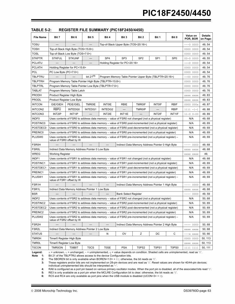
PIC18F2450/4450
© 2008 Microchip Technology Inc. DS39760D-page 63
TABLE 5-2: REGISTER FILE SUMMARY (PIC18F2450/4450)
File Name Bit 7 Bit 6 Bit 5 Bit 4 Bit 3 Bit 2 Bit 1 Bit 0 Value on POR, BOR
Details on Page:
TOSU � � � Top-of-Stack Upper Byte (TOS<20:16>) ---0 0000 49, 54
TOSH Top-of-Stack High Byte (TOS<15:8>) 0000 0000 49, 54
TOSL Top-of-Stack Low Byte (TOS<7:0>) 0000 0000 49, 54
STKPTR STKFUL STKUNF � SP4 SP3 SP2 SP1 SP0 00-0 0000 49, 55
PCLATU � � � Holding Register for PC<20:16> ---0 0000 49, 54
PCLATH Holding Register for PC<15:8> 0000 0000 49, 54
PCL PC Low Byte (PC<7:0>) 0000 0000 49, 54
TBLPTRU � � bit 21(1) Program Memory Table Pointer Upper Byte (TBLPTR<20:16>) --00 0000 49, 76
TBLPTRH Program Memory Table Pointer High Byte (TBLPTR<15:8>) 0000 0000 49, 76
TBLPTRL Program Memory Table Pointer Low Byte (TBLPTR<7:0>) 0000 0000 49, 76
TABLAT Program Memory Table Latch 0000 0000 49, 76
PRODH Product Register High Byte xxxx xxxx 49, 83
PRODL Product Register Low Byte xxxx xxxx 49, 83
INTCON GIE/GIEH PEIE/GIEL TMR0IE INT0IE RBIE TMR0IF INT0IF RBIF 0000 000x 49, 87
INTCON2 RBPU INTEDG0 INTEDG1 INTEDG2 � TMR0IP � RBIP 1111 -1-1 49, 88
INTCON3 INT2IP INT1IP � INT2IE INT1IE � INT2IF INT1IF 11-0 0-00 49, 89
INDF0 Uses contents of FSR0 to address data memory � value of FSR0 not changed (not a physical register) N/A 49, 68
POSTINC0 Uses contents of FSR0 to address data memory � value of FSR0 post-incremented (not a physical register) N/A 49, 69
POSTDEC0 Uses contents of FSR0 to address data memory � value of FSR0 post-decremented (not a physical register) N/A 49, 69
PREINC0 Uses contents of FSR0 to address data memory � value of FSR0 pre-incremented (not a physical register) N/A 49, 69
PLUSW0 Uses contents of FSR0 to address data memory � value of FSR0 pre-incremented (not a physical register) � value of FSR0 offset by W
N/A 49, 69
FSR0H � � � � Indirect Data Memory Address Pointer 0 High Byte ---- 0000 49, 68
FSR0L Indirect Data Memory Address Pointer 0 Low Byte xxxx xxxx 49, 68
WREG Working Register xxxx xxxx 49,
INDF1 Uses contents of FSR1 to address data memory � value of FSR1 not changed (not a physical register) N/A 49, 68
POSTINC1 Uses contents of FSR1 to address data memory � value of FSR1 post-incremented (not a physical register) N/A 49, 69
POSTDEC1 Uses contents of FSR1 to address data memory � value of FSR1 post-decremented (not a physical register) N/A 49, 69
PREINC1 Uses contents of FSR1 to address data memory � value of FSR1 pre-incremented (not a physical register) N/A 49, 69
PLUSW1 Uses contents of FSR1 to address data memory � value of FSR1 pre-incremented (not a physical register) � value of FSR1 offset by W
N/A 49, 69
FSR1H � � � � Indirect Data Memory Address Pointer 1 High Byte ---- 0000 49, 68
FSR1L Indirect Data Memory Address Pointer 1 Low Byte xxxx xxxx 49, 68
BSR � � � � Bank Select Register ---- 0000 49, 59
INDF2 Uses contents of FSR2 to address data memory � value of FSR2 not changed (not a physical register) N/A 50, 68
POSTINC2 Uses contents of FSR2 to address data memory � value of FSR2 post-incremented (not a physical register) N/A 50, 69
POSTDEC2 Uses contents of FSR2 to address data memory � value of FSR2 post-decremented (not a physical register) N/A 50, 69
PREINC2 Uses contents of FSR2 to address data memory � value of FSR2 pre-incremented (not a physical register) N/A 50, 69
PLUSW2 Uses contents of FSR2 to address data memory � value of FSR2 pre-incremented (not a physical register) � value of FSR2 offset by W
N/A 50, 69
FSR2H � � � � Indirect Data Memory Address Pointer 2 High Byte ---- 0000 50, 68
FSR2L Indirect Data Memory Address Pointer 2 Low Byte xxxx xxxx 50, 68
STATUS � � � N OV Z DC C ---x xxxx 50, 66
TMR0H Timer0 Register High Byte 0000 0000 50, 113
TMR0L Timer0 Register Low Byte xxxx xxxx 50, 113
T0CON TMR0ON T08BIT T0CS T0SE PSA T0PS2 T0PS1 T0PS0 1111 1111 50, 111
Legend: x = unknown, u = unchanged, - = unimplemented, q = value depends on condition. Shaded cells are unimplemented, read as �0�.Note 1: Bit 21 of the TBLPTRU allows access to the device Configuration bits.
2: The SBOREN bit is only available when BOREN<1:0> = 01; otherwise, the bit reads as �0�.3: These registers and/or bits are not implemented on 28-pin devices and are read as �0�. Reset values are shown for 40/44-pin devices;
individual unimplemented bits should be interpreted as �-�.4: RA6 is configured as a port pin based on various primary oscillator modes. When the port pin is disabled, all of the associated bits read �0�.5: RE3 is only available as a port pin when the MCLRE Configuration bit is clear; otherwise, the bit reads as �0�.6: RC5 and RC4 are only available as port pins when the USB module is disabled (UCON<3> = 0).

PIC18F2450/4450
DS39760D-page 64 © 2008 Microchip Technology Inc.
OSCCON IDLEN � � � OSTS � SCS1 SCS0 0--- q-00 50, 31
HLVDCON VDIRMAG � IRVST HLVDEN HLVDL3 HLVDL2 HLVDL1 HLVDL0 0-00 0101 50, 185
WDTCON � � � � � � � SWDTEN --- ---0 50, 204
RCON IPEN SBOREN(2) � RI TO PD POR BOR 0q-1 11q0 50, 42
TMR1H Timer1 Register High Byte xxxx xxxx 50, 120
TMR1L Timer1 Register Low Byte xxxx xxxx 50, 120
T1CON RD16 T1RUN T1CKPS1 T1CKPS0 T1OSCEN T1SYNC TMR1CS TMR1ON 0000 0000 50, 115
TMR2 Timer2 Register 0000 0000 50, 122
PR2 Timer2 Period Register 1111 1111 50, 122
T2CON � T2OUTPS3 T2OUTPS2 T2OUTPS1 T2OUTPS0 TMR2ON T2CKPS1 T2CKPS0 -000 0000 50, 121
ADRESH A/D Result Register High Byte xxxx xxxx 50, 184
ADRESL A/D Result Register Low Byte xxxx xxxx 50, 184
ADCON0 � � CHS3 CHS2 CHS1 CHS0 GO/DONE ADON --00 0000 50, 175
ADCON1 � � VCFG1 VCFG0 PCFG3 PCFG2 PCFG1 PCFG0 --00 qqqq 50, 176
ADCON2 ADFM � ACQT2 ACQT1 ACQT0 ADCS2 ADCS1 ADCS0 0-00 0000 50, 177
CCPR1H Capture/Compare/PWM Register 1 High Byte xxxx xxxx 50, 124
CCPR1L Capture/Compare/PWM Register 1 Low Byte xxxx xxxx 50, 124
CCP1CON � � DC1B1 DC1B0 CCP1M3 CCP1M2 CCP1M1 CCP1M0 --00 0000 50, 123,
BAUDCON ABDOVF RCIDL � SCKP BRG16 � WUE ABDEN 01-0 0-00 51, 156,
SPBRGH EUSART Baud Rate Generator Register High Byte 0000 0000 50, 157
SPBRG EUSART Baud Rate Generator Register Low Byte 0000 0000 50, 157
RCREG EUSART Receive Register 0000 0000 50, 165
TXREG EUSART Transmit Register 0000 0000 51, 163
TXSTA CSRC TX9 TXEN SYNC SENDB BRGH TRMT TX9D 0000 0010 51, 154
RCSTA SPEN RX9 SREN CREN ADDEN FERR OERR RX9D 0000 000x 51, 155
EECON2 Data Memory Control Register 2 (not a physical register) 0000 0000 51, 74
EECON1 � CFGS � FREE WRERR WREN WR � -x-0 x00- 51, 75
IPR2 OSCFIP � USBIP � � HLVDIP � � 1-1- -1-- 51, 95
PIR2 OSCFIF � USBIF � � HLVDIF � � 0-0- -0-- 51, 91
PIE2 OSCFIE � USBIE � � HLVDIE � � 0-0- -0-- 51, 93
IPR1 � ADIP RCIP TXIP � CCP1IP TMR2IP TMR1IP -111 -111 51, 94
PIR1 � ADIF RCIF TXIF � CCP1IF TMR2IF TMR1IF -000 -000 51, 90
PIE1 � ADIE RCIE TXIE � CCP1IE TMR2IE TMR1IE -000 -000 51, 92
TRISE(3) � � � � � TRISE2 TRISE1 TRISE0 ---- -111 51, 110
TRISD(3) TRISD7 TRISD6 TRISD5 TRISD4 TRISD3 TRISD2 TRISD1 TRISD0 1111 1111 51, 108
TRISC TRISC7 TRISC6 � � � TRISC2 TRISC1 TRISC0 11-- -111 51, 106
TRISB TRISB7 TRISB6 TRISB5 TRISB4 TRISB3 TRISB2 TRISB1 TRISB0 1111 1111 51, 103
TRISA � TRISA6(4) TRISA5 TRISA4 TRISA3 TRISA2 TRISA1 TRISA0 -111 1111 51, 100
LATE(3) � � � � � LATE2 LATE1 LATE0 ---- -xxx 51, 110
LATD(3) LATD7 LATD6 LATD5 LATD4 LATD3 LATD2 LATD1 LATD0 xxxx xxxx 51, 108
LATC LATC7 LATC6 � � � LATC2 LATC1 LATC0 xx-- -xxx 51, 106
LATB LATB7 LATB6 LATB5 LATB4 LATB3 LATB2 LATB1 LATB0 xxxx xxxx 51, 103
LATA � LATA6(4) LATA5 LATA4 LATA3 LATA2 LATA1 LATA0 -xxx xxxx 51, 100
PORTE � � � � RE3(5) RE2(3) RE1(3) RE0(3) ---- x000 51, 109
PORTD(3) RD7 RD6 RD5 RD4 RD3 RD2 RD1 RD0 xxxx xxxx 51, 108
TABLE 5-2: REGISTER FILE SUMMARY (PIC18F2450/4450) (CONTINUED)
File Name Bit 7 Bit 6 Bit 5 Bit 4 Bit 3 Bit 2 Bit 1 Bit 0 Value on POR, BOR
Details on Page:
Legend: x = unknown, u = unchanged, - = unimplemented, q = value depends on condition. Shaded cells are unimplemented, read as �0�.Note 1: Bit 21 of the TBLPTRU allows access to the device Configuration bits.
2: The SBOREN bit is only available when BOREN<1:0> = 01; otherwise, the bit reads as �0�.3: These registers and/or bits are not implemented on 28-pin devices and are read as �0�. Reset values are shown for 40/44-pin devices;
individual unimplemented bits should be interpreted as �-�.4: RA6 is configured as a port pin based on various primary oscillator modes. When the port pin is disabled, all of the associated bits read �0�.5: RE3 is only available as a port pin when the MCLRE Configuration bit is clear; otherwise, the bit reads as �0�.6: RC5 and RC4 are only available as port pins when the USB module is disabled (UCON<3> = 0).
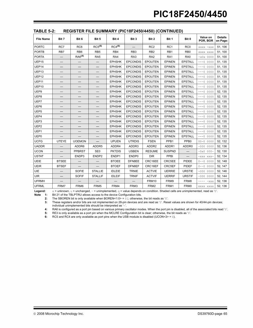
PIC18F2450/4450
© 2008 Microchip Technology Inc. DS39760D-page 65
PORTC RC7 RC6 RC5(6) RC4(6) � RC2 RC1 RC0 xxxx -xxx 51, 106
PORTB RB7 RB6 RB5 RB4 RB3 RB2 RB1 RB0 xxxx xxxx 51, 100
PORTA � RA6(4) RA5 RA4 RA3 RA2 RA1 RA0 -x0x 0000 51, 100
UEP15 � � � EPHSHK EPCONDIS EPOUTEN EPINEN EPSTALL ---0 0000 51, 135
UEP14 � � � EPHSHK EPCONDIS EPOUTEN EPINEN EPSTALL ---0 0000 51, 135
UEP13 � � � EPHSHK EPCONDIS EPOUTEN EPINEN EPSTALL ---0 0000 51, 135
UEP12 � � � EPHSHK EPCONDIS EPOUTEN EPINEN EPSTALL ---0 0000 51, 135
UEP11 � � � EPHSHK EPCONDIS EPOUTEN EPINEN EPSTALL ---0 0000 51, 135
UEP10 � � � EPHSHK EPCONDIS EPOUTEN EPINEN EPSTALL ---0 0000 51, 135
UEP9 � � � EPHSHK EPCONDIS EPOUTEN EPINEN EPSTALL ---0 0000 52, 135
UEP8 � � � EPHSHK EPCONDIS EPOUTEN EPINEN EPSTALL ---0 0000 52, 135
UEP7 � � � EPHSHK EPCONDIS EPOUTEN EPINEN EPSTALL ---0 0000 52, 135
UEP6 � � � EPHSHK EPCONDIS EPOUTEN EPINEN EPSTALL ---0 0000 52, 135
UEP5 � � � EPHSHK EPCONDIS EPOUTEN EPINEN EPSTALL ---0 0000 52, 135
UEP4 � � � EPHSHK EPCONDIS EPOUTEN EPINEN EPSTALL ---0 0000 52, 135
UEP3 � � � EPHSHK EPCONDIS EPOUTEN EPINEN EPSTALL ---0 0000 52, 135
UEP2 � � � EPHSHK EPCONDIS EPOUTEN EPINEN EPSTALL ---0 0000 52, 135
UEP1 � � � EPHSHK EPCONDIS EPOUTEN EPINEN EPSTALL ---0 0000 52, 135
UEP0 � � � EPHSHK EPCONDIS EPOUTEN EPINEN EPSTALL ---0 0000 52, 135
UCFG UTEYE UOEMON � UPUEN UTRDIS FSEN PPB1 PPB0 00-0 0000 52, 132
UADDR � ADDR6 ADDR5 ADDR4 ADDR3 ADDR2 ADDR1 ADDR0 -000 0000 52, 136
UCON � PPBRST SE0 PKTDIS USBEN RESUME SUSPND � -0x0 000- 52, 130
USTAT � ENDP3 ENDP2 ENDP1 ENDP0 DIR PPBI � -xxx xxx- 52, 134
UEIE BTSEE � � BTOEE DFN8EE CRC16EE CRC5EE PIDEE 0--0 0000 52, 148
UEIR BTSEF � � BTOEF DFN8EF CRC16EF CRC5EF PIDEF 0--0 0000 52, 147
UIE � SOFIE STALLIE IDLEIE TRNIE ACTVIE UERRIE URSTIE -000 0000 52, 146
UIR � SOFIF STALLIF IDLEIF TRNIF ACTVIF UERRIF URSTIF -000 0000 52, 144
UFRMH � � � � � FRM10 FRM9 FRM8 ---- -xxx 52, 136
UFRML FRM7 FRM6 FRM5 FRM4 FRM3 FRM2 FRM1 FRM0 xxxx xxxx 52, 136
TABLE 5-2: REGISTER FILE SUMMARY (PIC18F2450/4450) (CONTINUED)
File Name Bit 7 Bit 6 Bit 5 Bit 4 Bit 3 Bit 2 Bit 1 Bit 0 Value on POR, BOR
Details on Page:
Legend: x = unknown, u = unchanged, - = unimplemented, q = value depends on condition. Shaded cells are unimplemented, read as �0�.Note 1: Bit 21 of the TBLPTRU allows access to the device Configuration bits.
2: The SBOREN bit is only available when BOREN<1:0> = 01; otherwise, the bit reads as �0�.3: These registers and/or bits are not implemented on 28-pin devices and are read as �0�. Reset values are shown for 40/44-pin devices;
individual unimplemented bits should be interpreted as �-�.4: RA6 is configured as a port pin based on various primary oscillator modes. When the port pin is disabled, all of the associated bits read �0�.5: RE3 is only available as a port pin when the MCLRE Configuration bit is clear; otherwise, the bit reads as �0�.6: RC5 and RC4 are only available as port pins when the USB module is disabled (UCON<3> = 0).
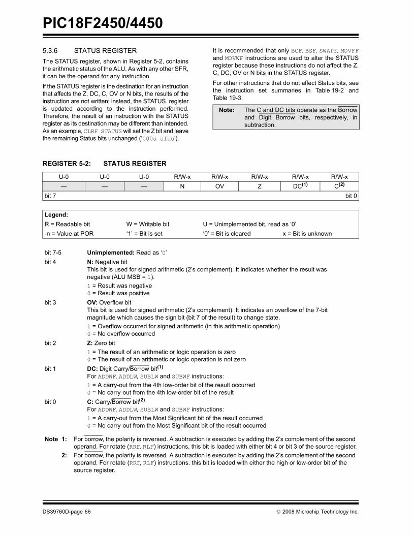
PIC18F2450/4450
DS39760D-page 66 © 2008 Microchip Technology Inc.
5.3.6 STATUS REGISTERThe STATUS register, shown in Register 5-2, containsthe arithmetic status of the ALU. As with any other SFR,it can be the operand for any instruction.
If the STATUS register is the destination for an instructionthat affects the Z, DC, C, OV or N bits, the results of theinstruction are not written; instead, the STATUS registeris updated according to the instruction performed.Therefore, the result of an instruction with the STATUSregister as its destination may be different than intended.As an example, CLRF STATUS will set the Z bit and leavethe remaining Status bits unchanged (�000u u1uu�).
It is recommended that only BCF, BSF, SWAPF, MOVFFand MOVWF instructions are used to alter the STATUSregister because these instructions do not affect the Z,C, DC, OV or N bits in the STATUS register.
For other instructions that do not affect Status bits, seethe instruction set summaries in Table 19-2 andTable 19-3.
Note: The C and DC bits operate as the Borrowand Digit Borrow bits, respectively, insubtraction.
REGISTER 5-2: STATUS REGISTER
U-0 U-0 U-0 R/W-x R/W-x R/W-x R/W-x R/W-x� � � N OV Z DC(1) C(2)
bit 7 bit 0
Legend:R = Readable bit W = Writable bit U = Unimplemented bit, read as �0�-n = Value at POR �1� = Bit is set �0� = Bit is cleared x = Bit is unknown
bit 7-5 Unimplemented: Read as �0�bit 4 N: Negative bit
This bit is used for signed arithmetic (2�s complement). It indicates whether the result was negative (ALU MSB = 1).1 = Result was negative 0 = Result was positive
bit 3 OV: Overflow bit This bit is used for signed arithmetic (2�s complement). It indicates an overflow of the 7-bit magnitude which causes the sign bit (bit 7 of the result) to change state.1 = Overflow occurred for signed arithmetic (in this arithmetic operation) 0 = No overflow occurred
bit 2 Z: Zero bit 1 = The result of an arithmetic or logic operation is zero 0 = The result of an arithmetic or logic operation is not zero
bit 1 DC: Digit Carry/Borrow bit(1) For ADDWF, ADDLW, SUBLW and SUBWF instructions: 1 = A carry-out from the 4th low-order bit of the result occurred 0 = No carry-out from the 4th low-order bit of the result
bit 0 C: Carry/Borrow bit(2) For ADDWF, ADDLW, SUBLW and SUBWF instructions: 1 = A carry-out from the Most Significant bit of the result occurred 0 = No carry-out from the Most Significant bit of the result occurred
Note 1: For borrow, the polarity is reversed. A subtraction is executed by adding the 2�s complement of the second operand. For rotate (RRF, RLF) instructions, this bit is loaded with either bit 4 or bit 3 of the source register.
2: For borrow, the polarity is reversed. A subtraction is executed by adding the 2�s complement of the second operand. For rotate (RRF, RLF) instructions, this bit is loaded with either the high or low-order bit of the source register.
PIC18F2450/4450
© 2008 Microchip Technology Inc. DS39760D-page 67
5.4 Data Addressing Modes
While the program memory can be addressed in onlyone way � through the program counter � informationin the data memory space can be addressed in severalways. For most instructions, the addressing mode isfixed. Other instructions may use up to three modes,depending on which operands are used and whether ornot the extended instruction set is enabled.
The addressing modes are:
� Inherent� Literal� Direct� Indirect
An additional addressing mode, Indexed Literal Offset,is available when the extended instruction set isenabled (XINST Configuration bit = 1). Its operation isdiscussed in greater detail in Section 5.6.1 �IndexedAddressing with Literal Offset�.
5.4.1 INHERENT AND LITERAL ADDRESSING
Many PIC18 control instructions do not need anyargument at all; they either perform an operation thatglobally affects the device or they operate implicitly onone register. This addressing mode is known asInherent Addressing. Examples include SLEEP, RESETand DAW.
Other instructions work in a similar way but require anadditional explicit argument in the opcode. This isknown as Literal Addressing mode because theyrequire some literal value as an argument. Examplesinclude ADDLW and MOVLW, which respectively, add ormove a literal value to the W register. Other examplesinclude CALL and GOTO, which include a 20-bitprogram memory address.
5.4.2 DIRECT ADDRESSINGDirect Addressing mode specifies all or part of thesource and/or destination address of the operationwithin the opcode itself. The options are specified bythe arguments accompanying the instruction.
In the core PIC18 instruction set, bit-oriented and byte-oriented instructions use some version of DirectAddressing by default. All of these instructions includesome 8-bit literal address as their Least SignificantByte. This address specifies either a register address inone of the banks of data RAM (Section 5.3.4 �General
Purpose Register File�) or a location in the AccessBank (Section 5.3.3 �Access Bank�) as the datasource for the instruction.
The Access RAM bit �a� determines how the address isinterpreted. When �a� is �1�, the contents of the BSR(Section 5.3.2 �Bank Select Register (BSR)�) areused with the address to determine the complete 12-bitaddress of the register. When �a� is �0�, the address isinterpreted as being a register in the Access Bank.Addressing that uses the Access RAM is sometimesalso known as Direct Forced Addressing mode.
A few instructions, such as MOVFF, include the entire12-bit address (either source or destination) in theiropcodes. In these cases, the BSR is ignored entirely.
The destination of the operation�s results is determinedby the destination bit �d�. When �d� is �1�, the results arestored back in the source register, overwriting its origi-nal contents. When �d� is �0�, the results are stored inthe W register. Instructions without the �d� argumenthave a destination that is implicit in the instruction; theirdestination is either the target register being operatedon or the W register.
5.4.3 INDIRECT ADDRESSINGIndirect Addressing allows the user to access a locationin data memory without giving a fixed address in theinstruction. This is done by using File Select Registers(FSRs) as pointers to the locations to be read or writtento. Since the FSRs are themselves located in RAM asSpecial Function Registers, they can also be directlymanipulated under program control. This makes FSRsvery useful in implementing data structures, such astables and arrays in data memory.
The registers for Indirect Addressing are alsoimplemented with Indirect File Operands (INDFs) thatpermit automatic manipulation of the pointer value withauto-incrementing, auto-decrementing or offsettingwith another value. This allows for efficient code, usingloops, such as the example of clearing an entire RAMbank in Example 5-5.
EXAMPLE 5-5: HOW TO CLEAR RAM (BANK 1) USING INDIRECT ADDRESSING
Note: The execution of some instructions in thecore PIC18 instruction set are changedwhen the PIC18 extended instructionset is enabled. See Section 5.6 �DataMemory and the Extended InstructionSet� for more information.
LFSR FSR0, 100h ; NEXT CLRF POSTINC0 ; Clear INDF
; register then ; inc pointer
BTFSS FSR0H, 1 ; All done with; Bank1?
BRA NEXT ; NO, clear next CONTINUE ; YES, continue

PIC18F2450/4450
DS39760D-page 68 © 2008 Microchip Technology Inc.
5.4.3.1 FSR Registers and the INDF Operand
At the core of Indirect Addressing are three sets ofregisters: FSR0, FSR1 and FSR2. Each represents apair of 8-bit registers: FSRnH and FSRnL. The fourupper bits of the FSRnH register are not used, so eachFSR pair holds a 12-bit value. This represents a valuethat can address the entire range of the data memoryin a linear fashion. The FSR register pairs, then, serveas pointers to data memory locations.
Indirect Addressing is accomplished with a set ofIndirect File Operands, INDF0 through INDF2. Thesecan be thought of as �virtual� registers; they are
mapped in the SFR space but are not physicallyimplemented. Reading or writing to a particular INDFregister actually accesses its corresponding FSRregister pair. A read from INDF1, for example, readsthe data at the address indicated by FSR1H:FSR1L.Instructions that use the INDF registers as operandsactually use the contents of their corresponding FSR asa pointer to the instruction�s target. The INDF operandis just a convenient way of using the pointer.
Because Indirect Addressing uses a full 12-bit address,data RAM banking is not necessary. Thus, the currentcontents of the BSR and the Access RAM bit have noeffect on determining the target address.
FIGURE 5-7: INDIRECT ADDRESSING
FSR1H:FSR1L
07
Data Memory
000h
100h
200h
300h
F00h
E00h
FFFh
Bank 0
Bank 1
Bank 2
Bank 14
Bank 15
Bank 3throughBank 13
ADDWF, INDF1, 1
07
Using an instruction with one of theindirect addressing registers as theoperand....
...uses the 12-bit address stored inthe FSR pair associated with thatregister....
...to determine the data memorylocation to be used in that operation.
In this case, the FSR1 pair containsECCh. This means the contents oflocation ECCh will be added to thatof the W register and stored back inECCh.
x x x x 1 1 1 0 1 1 0 0 1 1 0 0
Bank 14
PIC18F2450/4450
© 2008 Microchip Technology Inc. DS39760D-page 69
5.4.3.2 FSR Registers and POSTINC, POSTDEC, PREINC and PLUSW
In addition to the INDF operand, each FSR register pairalso has four additional indirect operands. Like INDF,these are �virtual� registers that cannot be indirectlyread or written to. Accessing these registers actuallyaccesses the associated FSR register pair, but alsoperforms a specific action on it stored value. They are:
� POSTDEC: accesses the FSR value, then automatically decrements it by �1� afterwards
� POSTINC: accesses the FSR value, then automatically increments it by �1� afterwards
� PREINC: increments the FSR value by �1�, then uses it in the operation
� PLUSW: adds the signed value of the W register (range of -127 to 128) to that of the FSR and uses the new value in the operation.
In this context, accessing an INDF register uses thevalue in the FSR registers without changing them.Similarly, accessing a PLUSW register gives the FSRvalue offset by that in the W register; neither value isactually changed in the operation. Accessing the othervirtual registers changes the value of the FSRregisters.
Operations on the FSRs with POSTDEC, POSTINCand PREINC affect the entire register pair; that is,rollovers of the FSRnL register from FFh to 00h carryover to the FSRnH register. On the other hand, resultsof these operations do not change the value of anyflags in the STATUS register (e.g., Z, N, OV, etc.).
The PLUSW register can be used to implement a formof Indexed Addressing in the data memory space. Bymanipulating the value in the W register, users canreach addresses that are fixed offsets from pointeraddresses. In some applications, this can be used toimplement some powerful program control structure,such as software stacks, inside of data memory.
5.4.3.3 Operations by FSRs on FSRsIndirect Addressing operations that target other FSRsor virtual registers represent special cases. Forexample, using an FSR to point to one of the virtualregisters will not result in successful operations. As aspecific case, assume that FSR0H:FSR0L containsFE7h, the address of INDF1. Attempts to read thevalue of INDF1, using INDF0 as an operand, will return00h. Attempts to write to INDF1, using INDF0 as theoperand, will result in a NOP.
On the other hand, using the virtual registers to write toan FSR pair may not occur as planned. In these cases,the value will be written to the FSR pair but without anyincrementing or decrementing. Thus, writing to INDF2or POSTDEC2 will write the same value to theFSR2H:FSR2L.
Since the FSRs are physical registers mapped in theSFR space, they can be manipulated through all directoperations. Users should proceed cautiously whenworking on these registers, particularly if their codeuses Indirect Addressing.
Similarly, operations by Indirect Addressing aregenerally permitted on all other SFRs. Users shouldexercise the appropriate caution that they do notinadvertently change settings that might affect theoperation of the device.
PIC18F2450/4450
DS39760D-page 70 © 2008 Microchip Technology Inc.
5.5 Program Memory and the Extended Instruction Set
The operation of program memory is unaffected by theuse of the extended instruction set.
Enabling the extended instruction set adds eightadditional two-word commands to the existingPIC18 instruction set: ADDFSR, ADDULNK, CALLW,MOVSF, MOVSS, PUSHL, SUBFSR and SUBULNK. Theseinstructions are executed as described inSection 5.2.4 �Two-Word Instructions�.
5.6 Data Memory and the Extended Instruction Set
Enabling the PIC18 extended instruction set (XINSTConfiguration bit = 1) significantly changes certainaspects of data memory and its addressing.Specifically, the use of the Access Bank for many of thecore PIC18 instructions is different. This is due to theintroduction of a new addressing mode for the datamemory space. This mode also alters the behavior ofIndirect Addressing using FSR2 and its associatedoperands.
What does not change is just as important. The size ofthe data memory space is unchanged, as well as itslinear addressing. The SFR map remains the same.Core PIC18 instructions can still operate in both Directand Indirect Addressing mode; inherent and literalinstructions do not change at all. Indirect Addressingwith FSR0 and FSR1 also remains unchanged.
5.6.1 INDEXED ADDRESSING WITH LITERAL OFFSET
Enabling the PIC18 extended instruction set changesthe behavior of Indirect Addressing using the FSR2register pair and its associated file operands. Under theproper conditions, instructions that use the AccessBank � that is, most bit-oriented and byte-orientedinstructions � can invoke a form of Indexed Addressingusing an offset specified in the instruction. This specialaddressing mode is known as Indexed Addressing withLiteral Offset or Indexed Literal Offset mode.
When using the extended instruction set, thisaddressing mode requires the following:
� The use of the Access Bank is forced (�a� = 0); and
� The file address argument is less than or equal to 5Fh.
Under these conditions, the file address of theinstruction is not interpreted as the lower byte of anaddress (used with the BSR in Direct Addressing), oras an 8-bit address in the Access Bank. Instead, thevalue is interpreted as an offset value to an AddressPointer specified by FSR2. The offset and the contentsof FSR2 are added to obtain the target address of theoperation.
5.6.2 INSTRUCTIONS AFFECTED BY INDEXED LITERAL OFFSET MODE
Any of the core PIC18 instructions that can use DirectAddressing are potentially affected by the IndexedLiteral Offset Addressing mode. This includes all byte-oriented and bit-oriented instructions, or almost one-halfof the standard PIC18 instruction set. Instructions thatonly use Inherent or Literal Addressing modes areunaffected.
Additionally, byte-oriented and bit-oriented instructionsare not affected if they do not use the Access Bank(Access RAM bit is �1�) or include a file address of 60hor above. Instructions meeting these criteria willcontinue to execute as before. A comparison of thedifferent possible addressing modes when theextended instruction set is enabled in shown inFigure 5-8.
Those who desire to use byte-oriented or bit-orientedinstructions in the Indexed Literal Offset mode shouldnote the changes to assembler syntax for this mode.This is described in more detail in Section 19.2.1�Extended Instruction Syntax�.
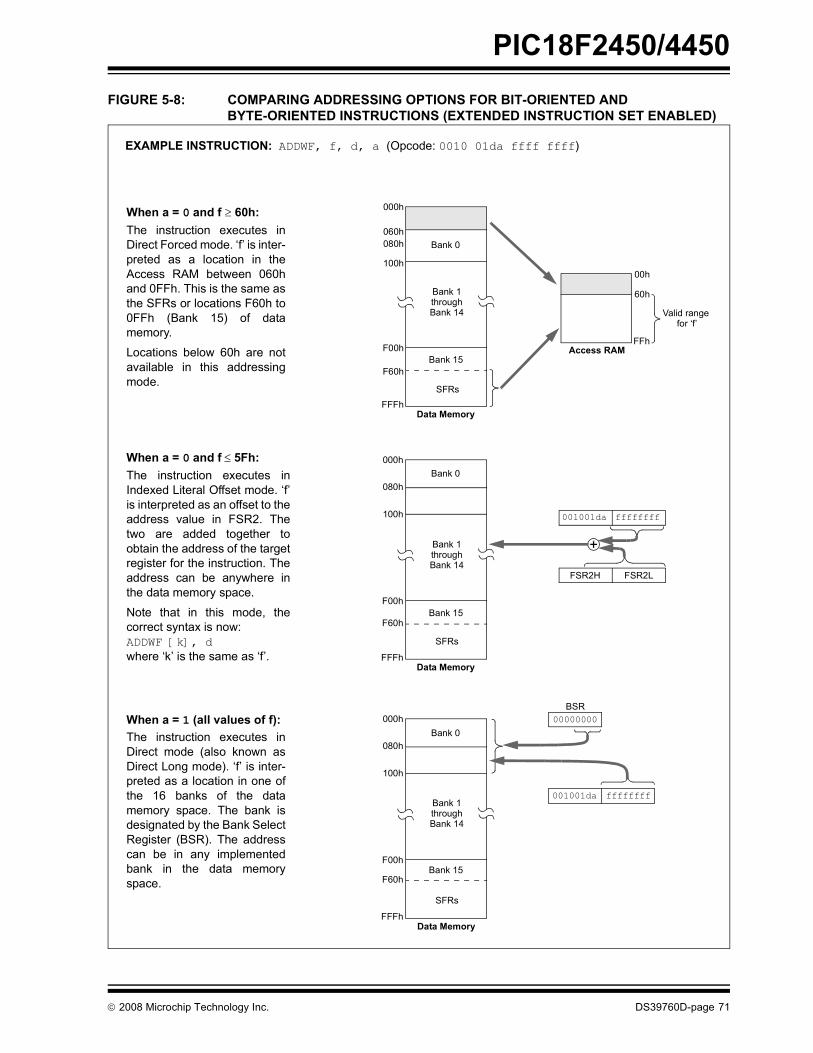
PIC18F2450/4450
© 2008 Microchip Technology Inc. DS39760D-page 71
FIGURE 5-8: COMPARING ADDRESSING OPTIONS FOR BIT-ORIENTED AND BYTE-ORIENTED INSTRUCTIONS (EXTENDED INSTRUCTION SET ENABLED)
EXAMPLE INSTRUCTION: ADDWF, f, d, a (Opcode: 0010 01da ffff ffff)
When a = 0 and f ≥ 60h:The instruction executes inDirect Forced mode. �f� is inter-preted as a location in theAccess RAM between 060hand 0FFh. This is the same asthe SFRs or locations F60h to0FFh (Bank 15) of datamemory.
Locations below 60h are notavailable in this addressingmode.
When a = 0 and f ≤ 5Fh:The instruction executes inIndexed Literal Offset mode. �f�is interpreted as an offset to theaddress value in FSR2. Thetwo are added together toobtain the address of the targetregister for the instruction. Theaddress can be anywhere inthe data memory space.
Note that in this mode, thecorrect syntax is now:ADDWF [k], dwhere �k� is the same as �f�.
When a = 1 (all values of f):The instruction executes inDirect mode (also known asDirect Long mode). �f� is inter-preted as a location in one ofthe 16 banks of the datamemory space. The bank isdesignated by the Bank SelectRegister (BSR). The addresscan be in any implementedbank in the data memoryspace.
000h
060h
100h
F00h
F60h
FFFh
Valid range
00h
60h
FFh
Data Memory
Access RAM
Bank 0
Bank 1throughBank 14
Bank 15
SFRs
000h
080h
100h
F00h
F60h
FFFhData Memory
Bank 0
Bank 1throughBank 14
Bank 15
SFRs
FSR2H FSR2L
ffffffff001001da
ffffffff001001da
000h
080h
100h
F00h
F60h
FFFhData Memory
Bank 0
Bank 1throughBank 14
Bank 15
SFRs
for �f�
BSR00000000
080h

PIC18F2450/4450
DS39760D-page 72 © 2008 Microchip Technology Inc.
5.6.3 MAPPING THE ACCESS BANK IN INDEXED LITERAL OFFSET MODE
The use of Indexed Literal Offset Addressing modeeffectively changes how the lower portion of AccessRAM (00h to 5Fh) is mapped. Rather than containingjust the contents of the bottom half of Bank 0, this modemaps the contents from Bank 0 and a user-defined�window� that can be located anywhere in the datamemory space. The value of FSR2 establishes thelower boundary of the addresses mapped into thewindow, while the upper boundary is defined by FSR2plus 95 (5Fh). Addresses in the Access RAM above5Fh are mapped as previously described (seeSection 5.3.3 �Access Bank�). An example of AccessBank remapping in this addressing mode is shown inFigure 5-9.
Remapping of the Access Bank applies only tooperations using the Indexed Literal Offset mode.Operations that use the BSR (Access RAM bit is �1�) willcontinue to use Direct Addressing as before. Anyindirect or indexed operation that explicitly uses any ofthe indirect file operands (including FSR2) will continueto operate as standard Indirect Addressing. Anyinstruction that uses the Access Bank, but includes aregister address of greater than 05Fh, will use DirectAddressing and the normal Access Bank map.
5.6.4 BSR IN INDEXED LITERAL OFFSET MODE
Although the Access Bank is remapped when theextended instruction set is enabled, the operation of theBSR remains unchanged. Direct Addressing, using theBSR to select the data memory bank, operates in thesame manner as previously described.
FIGURE 5-9: REMAPPING THE ACCESS BANK WITH INDEXED LITERAL OFFSET ADDRESSING
Data Memory
000h
100h
200h
F60h
F00h
FFFh
Bank 1
Bank 15
Bank 2throughBank 14
SFRs
ADDWF f, d, aFSR2H:FSR2L = 120h
Locations in the regionfrom the FSR2 Pointer(120h) to the pointer plus05Fh (17Fh) are mappedto the bottom of theAccess RAM (000h-05Fh).
Special Function Registersat F60h through FFFh aremapped to 60h throughFFh as usual.
Bank 0 addresses below5Fh are not available inthis mode. They can stillbe addressed by using theBSR.
Access Bank
00h
60h
FFh
Bank 0
SFRs
Bank 1 �Window�
Window
Example Situation:
120h17Fh
5Fh
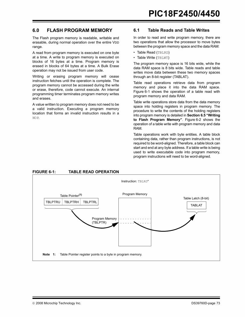
PIC18F2450/4450
© 2008 Microchip Technology Inc. DS39760D-page 73
6.0 FLASH PROGRAM MEMORYThe Flash program memory is readable, writable anderasable, during normal operation over the entire VDDrange.
A read from program memory is executed on one byteat a time. A write to program memory is executed onblocks of 16 bytes at a time. Program memory iserased in blocks of 64 bytes at a time. A Bulk Eraseoperation may not be issued from user code.
Writing or erasing program memory will ceaseinstruction fetches until the operation is complete. Theprogram memory cannot be accessed during the writeor erase, therefore, code cannot execute. An internalprogramming timer terminates program memory writesand erases.
A value written to program memory does not need to bea valid instruction. Executing a program memorylocation that forms an invalid instruction results in aNOP.
6.1 Table Reads and Table WritesIn order to read and write program memory, there aretwo operations that allow the processor to move bytesbetween the program memory space and the data RAM:
� Table Read (TBLRD)� Table Write (TBLWT)
The program memory space is 16 bits wide, while thedata RAM space is 8 bits wide. Table reads and tablewrites move data between these two memory spacesthrough an 8-bit register (TABLAT).
Table read operations retrieve data from programmemory and place it into the data RAM space.Figure 6-1 shows the operation of a table read withprogram memory and data RAM.
Table write operations store data from the data memoryspace into holding registers in program memory. Theprocedure to write the contents of the holding registersinto program memory is detailed in Section 6.5 �Writingto Flash Program Memory�. Figure 6-2 shows theoperation of a table write with program memory and dataRAM.
Table operations work with byte entities. A table blockcontaining data, rather than program instructions, is notrequired to be word-aligned. Therefore, a table block canstart and end at any byte address. If a table write is beingused to write executable code into program memory,program instructions will need to be word-aligned.
FIGURE 6-1: TABLE READ OPERATION
Table Pointer(1)Table Latch (8-bit)
Program Memory
TBLPTRH TBLPTRLTABLAT
TBLPTRU
Instruction: TBLRD*
Note 1: Table Pointer register points to a byte in program memory.
Program Memory(TBLPTR)

PIC18F2450/4450
DS39760D-page 74 © 2008 Microchip Technology Inc.
FIGURE 6-2: TABLE WRITE OPERATION
6.2 Control RegistersSeveral control registers are used in conjunction withthe TBLRD and TBLWT instructions. These include the:
� EECON1 register� EECON2 register� TABLAT register� TBLPTR registers
6.2.1 EECON1 AND EECON2 REGISTERSThe EECON1 register (Register 6-1) is the controlregister for memory accesses. The EECON2 register isnot a physical register; it is used exclusively in thememory write and erase sequences. ReadingEECON2 will read all �0�s.
The CFGS control bit determines if the access will beto the Configuration/Calibration registers or to programmemory.
The FREE bit, when set, will allow a program memoryerase operation. When FREE is set, the eraseoperation is initiated on the next WR command. WhenFREE is clear, only writes are enabled.
The WREN bit, when set, will allow a write operation.On power-up, the WREN bit is clear. The WRERR bit isset in hardware when the WREN bit is set and clearedwhen the internal programming timer expires and thewrite operation is complete.
The WR control bit initiates write operations. The bitcannot be cleared, only set, in software; it is cleared inhardware at the completion of the write operation.
Table Pointer(1) Table Latch (8-bit)
TBLPTRH TBLPTRL TABLAT
Program Memory(TBLPTR)
TBLPTRU
Instruction: TBLWT*
Note 1: Table Pointer actually points to one of 16 holding registers, the address of which is determined by TBLPTRL<3:0>. The process for physically writing data to the program memory array is discussed in Section 6.5 �Writing to Flash Program Memory�.
Holding Registers Program Memory
Note: During normal operation, the WRERR isread as �1�. This can indicate that a writeoperation was prematurely terminated bya Reset or a write operation wasattempted improperly.
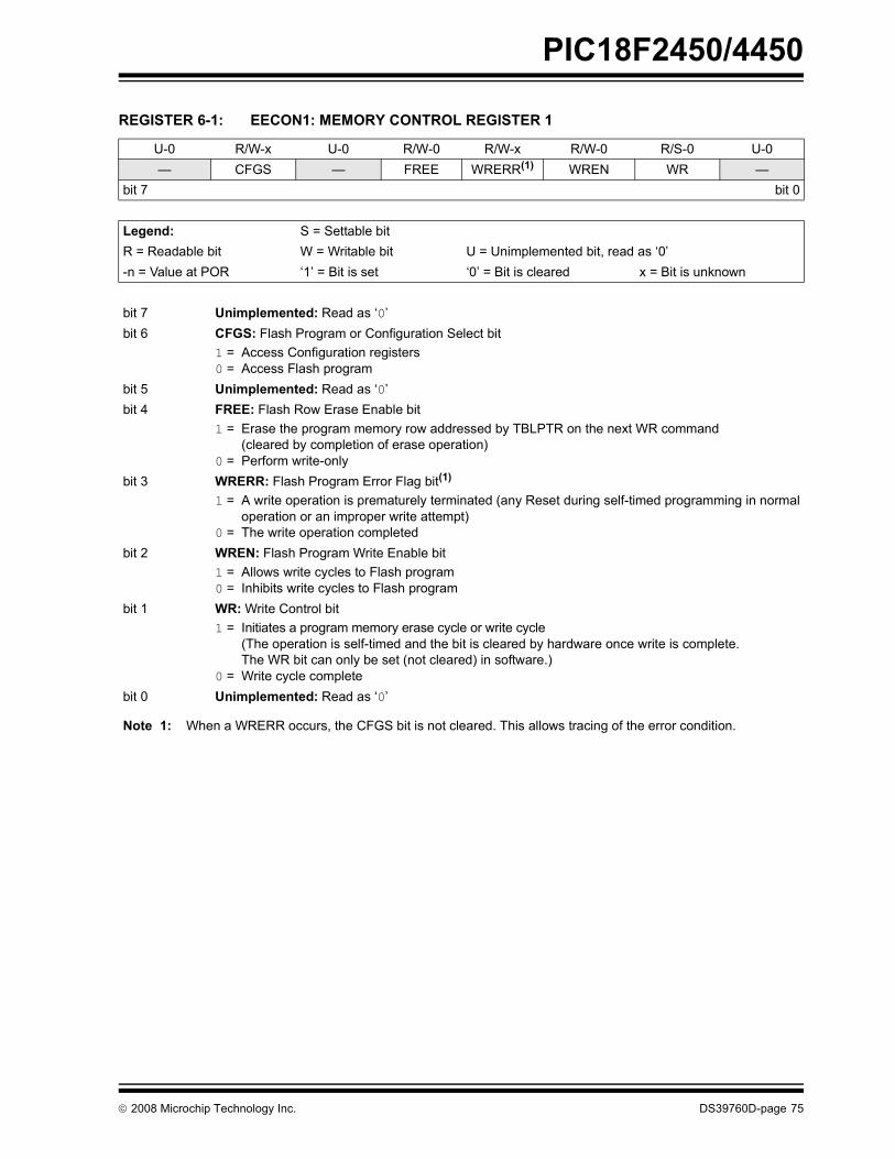
PIC18F2450/4450
© 2008 Microchip Technology Inc. DS39760D-page 75
REGISTER 6-1: EECON1: MEMORY CONTROL REGISTER 1
U-0 R/W-x U-0 R/W-0 R/W-x R/W-0 R/S-0 U-0� CFGS � FREE WRERR(1) WREN WR �
bit 7 bit 0
Legend: S = Settable bitR = Readable bit W = Writable bit U = Unimplemented bit, read as �0�-n = Value at POR �1� = Bit is set �0� = Bit is cleared x = Bit is unknown
bit 7 Unimplemented: Read as �0�bit 6 CFGS: Flash Program or Configuration Select bit
1 = Access Configuration registers0 = Access Flash program
bit 5 Unimplemented: Read as �0�bit 4 FREE: Flash Row Erase Enable bit
1 = Erase the program memory row addressed by TBLPTR on the next WR command (cleared by completion of erase operation)
0 = Perform write-onlybit 3 WRERR: Flash Program Error Flag bit(1)
1 = A write operation is prematurely terminated (any Reset during self-timed programming in normaloperation or an improper write attempt)
0 = The write operation completedbit 2 WREN: Flash Program Write Enable bit
1 = Allows write cycles to Flash program0 = Inhibits write cycles to Flash program
bit 1 WR: Write Control bit1 = Initiates a program memory erase cycle or write cycle
(The operation is self-timed and the bit is cleared by hardware once write is complete. The WR bit can only be set (not cleared) in software.)
0 = Write cycle completebit 0 Unimplemented: Read as �0�
Note 1: When a WRERR occurs, the CFGS bit is not cleared. This allows tracing of the error condition.

PIC18F2450/4450
DS39760D-page 76 © 2008 Microchip Technology Inc.
6.2.2 TABLE LATCH REGISTER (TABLAT)The Table Latch (TABLAT) is an 8-bit register mappedinto the SFR space. The Table Latch register is used tohold 8-bit data during data transfers between programmemory and data RAM.
6.2.3 TABLE POINTER REGISTER (TBLPTR)
The Table Pointer (TBLPTR) register addresses a bytewithin the program memory. The TBLPTR is comprisedof three SFR registers: Table Pointer Upper Byte, TablePointer High Byte and Table Pointer Low Byte(TBLPTRU:TBLPTRH:TBLPTRL). These three registersjoin to form a 22-bit wide pointer. The low-order 21 bitsallow the device to address up to 2 Mbytes of programmemory space. The 22nd bit allows access to the deviceID, the user ID and the Configuration bits.
The Table Pointer, TBLPTR, is used by the TBLRD andTBLWT instructions. These instructions can update theTBLPTR in one of four ways based on the table opera-tion. These operations are shown in Table 6-1. Theseoperations on the TBLPTR only affect the low-order21 bits.
6.2.4 TABLE POINTER BOUNDARIESTBLPTR is used in reads, writes and erases of theFlash program memory.
When a TBLRD is executed, all 22 bits of the TBLPTRdetermine which byte is read from program memoryinto TABLAT.
When a TBLWT is executed, the four LSbs of the TablePointer register (TBLPTR<3:0>) determine which of the16 program memory holding registers is written to.When the timed write to program memory begins (viathe WR bit), the 16 MSbs of the TBLPTR(TBLPTR<21:4>) determine which program memoryblock of 16 bytes is written to. For more detail, seeSection 6.5 �Writing to Flash Program Memory�.
When an erase of program memory is executed, the16 MSbs of the Table Pointer register (TBLPTR<21:6>)point to the 64-byte block that will be erased. The LeastSignificant bits (TBLPTR<5:0>) are ignored.
Figure 6-3 describes the relevant boundaries of theTBLPTR based on Flash program memory operations.
TABLE 6-1: TABLE POINTER OPERATIONS WITH TBLRD AND TBLWT INSTRUCTIONS
FIGURE 6-3: TABLE POINTER BOUNDARIES BASED ON OPERATION
Example Operation on Table Pointer
TBLRD*TBLWT*
TBLPTR is not modified
TBLRD*+TBLWT*+
TBLPTR is incremented after the read/write
TBLRD*-TBLWT*-
TBLPTR is decremented after the read/write
TBLRD+*TBLWT+*
TBLPTR is incremented before the read/write
21 16 15 8 7 0
TABLE ERASE
TABLE READ � TBLPTR<21:0>
TBLPTRLTBLPTRHTBLPTRU
TBLPTR<21:6>
TABLE WRITE � TBLPTR<21:4>

PIC18F2450/4450
© 2008 Microchip Technology Inc. DS39760D-page 77
6.3 Reading the Flash Program Memory
The TBLRD instruction is used to retrieve data fromprogram memory and places it into data RAM. Tablereads from program memory are performed one byte ata time.
TBLPTR points to a byte address in program space.Executing TBLRD places the byte pointed to intoTABLAT. In addition, TBLPTR can be modifiedautomatically for the next table read operation.
The internal program memory is typically organized bywords. The Least Significant bit of the address selectsbetween the high and low bytes of the word. Figure 6-4shows the interface between the internal programmemory and the TABLAT.
FIGURE 6-4: READS FROM FLASH PROGRAM MEMORY
EXAMPLE 6-1: READING A FLASH PROGRAM MEMORY WORD
(Even Byte Address)
Program Memory
(Odd Byte Address)
TBLRD TABLAT
TBLPTR = xxxxx1
FETCHInstruction Register
(IR) Read Register
TBLPTR = xxxxx0
MOVLW CODE_ADDR_UPPER ; Load TBLPTR with the baseMOVWF TBLPTRU ; address of the wordMOVLW CODE_ADDR_HIGHMOVWF TBLPTRHMOVLW CODE_ADDR_LOWMOVWF TBLPTRL
READ_WORDTBLRD*+ ; read into TABLAT and incrementMOVF TABLAT, W ; get dataMOVWF WORD_EVENTBLRD*+ ; read into TABLAT and incrementMOVF TABLAT, W ; get dataMOVF WORD_ODD
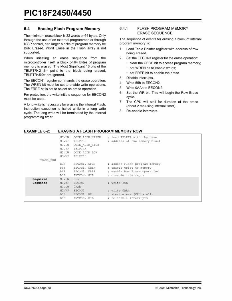
PIC18F2450/4450
DS39760D-page 78 © 2008 Microchip Technology Inc.
6.4 Erasing Flash Program MemoryThe minimum erase block is 32 words or 64 bytes. Onlythrough the use of an external programmer, or throughICSP control, can larger blocks of program memory beBulk Erased. Word Erase in the Flash array is notsupported.
When initiating an erase sequence from themicrocontroller itself, a block of 64 bytes of programmemory is erased. The Most Significant 16 bits of theTBLPTR<21:6> point to the block being erased.TBLPTR<5:0> are ignored.
The EECON1 register commands the erase operation.The WREN bit must be set to enable write operations.The FREE bit is set to select an erase operation.
For protection, the write initiate sequence for EECON2must be used.
A long write is necessary for erasing the internal Flash.Instruction execution is halted while in a long writecycle. The long write will be terminated by the internalprogramming timer.
6.4.1 FLASH PROGRAM MEMORY ERASE SEQUENCE
The sequence of events for erasing a block of internalprogram memory is:
1. Load Table Pointer register with address of rowbeing erased.
2. Set the EECON1 register for the erase operation:� clear the CFGS bit to access program memory;� set WREN bit to enable writes; � set FREE bit to enable the erase.
3. Disable interrupts.4. Write 55h to EECON2.5. Write 0AAh to EECON2.6. Set the WR bit. This will begin the Row Erase
cycle.7. The CPU will stall for duration of the erase
(about 2 ms using internal timer).8. Re-enable interrupts.
EXAMPLE 6-2: ERASING A FLASH PROGRAM MEMORY ROW MOVLW CODE_ADDR_UPPER ; load TBLPTR with the baseMOVWF TBLPTRU ; address of the memory blockMOVLW CODE_ADDR_HIGHMOVWF TBLPTRH MOVLW CODE_ADDR_LOWMOVWF TBLPTRL
ERASE_ROW BCF EECON1, CFGS ; access Flash program memoryBSF EECON1, WREN ; enable write to memoryBSF EECON1, FREE ; enable Row Erase operationBCF INTCON, GIE ; disable interrupts
Required MOVLW 55hSequence MOVWF EECON2 ; write 55h
MOVLW 0AAhMOVWF EECON2 ; write 0AAhBSF EECON1, WR ; start erase (CPU stall)BSF INTCON, GIE ; re-enable interrupts
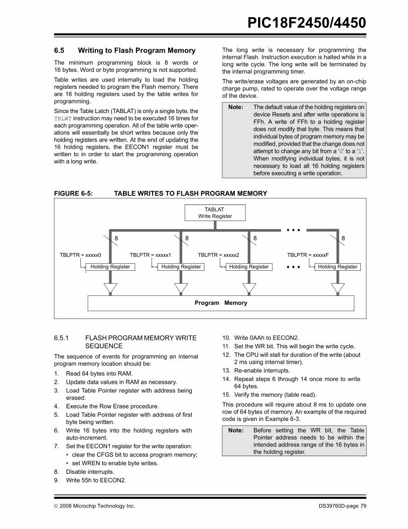
PIC18F2450/4450
© 2008 Microchip Technology Inc. DS39760D-page 79
6.5 Writing to Flash Program MemoryThe minimum programming block is 8 words or16 bytes. Word or byte programming is not supported.Table writes are used internally to load the holdingregisters needed to program the Flash memory. Thereare 16 holding registers used by the table writes forprogramming.Since the Table Latch (TABLAT) is only a single byte, theTBLWT instruction may need to be executed 16 times foreach programming operation. All of the table write oper-ations will essentially be short writes because only theholding registers are written. At the end of updating the16 holding registers, the EECON1 register must bewritten to in order to start the programming operationwith a long write.
The long write is necessary for programming theinternal Flash. Instruction execution is halted while in along write cycle. The long write will be terminated bythe internal programming timer. The write/erase voltages are generated by an on-chipcharge pump, rated to operate over the voltage rangeof the device.
FIGURE 6-5: TABLE WRITES TO FLASH PROGRAM MEMORY
6.5.1 FLASH PROGRAM MEMORY WRITE SEQUENCE
The sequence of events for programming an internalprogram memory location should be:1. Read 64 bytes into RAM.2. Update data values in RAM as necessary.3. Load Table Pointer register with address being
erased.4. Execute the Row Erase procedure.5. Load Table Pointer register with address of first
byte being written.6. Write 16 bytes into the holding registers with
auto-increment.7. Set the EECON1 register for the write operation:
� clear the CFGS bit to access program memory;� set WREN to enable byte writes.
8. Disable interrupts.9. Write 55h to EECON2.
10. Write 0AAh to EECON2.11. Set the WR bit. This will begin the write cycle.12. The CPU will stall for duration of the write (about
2 ms using internal timer).13. Re-enable interrupts.14. Repeat steps 6 through 14 once more to write
64 bytes.15. Verify the memory (table read).This procedure will require about 8 ms to update onerow of 64 bytes of memory. An example of the requiredcode is given in Example 6-3.
Note: The default value of the holding registers ondevice Resets and after write operations isFFh. A write of FFh to a holding registerdoes not modify that byte. This means thatindividual bytes of program memory may bemodified, provided that the change does notattempt to change any bit from a �0� to a �1�.When modifying individual bytes, it is notnecessary to load all 16 holding registersbefore executing a write operation.
TBLPTR = xxxxxFTBLPTR = xxxxx1TBLPTR = xxxxx0 TBLPTR = xxxxx2
Program Memory
Holding Register Holding Register Holding Register Holding Register
8 8 8 8
TABLAT Write Register
Note: Before setting the WR bit, the TablePointer address needs to be within theintended address range of the 16 bytes inthe holding register.

PIC18F2450/4450
DS39760D-page 80 © 2008 Microchip Technology Inc.
EXAMPLE 6-3: WRITING TO FLASH PROGRAM MEMORYMOVLW D'64� ; number of bytes in erase blockMOVWF COUNTERMOVLW BUFFER_ADDR_HIGH ; point to bufferMOVWF FSR0HMOVLW BUFFER_ADDR_LOWMOVWF FSR0LMOVLW CODE_ADDR_UPPER ; Load TBLPTR with the baseMOVWF TBLPTRU ; address of the memory blockMOVLW CODE_ADDR_HIGHMOVWF TBLPTRHMOVLW CODE_ADDR_LOWMOVWF TBLPTRL
READ_BLOCKTBLRD*+ ; read into TABLAT, and incMOVF TABLAT, W ; get dataMOVWF POSTINC0 ; store dataDECFSZ COUNTER ; done?BRA READ_BLOCK ; repeat
MODIFY_WORDMOVLW DATA_ADDR_HIGH ; point to bufferMOVWF FSR0HMOVLW DATA_ADDR_LOWMOVWF FSR0LMOVLW NEW_DATA_LOW ; update buffer wordMOVWF POSTINC0MOVLW NEW_DATA_HIGHMOVWF INDF0
ERASE_BLOCKMOVLW CODE_ADDR_UPPER ; load TBLPTR with the baseMOVWF TBLPTRU ; address of the memory blockMOVLW CODE_ADDR_HIGHMOVWF TBLPTRH MOVLW CODE_ADDR_LOWMOVWF TBLPTRL BCF EECON1, CFGS ; access Flash program memoryBSF EECON1, WREN ; enable write to memoryBSF EECON1, FREE ; enable Row Erase operationBCF INTCON, GIE ; disable interrupts
MOVLW 55hRequired MOVWF EECON2 ; write 55hSequence MOVLW 0AAh
MOVWF EECON2 ; write 0AAhBSF EECON1, WR ; start erase (CPU stall)BSF INTCON, GIE ; re-enable interruptsTBLRD*- ; dummy read decrementMOVLW BUFFER_ADDR_HIGH ; point to bufferMOVWF FSR0HMOVLW BUFFER_ADDR_LOWMOVWF FSR0LMOVLW D�4�MOVWF COUNTER1
WRITE_BUFFER_BACKMOVLW D�16� ; number of bytes in holding registerMOVWF COUNTER
WRITE_BYTE_TO_HREGSMOVF POSTINC0, W ; get low byte of buffer dataMOVWF TABLAT ; present data to table latchTBLWT+* ; write data, perform a short write
; to internal TBLWT holding register.DECFSZ COUNTER ; loop until buffers are fullBRA WRITE_WORD_TO_HREGS
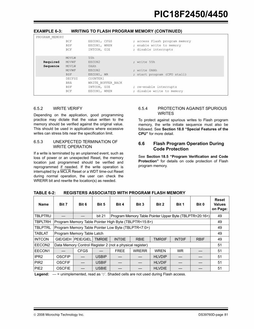
PIC18F2450/4450
© 2008 Microchip Technology Inc. DS39760D-page 81
EXAMPLE 6-3: WRITING TO FLASH PROGRAM MEMORY (CONTINUED)
6.5.2 WRITE VERIFYDepending on the application, good programmingpractice may dictate that the value written to thememory should be verified against the original value.This should be used in applications where excessivewrites can stress bits near the specification limit.
6.5.3 UNEXPECTED TERMINATION OF WRITE OPERATION
If a write is terminated by an unplanned event, such asloss of power or an unexpected Reset, the memorylocation just programmed should be verified andreprogrammed if needed. If the write operation isinterrupted by a MCLR Reset or a WDT time-out Resetduring normal operation, the user can check theWRERR bit and rewrite the location(s) as needed.
6.5.4 PROTECTION AGAINST SPURIOUS WRITES
To protect against spurious writes to Flash programmemory, the write initiate sequence must also befollowed. See Section 18.0 �Special Features of theCPU� for more detail.
6.6 Flash Program Operation During Code Protection
See Section 18.5 �Program Verification and CodeProtection� for details on code protection of Flashprogram memory.
TABLE 6-2: REGISTERS ASSOCIATED WITH PROGRAM FLASH MEMORY
PROGRAM_MEMORYBCF EECON1, CFGS ; access Flash program memoryBSF EECON1, WREN ; enable write to memoryBCF INTCON, GIE ; disable interrupts
MOVLW 55hRequired MOVWF EECON2 ; write 55hSequence MOVLW 0AAh
MOVWF EECON2 ; write 0AAhBSF EECON1, WR ; start program (CPU stall)DECFSZ COUNTER1BRA WRITE_BUFFER_BACKBSF INTCON, GIE ; re-enable interruptsBCF EECON1, WREN ; disable write to memory
Name Bit 7 Bit 6 Bit 5 Bit 4 Bit 3 Bit 2 Bit 1 Bit 0Reset Values
on Page:
TBLPTRU � � bit 21 Program Memory Table Pointer Upper Byte (TBLPTR<20:16>) 49TBPLTRH Program Memory Table Pointer High Byte (TBLPTR<15:8>) 49TBLPTRL Program Memory Table Pointer Low Byte (TBLPTR<7:0>) 49TABLAT Program Memory Table Latch 49INTCON GIE/GIEH PEIE/GIEL TMR0IE INT0IE RBIE TMR0IF INT0IF RBIF 49EECON2 Data Memory Control Register 2 (not a physical register) 51EECON1 � CFGS � FREE WRERR WREN WR � 51IPR2 OSCFIP � USBIP � � HLVDIP � � 51PIR2 OSCFIF � USBIF � � HLVDIF � � 51PIE2 OSCFIE � USBIE � � HLVDIE � � 51Legend: � = unimplemented, read as �0�. Shaded cells are not used during Flash access.

PIC18F2450/4450
DS39760D-page 82 © 2008 Microchip Technology Inc.
NOTES:

PIC18F2450/4450
© 2008 Microchip Technology Inc. DS39760D-page 83
7.0 8 x 8 HARDWARE MULTIPLIER
7.1 IntroductionAll PIC18 devices include an 8 x 8 hardware multiplieras part of the ALU. The multiplier performs an unsignedoperation and yields a 16-bit result that is stored in theproduct register pair, PRODH:PRODL. The multiplier�soperation does not affect any flags in the STATUSregister.
Making multiplication a hardware operation allows it tobe completed in a single instruction cycle. This has theadvantages of higher computational throughput andreduced code size for multiplication algorithms andallows the PIC18 devices to be used in many applica-tions previously reserved for digital signal processors.A comparison of various hardware and softwaremultiply operations, along with the savings in memoryand execution time, is shown in Table 7-1.
7.2 OperationExample 7-1 shows the instruction sequence for an8 x 8 unsigned multiplication. Only one instruction isrequired when one of the arguments is already loadedin the WREG register.
Example 7-2 shows the sequence to do an 8 x 8 signedmultiplication. To account for the sign bits of thearguments, each argument�s Most Significant bit (MSb)is tested and the appropriate subtractions are done.
EXAMPLE 7-1: 8 x 8 UNSIGNED MULTIPLY ROUTINE
EXAMPLE 7-2: 8 x 8 SIGNED MULTIPLY ROUTINE
TABLE 7-1: PERFORMANCE COMPARISON FOR VARIOUS MULTIPLY OPERATIONS
MOVF ARG1, W ; MULWF ARG2 ; ARG1 * ARG2 ->
; PRODH:PRODL
MOVF ARG1, W MULWF ARG2 ; ARG1 * ARG2 ->
; PRODH:PRODL BTFSC ARG2, SB ; Test Sign Bit SUBWF PRODH, F ; PRODH = PRODH
; - ARG1 MOVF ARG2, WBTFSC ARG1, SB ; Test Sign Bit SUBWF PRODH, F ; PRODH = PRODH
; - ARG2
Routine Multiply MethodProgramMemory(Words)
Cycles(Max)
Time
@ 40 MHz @ 10 MHz @ 4 MHz
8 x 8 unsignedWithout hardware multiply 13 69 6.9 μs 27.6 μs 69 μs
Hardware multiply 1 1 100 ns 400 ns 1 μs
8 x 8 signedWithout hardware multiply 33 91 9.1 μs 36.4 μs 91 μs
Hardware multiply 6 6 600 ns 2.4 μs 6 μs
16 x 16 unsignedWithout hardware multiply 21 242 24.2 μs 96.8 μs 242 μs
Hardware multiply 28 28 2.8 μs 11.2 μs 28 μs
16 x 16 signedWithout hardware multiply 52 254 25.4 μs 102.6 μs 254 μs
Hardware multiply 35 40 4.0 μs 16.0 μs 40 μs

PIC18F2450/4450
DS39760D-page 84 © 2008 Microchip Technology Inc.
Example 7-3 shows the sequence to do a 16 x 16unsigned multiplication. Equation 7-1 shows thealgorithm that is used. The 32-bit result is stored in fourregisters (RES3:RES0).
EQUATION 7-1: 16 x 16 UNSIGNED MULTIPLICATION ALGORITHM
EXAMPLE 7-3: 16 x 16 UNSIGNED MULTIPLY ROUTINE
Example 7-4 shows the sequence to do a 16 x 16signed multiply. Equation 7-2 shows the algorithmused. The 32-bit result is stored in four registers(RES3:RES0). To account for the sign bits of thearguments, the MSb for each argument pair is testedand the appropriate subtractions are done.
EQUATION 7-2: 16 x 16 SIGNED MULTIPLICATION ALGORITHM
EXAMPLE 7-4: 16 x 16 SIGNED MULTIPLY ROUTINE
RES3:RES0 = ARG1H:ARG1L • ARG2H:ARG2L= (ARG1H • ARG2H • 216) +
(ARG1H • ARG2L • 28) +(ARG1L • ARG2H • 28) +(ARG1L • ARG2L)
MOVF ARG1L, W MULWF ARG2L ; ARG1L * ARG2L->
; PRODH:PRODL MOVFF PRODH, RES1 ; MOVFF PRODL, RES0 ;
; MOVF ARG1H, W MULWF ARG2H ; ARG1H * ARG2H->
; PRODH:PRODL MOVFF PRODH, RES3 ; MOVFF PRODL, RES2 ;
; MOVF ARG1L, W MULWF ARG2H ; ARG1L * ARG2H->
; PRODH:PRODL MOVF PRODL, W ;ADDWF RES1, F ; Add cross MOVF PRODH, W ; products ADDWFC RES2, F ; CLRF WREG ; ADDWFC RES3, F ;
; MOVF ARG1H, W ; MULWF ARG2L ; ARG1H * ARG2L->
; PRODH:PRODL MOVF PRODL, W ; ADDWF RES1, F ; Add cross MOVF PRODH, W ; products ADDWFC RES2, F ; CLRF WREG ; ADDWFC RES3, F ;
RES3:RES0= ARG1H:ARG1L • ARG2H:ARG2L= (ARG1H • ARG2H • 216) +
(ARG1H • ARG2L • 28) +(ARG1L • ARG2H • 28) +(ARG1L • ARG2L) +(-1 • ARG2H<7> • ARG1H:ARG1L • 216) +(-1 • ARG1H<7> • ARG2H:ARG2L • 216)
MOVF ARG1L, W MULWF ARG2L ; ARG1L * ARG2L ->
; PRODH:PRODL MOVFF PRODH, RES1 ; MOVFF PRODL, RES0 ;
; MOVF ARG1H, W MULWF ARG2H ; ARG1H * ARG2H ->
; PRODH:PRODL MOVFF PRODH, RES3 ; MOVFF PRODL, RES2 ;
; MOVF ARG1L,W MULWF ARG2H ; ARG1L * ARG2H ->
; PRODH:PRODL MOVF PRODL, W ; ADDWF RES1, F ; Add cross MOVF PRODH, W ; products ADDWFC RES2, F ; CLRF WREG ; ADDWFC RES3, F ;
; MOVF ARG1H, W ; MULWF ARG2L ; ARG1H * ARG2L ->
; PRODH:PRODL MOVF PRODL, W ; ADDWF RES1, F ; Add cross MOVF PRODH, W ; products ADDWFC RES2, F ; CLRF WREG ; ADDWFC RES3, F ;
; BTFSS ARG2H, 7 ; ARG2H:ARG2L neg? BRA SIGN_ARG1 ; no, check ARG1 MOVF ARG1L, W ; SUBWF RES2 ; MOVF ARG1H, W ; SUBWFB RES3
; SIGN_ARG1
BTFSS ARG1H, 7 ; ARG1H:ARG1L neg? BRA CONT_CODE ; no, done MOVF ARG2L, W ; SUBWF RES2 ; MOVF ARG2H, W ; SUBWFB RES3
; CONT_CODE :

PIC18F2450/4450
© 2008 Microchip Technology Inc. DS39760D-page 85
8.0 INTERRUPTSThe PIC18F2450/4450 devices have multiple interruptsources and an interrupt priority feature that allowseach interrupt source to be assigned a high-prioritylevel or a low-priority level. The high-priority interruptvector is at 000008h and the low-priority interrupt vec-tor is at 000018h. High-priority interrupt events willinterrupt any low-priority interrupts that may be inprogress.
There are ten registers which are used to controlinterrupt operation. These registers are:
� RCON� INTCON� INTCON2� INTCON3� PIR1, PIR2� PIE1, PIE2� IPR1, IPR2
It is recommended that the Microchip header filessupplied with MPLAB® IDE be used for the symbolic bitnames in these registers. This allows the assembler/compiler to automatically take care of the placement ofthese bits within the specified register.
Each interrupt source has three bits to control itsoperation. The functions of these bits are:
� Flag bit to indicate that an interrupt event occurred
� Enable bit that allows program execution to branch to the interrupt vector address when the flag bit is set
� Priority bit to select high priority or low priority
The interrupt priority feature is enabled by setting theIPEN bit (RCON<7>). When interrupt priority isenabled, there are two bits which enable interruptsglobally. Setting the GIEH bit (INTCON<7>) enables allinterrupts that have the priority bit set (high priority).Setting the GIEL bit (INTCON<6>) enables allinterrupts that have the priority bit cleared (low priority).When the interrupt flag, enable bit and appropriateglobal interrupt enable bit are set, the interrupt willvector immediately to address 000008h or 000018h,depending on the priority bit setting. Individual inter-rupts can be disabled through their correspondingenable bits.
When the IPEN bit is cleared (default state), theinterrupt priority feature is disabled and interrupts arecompatible with PIC® mid-range microcontrollers. InCompatibility mode, the interrupt priority bits for eachsource have no effect. INTCON<6> is the PEIE bitwhich enables/disables all peripheral interrupt sources.INTCON<7> is the GIE bit which enables/disables allinterrupt sources. All interrupts branch to address000008h in Compatibility mode.
When an interrupt is responded to, the global interruptenable bit is cleared to disable further interrupts. If theIPEN bit is cleared, this is the GIE bit. If interrupt prioritylevels are used, this will be either the GIEH or GIEL bit.High-priority interrupt sources can interrupt a low-priority interrupt. Low-priority interrupts are notprocessed while high-priority interrupts are in progress.
The return address is pushed onto the stack and the PCis loaded with the interrupt vector address (000008h or000018h). Once in the Interrupt Service Routine, thesource(s) of the interrupt can be determined by pollingthe interrupt flag bits. The interrupt flag bits must becleared in software before re-enabling interrupts to avoidrecursive interrupts.
The �return from interrupt� instruction, RETFIE, exitsthe interrupt routine and sets the GIE bit (GIEH or GIELif priority levels are used) which re-enables interrupts.
For external interrupt events, such as the INTx pins orthe PORTB input change interrupt, the interrupt latencywill be three to four instruction cycles. The exactlatency is the same for one or two-cycle instructions.Individual interrupt flag bits are set regardless of thestatus of their corresponding enable bit or the GIE bit.
8.1 USB InterruptsUnlike other peripherals, the USB module is capable ofgenerating a wide range of interrupts for many types ofevents. These include several types of normal commu-nication and status events and several module levelerror events.
To handle these events, the USB module is equippedwith its own interrupt logic. The logic functions in amanner similar to the microcontroller level interruptfunnel, with each interrupt source having separate flagand enable bits. All events are funneled to a singledevice level interrupt, USBIF (PIR2<5>). Unlike thedevice level interrupt logic, the individual USB interruptevents cannot be individually assigned their own prior-ity. This is determined at the device level interruptfunnel for all USB events by the USBIP bit.
For additional details on USB interrupt logic, refer toSection 14.5 �USB Interrupts�.
Note: Do not use the MOVFF instruction to modifyany of the interrupt control registers whileany interrupt is enabled. Doing so maycause erratic microcontroller behavior.

PIC18F2450/4450
DS39760D-page 86 © 2008 Microchip Technology Inc.
FIGURE 8-1: INTERRUPT LOGIC
TMR0IE
GIE/GIEH
PEIE/GIEL
Wake-up if in Sleep Mode
Interrupt to CPUVector to Location0008h
INT2IFINT2IEINT2IP
INT1IFINT1IEINT1IP
TMR0IFTMR0IETMR0IP
RBIFRBIERBIP
IPEN
TMR0IF
TMR0IP
INT1IFINT1IEINT1IPINT2IFINT2IEINT2IP
RBIFRBIERBIP
INT0IFINT0IE
PEIE/GIEL
Interrupt to CPUVector to Location
IPEN
IPEN
0018h
Peripheral Interrupt Flag bitPeripheral Interrupt Enable bitPeripheral Interrupt Priority bit
Peripheral Interrupt Flag bitPeripheral Interrupt Enable bitPeripheral Interrupt Priority bit
TMR1IFTMR1IETMR1IP
USBIFUSBIEUSBIP
Additional Peripheral Interrupts
TMR1IFTMR1IETMR1IP
High-Priority Interrupt Generation
Low-Priority Interrupt Generation
USBIFUSBIEUSBIP
Additional Peripheral Interrupts
GIE/GIEH
From USB Interrupt Logic
From USB Interrupt Logic

PIC18F2450/4450
© 2008 Microchip Technology Inc. DS39760D-page 87
8.2 INTCON RegistersThe INTCON registers are readable and writableregisters which contain various enable, priority and flagbits.
Note: Interrupt flag bits are set when an interruptcondition occurs regardless of the state ofits corresponding enable bit or the globalinterrupt enable bit. User software shouldensure the appropriate interrupt flag bitsare clear prior to enabling an interrupt.This feature allows for software polling.
REGISTER 8-1: INTCON: INTERRUPT CONTROL REGISTER
R/W-0 R/W-0 R/W-0 R/W-0 R/W-0 R/W-0 R/W-0 R/W-xGIE/GIEH PEIE/GIEL TMR0IE INT0IE RBIE TMR0IF INT0IF RBIF(1)
bit 7 bit 0
Legend:R = Readable bit W = Writable bit U = Unimplemented bit, read as �0�-n = Value at POR �1� = Bit is set �0� = Bit is cleared x = Bit is unknown
bit 7 GIE/GIEH: Global Interrupt Enable bitWhen IPEN = 0:1 = Enables all unmasked interrupts0 = Disables all interrupts When IPEN = 1:1 = Enables all high-priority interrupts 0 = Disables all interrupts
bit 6 PEIE/GIEL: Peripheral Interrupt Enable bitWhen IPEN = 0:1 = Enables all unmasked peripheral interrupts 0 = Disables all peripheral interrupts When IPEN = 1:1 = Enables all low-priority peripheral interrupts 0 = Disables all low-priority peripheral interrupts
bit 5 TMR0IE: TMR0 Overflow Interrupt Enable bit 1 = Enables the TMR0 overflow interrupt 0 = Disables the TMR0 overflow interrupt
bit 4 INT0IE: INT0 External Interrupt Enable bit 1 = Enables the INT0 external interrupt 0 = Disables the INT0 external interrupt
bit 3 RBIE: RB Port Change Interrupt Enable bit 1 = Enables the RB port change interrupt 0 = Disables the RB port change interrupt
bit 2 TMR0IF: TMR0 Overflow Interrupt Flag bit 1 = TMR0 register has overflowed (must be cleared in software) 0 = TMR0 register did not overflow
bit 1 INT0IF: INT0 External Interrupt Flag bit 1 = The INT0 external interrupt occurred (must be cleared in software) 0 = The INT0 external interrupt did not occur
bit 0 RBIF: RB Port Change Interrupt Flag bit(1) 1 = At least one of the RB7:RB4 pins changed state (must be cleared in software) 0 = None of the RB7:RB4 pins have changed state
Note 1: A mismatch condition will continue to set this bit. Reading PORTB and waiting 1 TCY will end the mismatch condition and allow the bit to be cleared.

PIC18F2450/4450
DS39760D-page 88 © 2008 Microchip Technology Inc.
REGISTER 8-2: INTCON2: INTERRUPT CONTROL REGISTER 2
R/W-1 R/W-1 R/W-1 R/W-1 U-0 R/W-1 U-0 R/W-1
RBPU INTEDG0 INTEDG1 INTEDG2 � TMR0IP � RBIPbit 7 bit 0
Legend:R = Readable bit W = Writable bit U = Unimplemented bit, read as �0�-n = Value at POR �1� = Bit is set �0� = Bit is cleared x = Bit is unknown
bit 7 RBPU: PORTB Pull-up Enable bit 1 = All PORTB pull-ups are disabled 0 = PORTB pull-ups are enabled by individual port latch values
bit 6 INTEDG0: External Interrupt 0 Edge Select bit 1 = Interrupt on rising edge 0 = Interrupt on falling edge
bit 5 INTEDG1: External Interrupt 1 Edge Select bit 1 = Interrupt on rising edge 0 = Interrupt on falling edge
bit 4 INTEDG2: External Interrupt 2 Edge Select bit 1 = Interrupt on rising edge 0 = Interrupt on falling edge
bit 3 Unimplemented: Read as �0�bit 2 TMR0IP: TMR0 Overflow Interrupt Priority bit
1 = High priority 0 = Low priority
bit 1 Unimplemented: Read as �0�bit 0 RBIP: RB Port Change Interrupt Priority bit
1 = High priority 0 = Low priority
Note: Interrupt flag bits are set when an interrupt condition occurs regardless of the state of its correspondingenable bit or the global interrupt enable bit. User software should ensure the appropriate interrupt flag bitsare clear prior to enabling an interrupt. This feature allows for software polling.
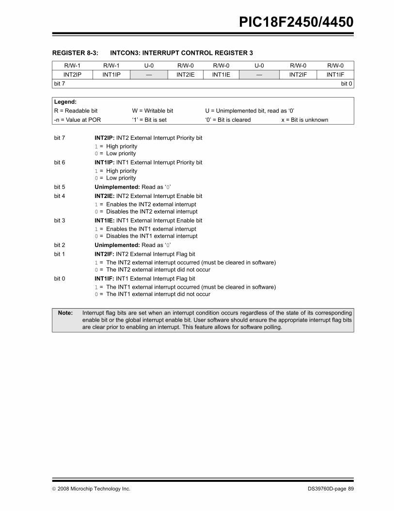
PIC18F2450/4450
© 2008 Microchip Technology Inc. DS39760D-page 89
REGISTER 8-3: INTCON3: INTERRUPT CONTROL REGISTER 3
R/W-1 R/W-1 U-0 R/W-0 R/W-0 U-0 R/W-0 R/W-0INT2IP INT1IP � INT2IE INT1IE � INT2IF INT1IF
bit 7 bit 0
Legend:R = Readable bit W = Writable bit U = Unimplemented bit, read as �0�-n = Value at POR �1� = Bit is set �0� = Bit is cleared x = Bit is unknown
bit 7 INT2IP: INT2 External Interrupt Priority bit1 = High priority 0 = Low priority
bit 6 INT1IP: INT1 External Interrupt Priority bit1 = High priority 0 = Low priority
bit 5 Unimplemented: Read as �0�bit 4 INT2IE: INT2 External Interrupt Enable bit
1 = Enables the INT2 external interrupt 0 = Disables the INT2 external interrupt
bit 3 INT1IE: INT1 External Interrupt Enable bit1 = Enables the INT1 external interrupt 0 = Disables the INT1 external interrupt
bit 2 Unimplemented: Read as �0�bit 1 INT2IF: INT2 External Interrupt Flag bit
1 = The INT2 external interrupt occurred (must be cleared in software) 0 = The INT2 external interrupt did not occur
bit 0 INT1IF: INT1 External Interrupt Flag bit1 = The INT1 external interrupt occurred (must be cleared in software) 0 = The INT1 external interrupt did not occur
Note: Interrupt flag bits are set when an interrupt condition occurs regardless of the state of its correspondingenable bit or the global interrupt enable bit. User software should ensure the appropriate interrupt flag bitsare clear prior to enabling an interrupt. This feature allows for software polling.

PIC18F2450/4450
DS39760D-page 90 © 2008 Microchip Technology Inc.
8.3 PIR RegistersThe PIR registers contain the individual flag bits for theperipheral interrupts. Due to the number of peripheralinterrupt sources, there are two Peripheral InterruptRequest (Flag) registers (PIR1 and PIR2).
Note 1: Interrupt flag bits are set when an interruptcondition occurs regardless of the state ofits corresponding enable bit or the GlobalInterrupt Enable bit, GIE (INTCON<7>).
2: User software should ensure theappropriate interrupt flag bits are clearedprior to enabling an interrupt and afterservicing that interrupt.
REGISTER 8-4: PIR1: PERIPHERAL INTERRUPT REQUEST (FLAG) REGISTER 1
U-0 R/W-0 R-0 R-0 U-0 R/W-0 R/W-0 R/W-0� ADIF RCIF TXIF � CCP1IF TMR2IF TMR1IF
bit 7 bit 0
Legend:R = Readable bit W = Writable bit U = Unimplemented bit, read as �0�-n = Value at POR �1� = Bit is set �0� = Bit is cleared x = Bit is unknown
bit 7 Unimplemented: Read as �0�bit 6 ADIF: A/D Converter Interrupt Flag bit
1 = An A/D conversion completed (must be cleared in software) 0 = The A/D conversion is not complete
bit 5 RCIF: EUSART Receive Interrupt Flag bit 1 = The EUSART receive buffer, RCREG, is full (cleared when RCREG is read) 0 = The EUSART receive buffer is empty
bit 4 TXIF: EUSART Transmit Interrupt Flag bit 1 = The EUSART transmit buffer, TXREG, is empty (cleared when TXREG is written) 0 = The EUSART transmit buffer is full
bit 3 Unimplemented: Read as �0�bit 2 CCP1IF: CCP1 Interrupt Flag bit
Capture mode: 1 = A TMR1 register capture occurred (must be cleared in software) 0 = No TMR1 register capture occurred Compare mode: 1 = A TMR1 register compare match occurred (must be cleared in software) 0 = No TMR1 register compare match occurredPWM mode: Unused in this mode.
bit 1 TMR2IF: TMR2 to PR2 Match Interrupt Flag bit 1 = TMR2 to PR2 match occurred (must be cleared in software)0 = No TMR2 to PR2 match occurred
bit 0 TMR1IF: TMR1 Overflow Interrupt Flag bit 1 = TMR1 register overflowed (must be cleared in software)0 = TMR1 register did not overflow

PIC18F2450/4450
© 2008 Microchip Technology Inc. DS39760D-page 91
REGISTER 8-5: PIR2: PERIPHERAL INTERRUPT REQUEST (FLAG) REGISTER 2
R/W-0 U-0 R/W-0 U-0 U-0 R/W-0 U-0 U-0OSCFIF � USBIF � � HLVDIF � �
bit 7 bit 0
Legend:R = Readable bit W = Writable bit U = Unimplemented bit, read as �0�-n = Value at POR �1� = Bit is set �0� = Bit is cleared x = Bit is unknown
bit 7 OSCFIF: Oscillator Fail Interrupt Flag bit1 = System oscillator failed, clock input has changed to INTRC (must be cleared in software)0 = System clock operating
bit 6 Unimplemented: Read as �0� bit 5 USBIF: USB Interrupt Flag bit
1 = USB has requested an interrupt (must be cleared in software)0 = No USB interrupt request
bit 4-3 Unimplemented: Read as �0� bit 2 HLVDIF: High/Low-Voltage Detect Interrupt Flag bit
1 = A high/low-voltage condition occurred0 = No high/low-voltage event has occurred
bit 1-0 Unimplemented: Read as �0�

PIC18F2450/4450
DS39760D-page 92 © 2008 Microchip Technology Inc.
8.4 PIE RegistersThe PIE registers contain the individual enable bits forthe peripheral interrupts. Due to the number ofperipheral interrupt sources, there are two PeripheralInterrupt Enable registers (PIE1 and PIE2). WhenIPEN = 0, the PEIE bit must be set to enable any ofthese peripheral interrupts.
REGISTER 8-6: PIE1: PERIPHERAL INTERRUPT ENABLE REGISTER 1
U-0 R/W-0 R/W-0 R/W-0 U-0 R/W-0 R/W-0 R/W-0� ADIE RCIE TXIE � CCP1IE TMR2IE TMR1IE
bit 7 bit 0
Legend:R = Readable bit W = Writable bit U = Unimplemented bit, read as �0�-n = Value at POR �1� = Bit is set �0� = Bit is cleared x = Bit is unknown
bit 7 Unimplemented: Read as �0� bit 6 ADIE: A/D Converter Interrupt Enable bit
1 = Enables the A/D interrupt0 = Disables the A/D interrupt
bit 5 RCIE: EUSART Receive Interrupt Enable bit 1 = Enables the EUSART receive interrupt 0 = Disables the EUSART receive interrupt
bit 4 TXIE: EUSART Transmit Interrupt Enable bit 1 = Enables the EUSART transmit interrupt0 = Disables the EUSART transmit interrupt
bit 3 Unimplemented: Read as �0� bit 2 CCP1IE: CCP1 Interrupt Enable bit
1 = Enables the CCP1 interrupt0 = Disables the CCP1 interrupt
bit 1 TMR2IE: TMR2 to PR2 Match Interrupt Enable bit1 = Enables the TMR2 to PR2 match interrupt 0 = Disables the TMR2 to PR2 match interrupt
bit 0 TMR1IE: TMR1 Overflow Interrupt Enable bit 1 = Enables the TMR1 overflow interrupt0 = Disables the TMR1 overflow interrupt
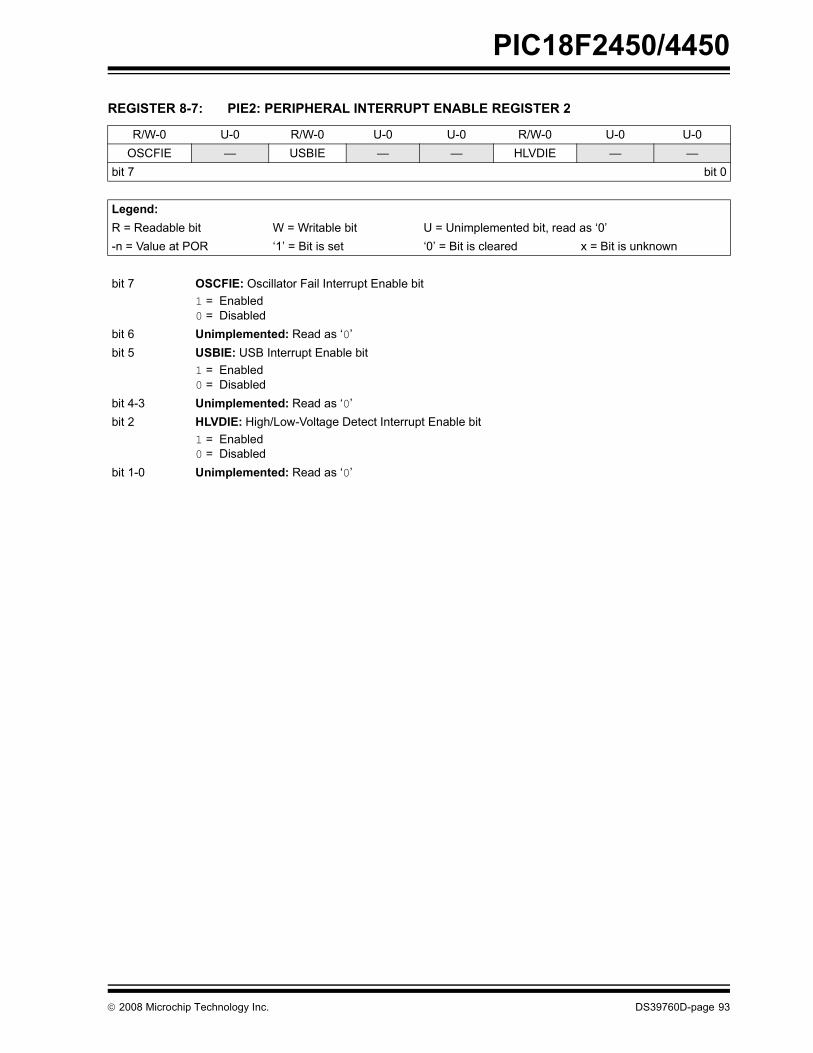
PIC18F2450/4450
© 2008 Microchip Technology Inc. DS39760D-page 93
REGISTER 8-7: PIE2: PERIPHERAL INTERRUPT ENABLE REGISTER 2
R/W-0 U-0 R/W-0 U-0 U-0 R/W-0 U-0 U-0OSCFIE � USBIE � � HLVDIE � �
bit 7 bit 0
Legend:R = Readable bit W = Writable bit U = Unimplemented bit, read as �0�-n = Value at POR �1� = Bit is set �0� = Bit is cleared x = Bit is unknown
bit 7 OSCFIE: Oscillator Fail Interrupt Enable bit1 = Enabled0 = Disabled
bit 6 Unimplemented: Read as �0� bit 5 USBIE: USB Interrupt Enable bit
1 = Enabled0 = Disabled
bit 4-3 Unimplemented: Read as �0� bit 2 HLVDIE: High/Low-Voltage Detect Interrupt Enable bit
1 = Enabled0 = Disabled
bit 1-0 Unimplemented: Read as �0�

PIC18F2450/4450
DS39760D-page 94 © 2008 Microchip Technology Inc.
8.5 IPR RegistersThe IPR registers contain the individual priority bits forthe peripheral interrupts. Due to the number ofperipheral interrupt sources, there are two PeripheralInterrupt Priority registers (IPR1 and IPR2). Using thepriority bits requires that the Interrupt Priority Enable(IPEN) bit be set.
REGISTER 8-8: IPR1: PERIPHERAL INTERRUPT PRIORITY REGISTER 1
U-0 R/W-1 R/W-1 R/W-1 U-0 R/W-1 R/W-1 R/W-1� ADIP RCIP TXIP � CCP1IP TMR2IP TMR1IP
bit 7 bit 0
Legend:R = Readable bit W = Writable bit U = Unimplemented bit, read as �0�-n = Value at POR �1� = Bit is set �0� = Bit is cleared x = Bit is unknown
bit 7 Unimplemented: Read as �0� bit 6 ADIP: A/D Converter Interrupt Priority bit
1 = High priority 0 = Low priority
bit 5 RCIP: EUSART Receive Interrupt Priority bit 1 = High priority 0 = Low priority
bit 4 TXIP: EUSART Transmit Interrupt Priority bit
1 = High priority 0 = Low priority
bit 3 Unimplemented: Read as �0� bit 2 CCP1IP: CCP1 Interrupt Priority bit
1 = High priority 0 = Low priority
bit 1 TMR2IP: TMR2 to PR2 Match Interrupt Priority bit 1 = High priority 0 = Low priority
bit 0 TMR1IP: TMR1 Overflow Interrupt Priority bit 1 = High priority 0 = Low priority

PIC18F2450/4450
© 2008 Microchip Technology Inc. DS39760D-page 95
REGISTER 8-9: IPR2: PERIPHERAL INTERRUPT PRIORITY REGISTER 2
R/W-1 U-0 R/W-1 U-0 U-0 R/W-1 U-0 U-0OSCFIP � USBIP � � HLVDIP � �
bit 7 bit 0
Legend:R = Readable bit W = Writable bit U = Unimplemented bit, read as �0�-n = Value at POR �1� = Bit is set �0� = Bit is cleared x = Bit is unknown
bit 7 OSCFIP: Oscillator Fail Interrupt Priority bit1 = High priority0 = Low priority
bit 6 Unimplemented: Read as �0� bit 5 USBIP: USB Interrupt Priority bit
1 = High priority0 = Low priority
bit 4-3 Unimplemented: Read as �0� bit 2 HLVDIP: High/Low-Voltage Detect Interrupt Priority bit
1 = High priority0 = Low priority
bit 1-0 Unimplemented: Read as �0�
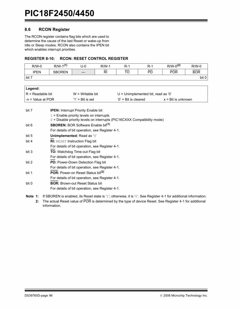
PIC18F2450/4450
DS39760D-page 96 © 2008 Microchip Technology Inc.
8.6 RCON RegisterThe RCON register contains flag bits which are used todetermine the cause of the last Reset or wake-up fromIdle or Sleep modes. RCON also contains the IPEN bitwhich enables interrupt priorities.
REGISTER 8-10: RCON: RESET CONTROL REGISTER
R/W-0 R/W-1(1) U-0 R/W-1 R-1 R-1 R/W-0(2) R/W-0
IPEN SBOREN � RI TO PD POR BORbit 7 bit 0
Legend:R = Readable bit W = Writable bit U = Unimplemented bit, read as �0�-n = Value at POR �1� = Bit is set �0� = Bit is cleared x = Bit is unknown
bit 7 IPEN: Interrupt Priority Enable bit 1 = Enable priority levels on interrupts0 = Disable priority levels on interrupts (PIC16CXXX Compatibility mode)
bit 6 SBOREN: BOR Software Enable bit(1) For details of bit operation, see Register 4-1.
bit 5 Unimplemented: Read as �0�bit 4 RI: RESET Instruction Flag bit
For details of bit operation, see Register 4-1.bit 3 TO: Watchdog Time-out Flag bit
For details of bit operation, see Register 4-1.bit 2 PD: Power-Down Detection Flag bit
For details of bit operation, see Register 4-1.bit 1 POR: Power-on Reset Status bit(2)
For details of bit operation, see Register 4-1.bit 0 BOR: Brown-out Reset Status bit
For details of bit operation, see Register 4-1.
Note 1: If SBOREN is enabled, its Reset state is �1�; otherwise, it is �0�. See Register 4-1 for additional information.2: The actual Reset value of POR is determined by the type of device Reset. See Register 4-1 for additional
information.
PIC18F2450/4450
© 2008 Microchip Technology Inc. DS39760D-page 97
8.7 INTx Pin InterruptsExternal interrupts on the RB0/AN12/INT0, RB1/AN10/INT1and RB2/AN8/INT2/VMO pins are edge-triggered.If the corresponding INTEDGx bit in the INTCON2register is set (= 1), the interrupt is triggered by a risingedge; if the bit is clear, the trigger is on the falling edge.When a valid edge appears on the RBx/INTx pin, thecorresponding flag bit, INTxIF, is set. This interrupt canbe disabled by clearing the corresponding enable bit,INTxIE. Flag bit, INTxIF, must be cleared in software inthe Interrupt Service Routine before re-enabling theinterrupt.
All external interrupts (INT0, INT1 and INT2) can wake-up the processor from the power-managed modes if bit,INTxIE, was set prior to going into the power-managedmodes. If the Global Interrupt Enable bit, GIE, is set, theprocessor will branch to the interrupt vector followingwake-up.
Interrupt priority for INT1 and INT2 is determined bythe value contained in the interrupt priority bits,INT1IP (INTCON3<6>) and INT2IP (INTCON3<7>).There is no priority bit associated with INT0. It isalways a high-priority interrupt source.
8.8 TMR0 InterruptIn 8-bit mode (which is the default), an overflow in theTMR0 register (FFh → 00h) will set flag bit, TMR0IF. In16-bit mode, an overflow in the TMR0H:TMR0Lregister pair (FFFFh → 0000h) will set TMR0IF. Theinterrupt can be enabled/disabled by setting/clearingenable bit, TMR0IE (INTCON<5>). Interrupt priority forTimer0 is determined by the value contained in theinterrupt priority bit, TMR0IP (INTCON2<2>). SeeSection 12.0 �Timer2 Module� for further details onthe Timer0 module.
8.9 PORTB Interrupt-on-ChangeAn input change on PORTB<7:4> sets flag bit, RBIF(INTCON<0>). The interrupt can be enabled/disabledby setting/clearing enable bit, RBIE (INTCON<3>).Interrupt priority for PORTB interrupt-on-change isdetermined by the value contained in the interruptpriority bit, RBIP (INTCON2<0>).
8.10 Context Saving During InterruptsDuring interrupts, the return PC address is saved onthe stack. Additionally, the WREG, STATUS and BSRregisters are saved on the Fast Return Stack. If a fastreturn from interrupt is not used (see Section 5.3�Data Memory Organization�), the user may need tosave the WREG, STATUS and BSR registers on entryto the Interrupt Service Routine. Depending on theuser�s application, other registers may also need to besaved. Example 8-1 saves and restores the WREG,STATUS and BSR registers during an Interrupt ServiceRoutine.
EXAMPLE 8-1: SAVING STATUS, WREG AND BSR REGISTERS IN RAM MOVWF W_TEMP ; W_TEMP is in virtual bankMOVFF STATUS, STATUS_TEMP ; STATUS_TEMP located anywhereMOVFF BSR, BSR_TEMP ; BSR_TMEP located anywhere;; USER ISR CODE;MOVFF BSR_TEMP, BSR ; Restore BSRMOVF W_TEMP, W ; Restore WREGMOVFF STATUS_TEMP, STATUS ; Restore STATUS

PIC18F2450/4450
DS39760D-page 98 © 2008 Microchip Technology Inc.
NOTES:
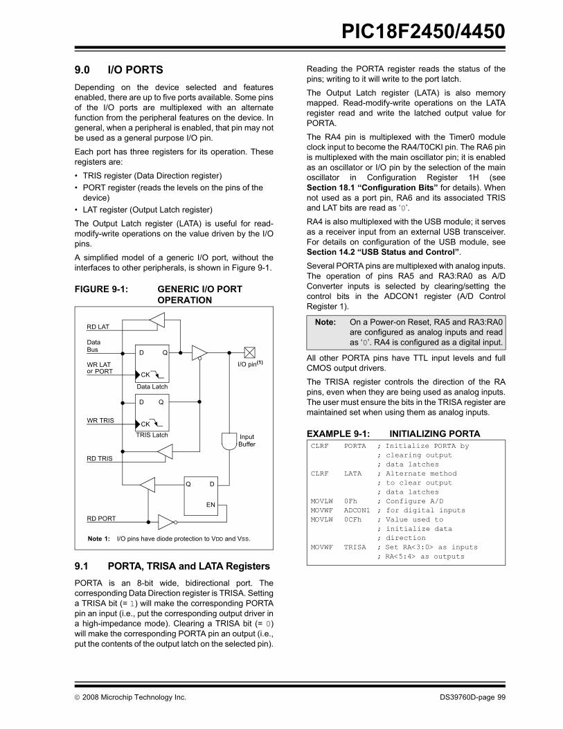
PIC18F2450/4450
© 2008 Microchip Technology Inc. DS39760D-page 99
9.0 I/O PORTSDepending on the device selected and featuresenabled, there are up to five ports available. Some pinsof the I/O ports are multiplexed with an alternatefunction from the peripheral features on the device. Ingeneral, when a peripheral is enabled, that pin may notbe used as a general purpose I/O pin.
Each port has three registers for its operation. Theseregisters are:
� TRIS register (Data Direction register)� PORT register (reads the levels on the pins of the
device)� LAT register (Output Latch register)
The Output Latch register (LATA) is useful for read-modify-write operations on the value driven by the I/Opins.
A simplified model of a generic I/O port, without theinterfaces to other peripherals, is shown in Figure 9-1.
FIGURE 9-1: GENERIC I/O PORT OPERATION
9.1 PORTA, TRISA and LATA RegistersPORTA is an 8-bit wide, bidirectional port. Thecorresponding Data Direction register is TRISA. Settinga TRISA bit (= 1) will make the corresponding PORTApin an input (i.e., put the corresponding output driver ina high-impedance mode). Clearing a TRISA bit (= 0)will make the corresponding PORTA pin an output (i.e.,put the contents of the output latch on the selected pin).
Reading the PORTA register reads the status of thepins; writing to it will write to the port latch.
The Output Latch register (LATA) is also memorymapped. Read-modify-write operations on the LATAregister read and write the latched output value forPORTA.
The RA4 pin is multiplexed with the Timer0 moduleclock input to become the RA4/T0CKI pin. The RA6 pinis multiplexed with the main oscillator pin; it is enabledas an oscillator or I/O pin by the selection of the mainoscillator in Configuration Register 1H (seeSection 18.1 �Configuration Bits� for details). Whennot used as a port pin, RA6 and its associated TRISand LAT bits are read as �0�.
RA4 is also multiplexed with the USB module; it servesas a receiver input from an external USB transceiver.For details on configuration of the USB module, seeSection 14.2 �USB Status and Control�.
Several PORTA pins are multiplexed with analog inputs.The operation of pins RA5 and RA3:RA0 as A/DConverter inputs is selected by clearing/setting thecontrol bits in the ADCON1 register (A/D ControlRegister 1).
All other PORTA pins have TTL input levels and fullCMOS output drivers.
The TRISA register controls the direction of the RApins, even when they are being used as analog inputs.The user must ensure the bits in the TRISA register aremaintained set when using them as analog inputs.
EXAMPLE 9-1: INITIALIZING PORTA
DataBus
WR LAT
WR TRIS
RD PORT
Data Latch
TRIS Latch
RD TRIS
InputBuffer
I/O pin(1)
QD
CK
QD
CK
EN
Q D
EN
RD LAT
or PORT
Note 1: I/O pins have diode protection to VDD and VSS.
Note: On a Power-on Reset, RA5 and RA3:RA0are configured as analog inputs and readas �0�. RA4 is configured as a digital input.
CLRF PORTA ; Initialize PORTA by; clearing output; data latches
CLRF LATA ; Alternate method; to clear output; data latches
MOVLW 0Fh ; Configure A/D MOVWF ADCON1 ; for digital inputsMOVLW 0CFh ; Value used to
; initialize data ; direction
MOVWF TRISA ; Set RA<3:0> as inputs; RA<5:4> as outputs

PIC18F2450/4450
DS39760D-page 100 © 2008 Microchip Technology Inc.
TABLE 9-1: PORTA I/O SUMMARY
TABLE 9-2: SUMMARY OF REGISTERS ASSOCIATED WITH PORTA
Pin Function TRIS Setting I/O I/O Type Description
RA0/AN0 RA0 0 OUT DIG LATA<0> data output; not affected by analog input.1 IN TTL PORTA<0> data input; disabled when analog input enabled.
AN0 1 IN ANA A/D input channel 0. Default configuration on POR; does not affect digital output.
RA1/AN1 RA1 0 OUT DIG LATA<1> data output; not affected by analog input.1 IN TTL PORTA<1> data input; reads �0� on POR.
AN1 1 IN ANA A/D input channel 1. Default configuration on POR; does not affect digital output.
RA2/AN2/VREF-
RA2 0 OUT DIG LATA<2> data output; not affected by analog input.1 IN TTL PORTA<2> data input. Disabled when analog functions enabled.
AN2 1 IN ANA A/D input channel 2. Default configuration on POR; not affected by analog output.
VREF- 1 IN ANA A/D voltage reference low input.RA3/AN3/VREF+
RA3 0 OUT DIG LATA<3> data output; not affected by analog input.1 IN TTL PORTA<3> data input; disabled when analog input enabled.
AN3 1 IN ANA A/D input channel 3. Default configuration on POR.VREF+ 1 IN ANA A/D voltage reference high input.
RA4/T0CKI/RCV
RA4 0 OUT DIG LATA<4> data output; not affected by analog input.1 IN ST PORTA<4> data input; disabled when analog input enabled.
T0CKI 1 IN ST Timer0 clock input.RCV x IN TTL External USB transceiver RCV input.
RA5/AN4/HLVDIN
RA5 0 OUT DIG LATA<5> data output; not affected by analog input.1 IN TTL PORTA<5> data input; disabled when analog input enabled.
AN4 1 IN ANA A/D input channel 4. Default configuration on POR.HLVDIN 1 IN ANA High/Low-Voltage Detect external trip point input.
OSC2/CLKO/RA6
OSC2 x OUT ANA Main oscillator feedback output connection (all XT and HS modes).CLKO x OUT DIG System cycle clock output (FOSC/4); available in EC, ECPLL and
INTCKO modes.RA6 0 OUT DIG LATA<6> data output. Available only in ECIO, ECPIO and INTIO
modes; otherwise, reads as �0�.1 IN TTL PORTA<6> data input. Available only in ECIO, ECPIO and INTIO
modes; otherwise, reads as �0�.Legend: OUT = Output, IN = Input, ANA = Analog Signal, DIG = Digital Output, ST = Schmitt Buffer Input,
TTL = TTL Buffer Input, x = Don�t care (TRIS bit does not affect port direction or is overridden for this option)
Name Bit 7 Bit 6 Bit 5 Bit 4 Bit 3 Bit 2 Bit 1 Bit 0Reset Values
on Page:
PORTA � RA6(1) RA5 RA4 RA3 RA2 RA1 RA0 51LATA � LATA6(1) LATA5 LATA4 LATA3 LATA2 LATA1 LATA0 51TRISA � TRISA6(1) TRISA5 TRISA4 TRISA3 TRISA2 TRISA1 TRISA0 51ADCON1 � � VCFG1 VCFG0 PCFG3 PCFG2 PCFG1 PCFG0 50UCON � PPBRST SE0 PKTDIS USBEN RESUME SUSPND � 52Legend: � = unimplemented, read as �0�. Shaded cells are not used by PORTA.Note 1: RA6 and its associated latch and data direction bits are enabled as I/O pins based on oscillator
configuration; otherwise, they are read as �0�.

PIC18F2450/4450
© 2008 Microchip Technology Inc. DS39760D-page 101
9.2 PORTB, TRISB and LATB Registers
PORTB is an 8-bit wide, bidirectional port. Thecorresponding Data Direction register is TRISB. Settinga TRISB bit (= 1) will make the corresponding PORTBpin an input (i.e., put the corresponding output driver ina high-impedance mode). Clearing a TRISB bit (= 0)will make the corresponding PORTB pin an output (i.e.,put the contents of the output latch on the selected pin).
The Output Latch register (LATB) is also memorymapped. Read-modify-write operations on the LATBregister read and write the latched output value forPORTB.
Each of the PORTB pins has a weak internal pull-up. Asingle control bit can turn on all the pull-ups. This isperformed by clearing bit, RBPU (INTCON2<7>). Theweak pull-up is automatically turned off when the portpin is configured as an output. The pull-ups aredisabled on a Power-on Reset.
Four of the PORTB pins (RB7:RB4) have an interrupt-on-change feature. Only pins configured as inputs cancause this interrupt to occur. Any RB7:RB4 pinconfigured as an output is excluded from the interrupt-on-change comparison. The pins are compared withthe old value latched on the last read of PORTB. The�mismatch� outputs of RB7:RB4 are ORed together togenerate the RB Port Change Interrupt with Flag bit,RBIF (INTCON<0>).
The interrupt-on-change can be used to wake thedevice from Sleep. The user, in the Interrupt ServiceRoutine, can clear the interrupt in the following manner:
a) Any read or write of PORTB (except with theMOVFF (ANY), PORTB instruction). This willend the mismatch condition.
b) Wait one or more instruction cycles.c) Clear flag bit, RBIF.
A mismatch condition will continue to set flag bit, RBIF.Reading PORTB will end the mismatch condition andallow flag bit, RBIF, to be cleared.
The interrupt-on-change feature is recommended forwake-up on key depression operation and operationswhere PORTB is only used for the interrupt-on-changefeature. Polling of PORTB is not recommended whileusing the interrupt-on-change feature.
Pins, RB2 and RB3, are multiplexed with the USBperipheral and serve as the differential signal outputsfor an external USB transceiver (TRIS configuration).Refer to Section 14.2.2.2 �External Transceiver� foradditional information on configuring the USB modulefor operation with an external transceiver.
EXAMPLE 9-2: INITIALIZING PORTB
Note: On a Power-on Reset, RB4:RB0 areconfigured as analog inputs by default andread as �0�; RB7:RB5 are configured asdigital inputs.
By programming the Configuration bit,PBADEN (CONFIG3H<1>), RB4:RB0 willalternatively be configured as digital inputson POR.
CLRF PORTB ; Initialize PORTB by; clearing output; data latches
CLRF LATB ; Alternate method; to clear output; data latches
MOVLW 0Eh ; Set RB<4:0> asMOVWF ADCON1 ; digital I/O pins
; (required if config bit; PBADEN is set)
MOVLW 0CFh ; Value used to; initialize data ; direction
MOVWF TRISB ; Set RB<3:0> as inputs; RB<5:4> as outputs; RB<7:6> as inputs
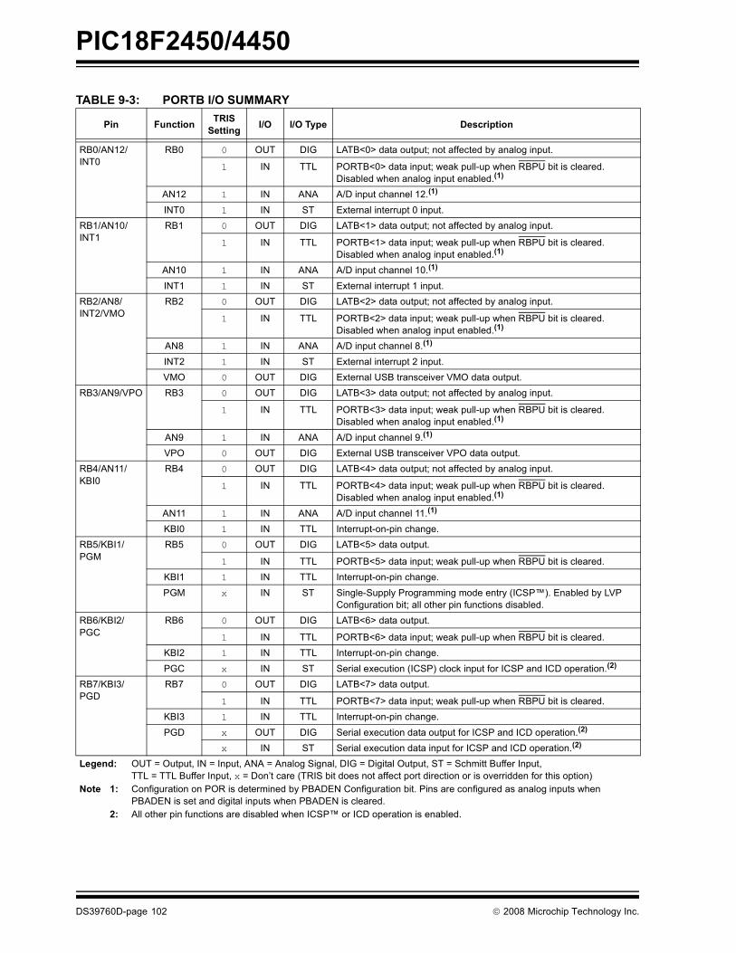
PIC18F2450/4450
DS39760D-page 102 © 2008 Microchip Technology Inc.
TABLE 9-3: PORTB I/O SUMMARY
Pin Function TRIS Setting I/O I/O Type Description
RB0/AN12/INT0
RB0 0 OUT DIG LATB<0> data output; not affected by analog input.
1 IN TTL PORTB<0> data input; weak pull-up when RBPU bit is cleared. Disabled when analog input enabled.(1)
AN12 1 IN ANA A/D input channel 12.(1)
INT0 1 IN ST External interrupt 0 input.RB1/AN10/INT1
RB1 0 OUT DIG LATB<1> data output; not affected by analog input.
1 IN TTL PORTB<1> data input; weak pull-up when RBPU bit is cleared. Disabled when analog input enabled.(1)
AN10 1 IN ANA A/D input channel 10.(1)
INT1 1 IN ST External interrupt 1 input.RB2/AN8/INT2/VMO
RB2 0 OUT DIG LATB<2> data output; not affected by analog input.
1 IN TTL PORTB<2> data input; weak pull-up when RBPU bit is cleared. Disabled when analog input enabled.(1)
AN8 1 IN ANA A/D input channel 8.(1)
INT2 1 IN ST External interrupt 2 input.VMO 0 OUT DIG External USB transceiver VMO data output.
RB3/AN9/VPO RB3 0 OUT DIG LATB<3> data output; not affected by analog input.
1 IN TTL PORTB<3> data input; weak pull-up when RBPU bit is cleared. Disabled when analog input enabled.(1)
AN9 1 IN ANA A/D input channel 9.(1)
VPO 0 OUT DIG External USB transceiver VPO data output.RB4/AN11/KBI0
RB4 0 OUT DIG LATB<4> data output; not affected by analog input.
1 IN TTL PORTB<4> data input; weak pull-up when RBPU bit is cleared. Disabled when analog input enabled.(1)
AN11 1 IN ANA A/D input channel 11.(1)
KBI0 1 IN TTL Interrupt-on-pin change.RB5/KBI1/PGM
RB5 0 OUT DIG LATB<5> data output.
1 IN TTL PORTB<5> data input; weak pull-up when RBPU bit is cleared.KBI1 1 IN TTL Interrupt-on-pin change.PGM x IN ST Single-Supply Programming mode entry (ICSP�). Enabled by LVP
Configuration bit; all other pin functions disabled.RB6/KBI2/PGC
RB6 0 OUT DIG LATB<6> data output.
1 IN TTL PORTB<6> data input; weak pull-up when RBPU bit is cleared.KBI2 1 IN TTL Interrupt-on-pin change.PGC x IN ST Serial execution (ICSP) clock input for ICSP and ICD operation.(2)
RB7/KBI3/PGD
RB7 0 OUT DIG LATB<7> data output.
1 IN TTL PORTB<7> data input; weak pull-up when RBPU bit is cleared.KBI3 1 IN TTL Interrupt-on-pin change.PGD x OUT DIG Serial execution data output for ICSP and ICD operation.(2)
x IN ST Serial execution data input for ICSP and ICD operation.(2)
Legend: OUT = Output, IN = Input, ANA = Analog Signal, DIG = Digital Output, ST = Schmitt Buffer Input, TTL = TTL Buffer Input, x = Don�t care (TRIS bit does not affect port direction or is overridden for this option)
Note 1: Configuration on POR is determined by PBADEN Configuration bit. Pins are configured as analog inputs when PBADEN is set and digital inputs when PBADEN is cleared.
2: All other pin functions are disabled when ICSP� or ICD operation is enabled.
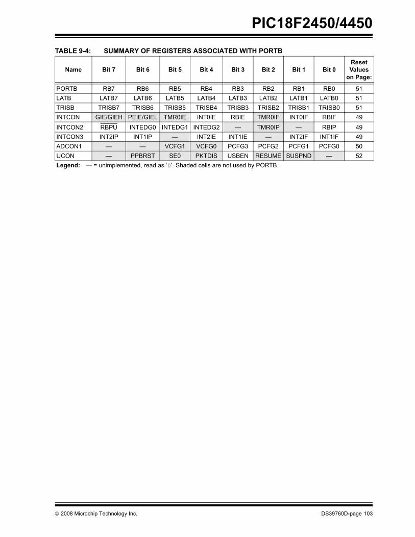
PIC18F2450/4450
© 2008 Microchip Technology Inc. DS39760D-page 103
TABLE 9-4: SUMMARY OF REGISTERS ASSOCIATED WITH PORTB
Name Bit 7 Bit 6 Bit 5 Bit 4 Bit 3 Bit 2 Bit 1 Bit 0Reset Values
on Page:
PORTB RB7 RB6 RB5 RB4 RB3 RB2 RB1 RB0 51LATB LATB7 LATB6 LATB5 LATB4 LATB3 LATB2 LATB1 LATB0 51TRISB TRISB7 TRISB6 TRISB5 TRISB4 TRISB3 TRISB2 TRISB1 TRISB0 51INTCON GIE/GIEH PEIE/GIEL TMR0IE INT0IE RBIE TMR0IF INT0IF RBIF 49
INTCON2 RBPU INTEDG0 INTEDG1 INTEDG2 � TMR0IP � RBIP 49INTCON3 INT2IP INT1IP � INT2IE INT1IE � INT2IF INT1IF 49ADCON1 � � VCFG1 VCFG0 PCFG3 PCFG2 PCFG1 PCFG0 50UCON � PPBRST SE0 PKTDIS USBEN RESUME SUSPND � 52Legend: � = unimplemented, read as �0�. Shaded cells are not used by PORTB.

PIC18F2450/4450
DS39760D-page 104 © 2008 Microchip Technology Inc.
9.3 PORTC, TRISC and LATC Registers
PORTC is a 7-bit wide, bidirectional port. Thecorresponding Data Direction register is TRISC.Setting a TRISC bit (= 1) will make the correspondingPORTC pin an input (i.e., put the corresponding outputdriver in a high-impedance mode). Clearing a TRISCbit (= 0) will make the corresponding PORTC pin anoutput (i.e., put the contents of the output latch on theselected pin).
In PIC18F2450/4450 devices, the RC3 pin is notimplemented.
The Output Latch register (LATC) is also memorymapped. Read-modify-write operations on the LATCregister read and write the latched output value forPORTC.
PORTC is primarily multiplexed with serialcommunication modules, including the EUSART andthe USB module (Table 9-5). Except for RC4 and RC5,PORTC uses Schmitt Trigger input buffers.
Pins RC4 and RC5 are multiplexed with the USBmodule. Depending on the configuration of the module,they can serve as the differential data lines for the on-chip USB transceiver, or the data inputs from anexternal USB transceiver. Both RC4 and RC5 haveTTL input buffers instead of the Schmitt Trigger bufferson the other pins.
Unlike other PORTC pins, RC4 and RC5 do not haveTRISC bits associated with them. As digital ports, theycan only function as digital inputs. When configured forUSB operation, the data direction is determined by theconfiguration and status of the USB module at a giventime. If an external transceiver is used, RC4 and RC5always function as inputs from the transceiver. If theon-chip transceiver is used, the data direction isdetermined by the operation being performed by themodule at that time.
When the external transceiver is enabled, RC2 alsoserves as the output enable control to the transceiver.Additional information on configuring USB options isprovided in Section 14.2.2.2 �External Transceiver�.
When enabling peripheral functions on PORTC pinsother than RC4 and RC5, care should be taken indefining the TRIS bits. Some peripherals override theTRIS bit to make a pin an output, while otherperipherals override the TRIS bit to make a pin aninput. The user should refer to the correspondingperipheral section for the correct TRIS bit settings.
The contents of the TRISC register are affected byperipheral overrides. Reading TRISC always returnsthe current contents, even though a peripheral devicemay be overriding one or more of the pins.
EXAMPLE 9-3: INITIALIZING PORTC
Note: On a Power-on Reset, these pins, exceptRC4 and RC5, are configured as digitalinputs. To use pins RC4 and RC5 asdigital inputs, the USB module must bedisabled (UCON<3> = 0) and the on-chipUSB transceiver must be disabled(UCFG<3> = 1).
CLRF PORTC ; Initialize PORTC by; clearing output; data latches
CLRF LATC ; Alternate method; to clear output; data latches
MOVLW 07h ; Value used to ; initialize data ; direction
MOVWF TRISC ; RC<5:0> as outputs; RC<7:6> as inputs

PIC18F2450/4450
© 2008 Microchip Technology Inc. DS39760D-page 105
TABLE 9-5: PORTC I/O SUMMARY
Pin Function TRIS Setting I/O I/O Type Description
RC0/T1OSO/T1CKI
RC0 0 OUT DIG LATC<0> data output. 1 IN ST PORTC<0> data input.
T1OSO x OUT ANA Timer1 oscillator output; enabled when Timer1 oscillator enabled. Disables digital I/O.
T1CKI 1 IN ST Timer1 counter input.RC1/T1OSI/UOE
RC1 0 OUT DIG LATC<1> data output. 1 IN ST PORTC<1> data input.
T1OSI x IN ANA Timer1 oscillator input; enabled when Timer1 oscillator enabled. Disables digital I/O.
UOE 0 OUT DIG External USB transceiver OE output.RC2/CCP1 RC2 0 OUT DIG LATC<2> data output.
1 IN ST PORTC<2> data input.CCP1 0 OUT DIG CCP1 Compare and PWM output; takes priority over port data.
1 IN ST CCP1 Capture input.RC4/D-/VM RC4 �(1) IN TTL PORTC<4> data input; disabled when USB module or on-chip
transceiver is enabled.D- �(1) OUT XCVR USB bus differential minus line output (internal transceiver).
�(1) IN XCVR USB bus differential minus line input (internal transceiver).VM �(1) IN TTL External USB transceiver VM input.
RC5/D+/VP RC5 �(1) IN TTL PORTC<5> data input; disabled when USB module or on-chip transceiver is enabled.
D+ �(1) OUT XCVR USB bus differential plus line output (internal transceiver).�(1) IN XCVR USB bus differential plus line input (internal transceiver).
VP �(1) IN TTL External USB transceiver VP input.RC6/TX/CK RC6 0 OUT DIG LATC<6> data output.
1 IN ST PORTC<6> data input.TX 0 OUT DIG Asynchronous serial transmit data output (EUSART module); takes
priority over port data. User must configure as output.CK 0 OUT DIG Synchronous serial clock output (EUSART module); takes priority
over port data.1 IN ST Synchronous serial clock input (EUSART module).
RC7/RX/DT RC7 0 OUT DIG LATC<7> data output.1 IN ST PORTC<7> data input.
RX 1 IN ST Asynchronous serial receive data input (EUSART module).DT 1 OUT DIG Synchronous serial data output (EUSART module).
1 IN ST Synchronous serial data input (EUSART module). User must configure as an input.
Legend: OUT = Output, IN = Input, ANA = Analog Signal, DIG = Digital Output, ST = Schmitt Buffer Input, TTL = TTL Buffer Input, XCVR = USB Transceiver, x = Don�t care (TRIS bit does not affect port direction or is overridden for this option)
Note 1: RC4 and RC5 do not have corresponding TRISC bits. In Port mode, these pins are input only. USB data direction is determined by the USB configuration.

PIC18F2450/4450
DS39760D-page 106 © 2008 Microchip Technology Inc.
TABLE 9-6: SUMMARY OF REGISTERS ASSOCIATED WITH PORTC
Name Bit 7 Bit 6 Bit 5 Bit 4 Bit 3 Bit 2 Bit 1 Bit 0Reset Values
on Page:
PORTC RC7 RC6 RC5(1) RC4(1) � RC2 RC1 RC0 51LATC LATC7 LATC6 � � � LATC2 LATC1 LATC0 51TRISC TRISC7 TRISC6 � � � TRISC2 TRISC1 TRISC0 51UCON � PPBRST SE0 PKTDIS USBEN RESUME SUSPND � 52Legend: � = unimplemented, read as �0�. Shaded cells are not used by PORTC.Note 1: RC5 and RC4 are only available as port pins when the USB module is disabled (UCON<3> = 0).

PIC18F2450/4450
© 2008 Microchip Technology Inc. DS39760D-page 107
9.4 PORTD, TRISD and LATD Registers
PORTD is an 8-bit wide, bidirectional port. Thecorresponding Data Direction register is TRISD.Setting a TRISD bit (= 1) will make the correspondingPORTD pin an input (i.e., put the corresponding outputdriver in a high-impedance mode). Clearing a TRISDbit (= 0) will make the corresponding PORTD pin anoutput (i.e., put the contents of the output latch on theselected pin).
The Output Latch register (LATD) is also memorymapped. Read-modify-write operations on the LATDregister read and write the latched output value forPORTD.
All pins on PORTD are implemented with SchmittTrigger input buffers. Each pin is individuallyconfigurable as an input or output.
EXAMPLE 9-4: INITIALIZING PORTD
Note: PORTD is only available on 40/44-pindevices.
Note: On a Power-on Reset, these pins areconfigured as digital inputs.
CLRF PORTD ; Initialize PORTD by ; clearing output ; data latchesCLRF LATD ; Alternate method
; to clear output; data latches
MOVLW 0CFh ; Value used to ; initialize data ; direction
MOVWF TRISD ; Set RD<3:0> as inputs; RD<5:4> as outputs; RD<7:6> as inputs
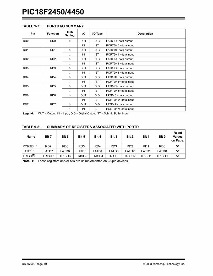
PIC18F2450/4450
DS39760D-page 108 © 2008 Microchip Technology Inc.
TABLE 9-7: PORTD I/O SUMMARY
TABLE 9-8: SUMMARY OF REGISTERS ASSOCIATED WITH PORTD
Pin Function TRIS Setting I/O I/O Type Description
RD0 RD0 0 OUT DIG LATD<0> data output.1 IN ST PORTD<0> data input.
RD1 RD1 0 OUT DIG LATD<1> data output.1 IN ST PORTD<1> data input.
RD2 RD2 0 OUT DIG LATD<2> data output.1 IN ST PORTD<2> data input.
RD3 RD3 0 OUT DIG LATD<3> data output.1 IN ST PORTD<3> data input.
RD4 RD4 0 OUT DIG LATD<4> data output.1 IN ST PORTD<4> data input.
RD5 RD5 0 OUT DIG LATD<5> data output1 IN ST PORTD<5> data input
RD6 RD6 0 OUT DIG LATD<6> data output.1 IN ST PORTD<6> data input.
RD7 RD7 0 OUT DIG LATD<7> data output.1 IN ST PORTD<7> data input.
Legend: OUT = Output, IN = Input, DIG = Digital Output, ST = Schmitt Buffer Input
Name Bit 7 Bit 6 Bit 5 Bit 4 Bit 3 Bit 2 Bit 1 Bit 0Reset Values
on Page:
PORTD(1) RD7 RD6 RD5 RD4 RD3 RD2 RD1 RD0 51LATD(1) LATD7 LATD6 LATD5 LATD4 LATD3 LATD2 LATD1 LATD0 51TRISD(1) TRISD7 TRISD6 TRISD5 TRISD4 TRISD3 TRISD2 TRISD1 TRISD0 51Note 1: These registers and/or bits are unimplemented on 28-pin devices.
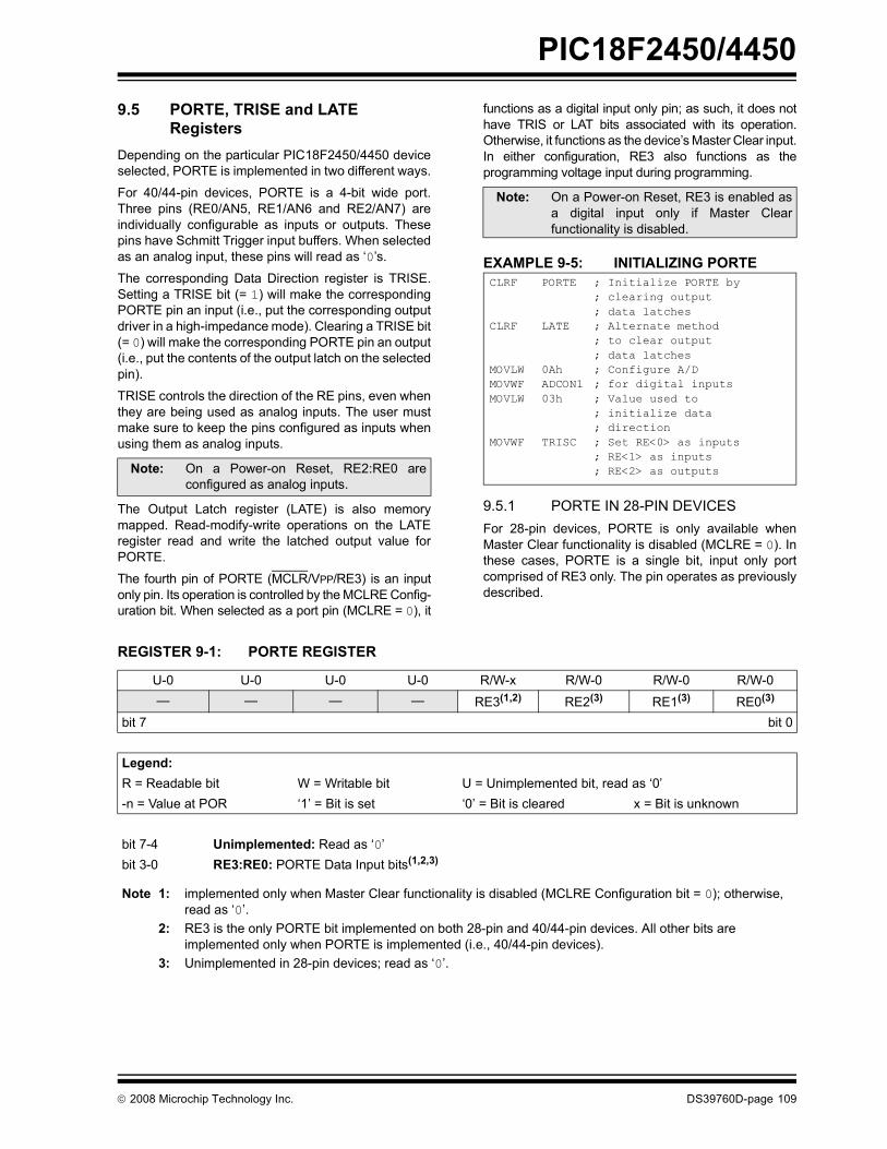
PIC18F2450/4450
© 2008 Microchip Technology Inc. DS39760D-page 109
9.5 PORTE, TRISE and LATE Registers
Depending on the particular PIC18F2450/4450 deviceselected, PORTE is implemented in two different ways.
For 40/44-pin devices, PORTE is a 4-bit wide port.Three pins (RE0/AN5, RE1/AN6 and RE2/AN7) areindividually configurable as inputs or outputs. Thesepins have Schmitt Trigger input buffers. When selectedas an analog input, these pins will read as �0�s.
The corresponding Data Direction register is TRISE.Setting a TRISE bit (= 1) will make the correspondingPORTE pin an input (i.e., put the corresponding outputdriver in a high-impedance mode). Clearing a TRISE bit(= 0) will make the corresponding PORTE pin an output(i.e., put the contents of the output latch on the selectedpin).
TRISE controls the direction of the RE pins, even whenthey are being used as analog inputs. The user mustmake sure to keep the pins configured as inputs whenusing them as analog inputs.
The Output Latch register (LATE) is also memorymapped. Read-modify-write operations on the LATEregister read and write the latched output value forPORTE.
The fourth pin of PORTE (MCLR/VPP/RE3) is an inputonly pin. Its operation is controlled by the MCLRE Config-uration bit. When selected as a port pin (MCLRE = 0), it
functions as a digital input only pin; as such, it does nothave TRIS or LAT bits associated with its operation.Otherwise, it functions as the device�s Master Clear input.In either configuration, RE3 also functions as theprogramming voltage input during programming.
EXAMPLE 9-5: INITIALIZING PORTE
9.5.1 PORTE IN 28-PIN DEVICESFor 28-pin devices, PORTE is only available whenMaster Clear functionality is disabled (MCLRE = 0). Inthese cases, PORTE is a single bit, input only portcomprised of RE3 only. The pin operates as previouslydescribed.
Note: On a Power-on Reset, RE2:RE0 areconfigured as analog inputs.
Note: On a Power-on Reset, RE3 is enabled asa digital input only if Master Clearfunctionality is disabled.
CLRF PORTE ; Initialize PORTE by; clearing output; data latches
CLRF LATE ; Alternate method; to clear output; data latches
MOVLW 0Ah ; Configure A/D MOVWF ADCON1 ; for digital inputsMOVLW 03h ; Value used to
; initialize data ; direction
MOVWF TRISC ; Set RE<0> as inputs; RE<1> as inputs; RE<2> as outputs
REGISTER 9-1: PORTE REGISTER
U-0 U-0 U-0 U-0 R/W-x R/W-0 R/W-0 R/W-0� � � � RE3(1,2) RE2(3) RE1(3) RE0(3)
bit 7 bit 0
Legend:R = Readable bit W = Writable bit U = Unimplemented bit, read as �0�-n = Value at POR �1� = Bit is set �0� = Bit is cleared x = Bit is unknown
bit 7-4 Unimplemented: Read as �0�bit 3-0 RE3:RE0: PORTE Data Input bits(1,2,3)
Note 1: implemented only when Master Clear functionality is disabled (MCLRE Configuration bit = 0); otherwise, read as �0�.
2: RE3 is the only PORTE bit implemented on both 28-pin and 40/44-pin devices. All other bits are implemented only when PORTE is implemented (i.e., 40/44-pin devices).
3: Unimplemented in 28-pin devices; read as �0�.

PIC18F2450/4450
DS39760D-page 110 © 2008 Microchip Technology Inc.
TABLE 9-9: PORTE I/O SUMMARY
TABLE 9-10: SUMMARY OF REGISTERS ASSOCIATED WITH PORTE
Pin Function TRIS Setting I/O I/O Type Description
RE0/AN5 RE0 0 OUT DIG LATE<0> data output; not affected by analog input.1 IN ST PORTE<0> data input; disabled when analog input enabled.
AN5 1 IN ANA A/D input channel 5; default configuration on POR.RE1/AN6 RE1 0 OUT DIG LATE<1> data output; not affected by analog input.
1 IN ST PORTE<1> data input; disabled when analog input enabled.AN6 1 IN ANA A/D input channel 6; default configuration on POR.
RE2/AN7 RE2 0 OUT DIG LATE<2> data output; not affected by analog input.1 IN ST PORTE<2> data input; disabled when analog input enabled.
AN7 1 IN ANA A/D input channel 7; default configuration on POR.
MCLR/VPP/RE3
MCLR �(1) IN ST External Master Clear input; enabled when MCLRE Configuration bit is set.
VPP � (1) IN ANA High-voltage detection, used for ICSP� mode entry detection. Always available regardless of pin mode.
RE3 � (1) IN ST PORTE<3> data input; enabled when MCLRE Configuration bit is clear.
Legend: OUT = Output, IN = Input, ANA = Analog Signal, DIG = Digital Output, ST = Schmitt Buffer Input.Note 1: RE3 does not have a corresponding TRISE<3> bit. This pin is always an input regardless of mode.
Name Bit 7 Bit 6 Bit 5 Bit 4 Bit 3 Bit 2 Bit 1 Bit 0Reset Values
on Page:
PORTE � � � � RE3(1,2) RE2(3) RE1(3) RE0(3) 51LATE(3) � � � � � LATE2 LATE1 LATE0 51TRISE(3) � � � � � TRISE2 TRISE1 TRISE0 51ADCON1 � � VCFG1 VCFG0 PCFG3 PCFG2 PCFG1 PCFG0 50Legend: � = unimplemented, read as �0�Note 1: Implemented only when Master Clear functionality is disabled (MCLRE Configuration bit = 0); otherwise,
read as �0�.2: RE3 is the only PORTE bit implemented on both 28-pin and 40/44-pin devices. All other bits are
implemented only when PORTE is implemented (i.e., 40/44-pin devices).3: These registers and/or bits are unimplemented on 28-pin devices.
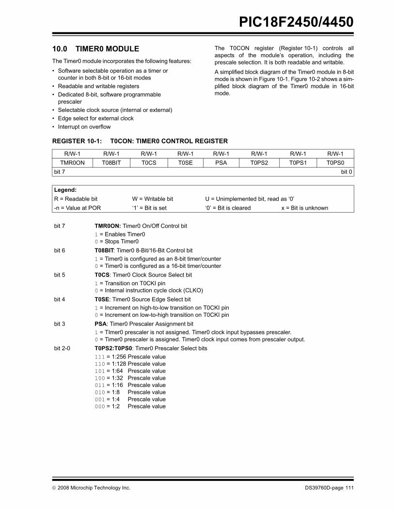
PIC18F2450/4450
© 2008 Microchip Technology Inc. DS39760D-page 111
10.0 TIMER0 MODULEThe Timer0 module incorporates the following features:
� Software selectable operation as a timer or counter in both 8-bit or 16-bit modes
� Readable and writable registers� Dedicated 8-bit, software programmable
prescaler� Selectable clock source (internal or external)� Edge select for external clock� Interrupt on overflow
The T0CON register (Register 10-1) controls allaspects of the module�s operation, including theprescale selection. It is both readable and writable.
A simplified block diagram of the Timer0 module in 8-bitmode is shown in Figure 10-1. Figure 10-2 shows a sim-plified block diagram of the Timer0 module in 16-bitmode.
REGISTER 10-1: T0CON: TIMER0 CONTROL REGISTER
R/W-1 R/W-1 R/W-1 R/W-1 R/W-1 R/W-1 R/W-1 R/W-1TMR0ON T08BIT T0CS T0SE PSA T0PS2 T0PS1 T0PS0
bit 7 bit 0
Legend:R = Readable bit W = Writable bit U = Unimplemented bit, read as �0�-n = Value at POR �1� = Bit is set �0� = Bit is cleared x = Bit is unknown
bit 7 TMR0ON: Timer0 On/Off Control bit 1 = Enables Timer0 0 = Stops Timer0
bit 6 T08BIT: Timer0 8-Bit/16-Bit Control bit 1 = Timer0 is configured as an 8-bit timer/counter 0 = Timer0 is configured as a 16-bit timer/counter
bit 5 T0CS: Timer0 Clock Source Select bit 1 = Transition on T0CKI pin 0 = Internal instruction cycle clock (CLKO)
bit 4 T0SE: Timer0 Source Edge Select bit1 = Increment on high-to-low transition on T0CKI pin 0 = Increment on low-to-high transition on T0CKI pin
bit 3 PSA: Timer0 Prescaler Assignment bit 1 = TImer0 prescaler is not assigned. Timer0 clock input bypasses prescaler. 0 = Timer0 prescaler is assigned. Timer0 clock input comes from prescaler output.
bit 2-0 T0PS2:T0PS0: Timer0 Prescaler Select bits 111 = 1:256 Prescale value110 = 1:128 Prescale value101 = 1:64 Prescale value100 = 1:32 Prescale value011 = 1:16 Prescale value010 = 1:8 Prescale value001 = 1:4 Prescale value000 = 1:2 Prescale value

PIC18F2450/4450
DS39760D-page 112 © 2008 Microchip Technology Inc.
10.1 Timer0 OperationTimer0 can operate as either a timer or a counter; themode is selected by clearing the T0CS bit(T0CON<5>). In Timer mode, the module incrementson every clock by default unless a different prescalervalue is selected (see Section 10.3 �Prescaler�). Ifthe TMR0 register is written to, the increment isinhibited for the following two instruction cycles. Theuser can work around this by writing an adjusted valueto the TMR0 register.
The Counter mode is selected by setting the T0CS bit(= 1). In Counter mode, Timer0 increments either onevery rising or falling edge of pin RA4/T0CKI. Theincrementing edge is determined by the Timer0 SourceEdge Select bit, T0SE (T0CON<4>); clearing this bitselects the rising edge. Restrictions on the externalclock input are discussed below.
An external clock source can be used to drive Timer0;however, it must meet certain requirements to ensurethat the external clock can be synchronized with the
internal phase clock (TOSC). There is a delay betweensynchronization and the onset of incrementing thetimer/counter.
10.2 Timer0 Reads and Writes in 16-Bit Mode
TMR0H is not the actual high byte of Timer0 in 16-bitmode; it is actually a buffered version of the real highbyte of Timer0, which is not directly readable norwritable (refer to Figure 10-2). TMR0H is updated withthe contents of the high byte of Timer0 during a read ofTMR0L. This provides the ability to read all 16 bits ofTimer0 without having to verify that the read of the highand low byte were valid, due to a rollover betweensuccessive reads of the high and low byte.
Similarly, a write to the high byte of Timer0 must alsotake place through the TMR0H Buffer register. The highbyte is updated with the contents of TMR0H when awrite occurs to TMR0L. This allows all 16 bits of Timer0to be updated at once.
FIGURE 10-1: TIMER0 BLOCK DIAGRAM (8-BIT MODE)
FIGURE 10-2: TIMER0 BLOCK DIAGRAM (16-BIT MODE)
Note: Upon Reset, Timer0 is enabled in 8-bit mode with clock input from T0CKI maximum prescale.
T0CKI pin
T0SE
0
1
1
0
T0CS
FOSC/4
ProgrammablePrescaler
Sync withInternalClocks
TMR0L
(2 TCY Delay)
Internal Data BusPSAT0PS2:T0PS0
Set TMR0IFon Overflow
3 8
8
Note: Upon Reset, Timer0 is enabled in 8-bit mode with clock input from T0CKI maximum prescale.
T0CKI pin
T0SE
0
1
1
0
T0CS
FOSC/4
ProgrammablePrescaler
Sync withInternalClocks
TMR0L
(2 TCY Delay)
Internal Data Bus
8
PSAT0PS2:T0PS0
Set TMR0IFon Overflow
3
TMR0
TMR0H
High Byte
88
8
Read TMR0L
Write TMR0L
8

PIC18F2450/4450
© 2008 Microchip Technology Inc. DS39760D-page 113
10.3 PrescalerAn 8-bit counter is available as a prescaler for the Timer0module. The prescaler is not directly readable or writable;its value is set by the PSA and T0PS2:T0PS0 bits(T0CON<3:0>) which determine the prescalerassignment and prescale ratio.
Clearing the PSA bit assigns the prescaler to theTimer0 module. When it is assigned, prescale valuesfrom 1:2 through 1:256, in power-of-2 increments, areselectable.
When assigned to the Timer0 module, all instructionswriting to the TMR0 register (e.g., CLRF TMR0, MOVWFTMR0, BSF TMR0,etc.) clear the prescaler count.
10.3.1 SWITCHING PRESCALER ASSIGNMENT
The prescaler assignment is fully under softwarecontrol and can be changed �on-the-fly� during programexecution.
10.4 Timer0 InterruptThe TMR0 interrupt is generated when the TMR0register overflows from FFh to 00h in 8-bit mode, orfrom FFFFh to 0000h in 16-bit mode. This overflow setsthe TMR0IF flag bit. The interrupt can be masked byclearing the TMR0IE bit (INTCON<5>). Before re-enabling the interrupt, the TMR0IF bit must be clearedin software by the Interrupt Service Routine.
Since Timer0 is shut down in Sleep mode, the TMR0interrupt cannot awaken the processor from Sleep.
TABLE 10-1: REGISTERS ASSOCIATED WITH TIMER0
Note: Writing to TMR0 when the prescaler isassigned to Timer0 will clear the prescalercount but will not change the prescalerassignment.
Name Bit 7 Bit 6 Bit 5 Bit 4 Bit 3 Bit 2 Bit 1 Bit 0Reset Values
on Page:
TMR0L Timer0 Register Low Byte 50TMR0H Timer0 Register High Byte 50INTCON GIE/GIEH PEIE/GIEL TMR0IE INT0IE RBIE TMR0IF INT0IF RBIF 49T0CON TMR0ON T08BIT T0CS T0SE PSA T0PS2 T0PS1 T0PS0 50TRISA � TRISA6(1) TRISA5 TRISA4 TRISA3 TRISA2 TRISA1 TRISA0 51Legend: � = unimplemented locations, read as �0�. Shaded cells are not used by Timer0.Note 1: RA6 is configured as a port pin based on various primary oscillator modes. When the port pin is disabled,
all of the associated bits read �0�.

PIC18F2450/4450
DS39760D-page 114 © 2008 Microchip Technology Inc.
NOTES:
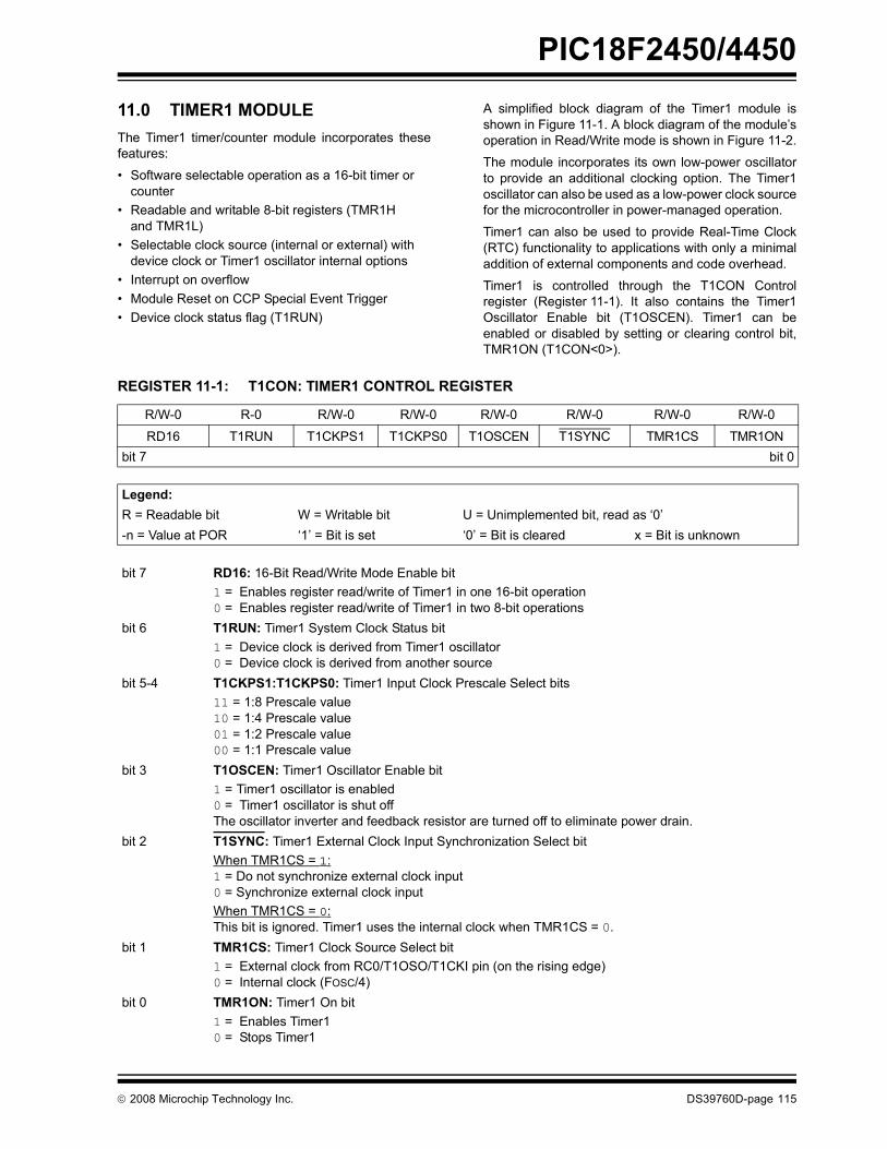
PIC18F2450/4450
© 2008 Microchip Technology Inc. DS39760D-page 115
11.0 TIMER1 MODULEThe Timer1 timer/counter module incorporates thesefeatures:
� Software selectable operation as a 16-bit timer or counter
� Readable and writable 8-bit registers (TMR1H and TMR1L)
� Selectable clock source (internal or external) with device clock or Timer1 oscillator internal options
� Interrupt on overflow� Module Reset on CCP Special Event Trigger� Device clock status flag (T1RUN)
A simplified block diagram of the Timer1 module isshown in Figure 11-1. A block diagram of the module�soperation in Read/Write mode is shown in Figure 11-2.
The module incorporates its own low-power oscillatorto provide an additional clocking option. The Timer1oscillator can also be used as a low-power clock sourcefor the microcontroller in power-managed operation.
Timer1 can also be used to provide Real-Time Clock(RTC) functionality to applications with only a minimaladdition of external components and code overhead.
Timer1 is controlled through the T1CON Controlregister (Register 11-1). It also contains the Timer1Oscillator Enable bit (T1OSCEN). Timer1 can beenabled or disabled by setting or clearing control bit,TMR1ON (T1CON<0>).
REGISTER 11-1: T1CON: TIMER1 CONTROL REGISTER
R/W-0 R-0 R/W-0 R/W-0 R/W-0 R/W-0 R/W-0 R/W-0
RD16 T1RUN T1CKPS1 T1CKPS0 T1OSCEN T1SYNC TMR1CS TMR1ONbit 7 bit 0
Legend:R = Readable bit W = Writable bit U = Unimplemented bit, read as �0�-n = Value at POR �1� = Bit is set �0� = Bit is cleared x = Bit is unknown
bit 7 RD16: 16-Bit Read/Write Mode Enable bit1 = Enables register read/write of Timer1 in one 16-bit operation0 = Enables register read/write of Timer1 in two 8-bit operations
bit 6 T1RUN: Timer1 System Clock Status bit1 = Device clock is derived from Timer1 oscillator0 = Device clock is derived from another source
bit 5-4 T1CKPS1:T1CKPS0: Timer1 Input Clock Prescale Select bits11 = 1:8 Prescale value 10 = 1:4 Prescale value 01 = 1:2 Prescale value 00 = 1:1 Prescale value
bit 3 T1OSCEN: Timer1 Oscillator Enable bit1 = Timer1 oscillator is enabled 0 = Timer1 oscillator is shut off The oscillator inverter and feedback resistor are turned off to eliminate power drain.
bit 2 T1SYNC: Timer1 External Clock Input Synchronization Select bitWhen TMR1CS = 1: 1 = Do not synchronize external clock input 0 = Synchronize external clock inputWhen TMR1CS = 0: This bit is ignored. Timer1 uses the internal clock when TMR1CS = 0.
bit 1 TMR1CS: Timer1 Clock Source Select bit1 = External clock from RC0/T1OSO/T1CKI pin (on the rising edge)0 = Internal clock (FOSC/4)
bit 0 TMR1ON: Timer1 On bit1 = Enables Timer1 0 = Stops Timer1
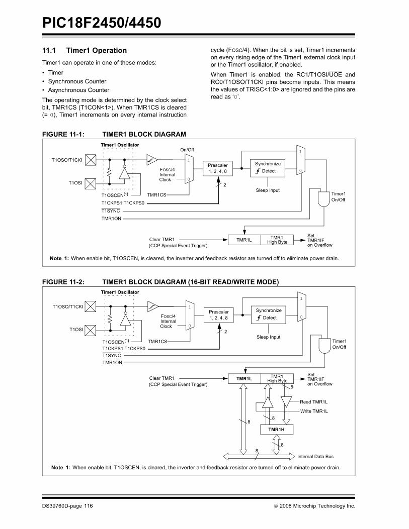
PIC18F2450/4450
DS39760D-page 116 © 2008 Microchip Technology Inc.
11.1 Timer1 OperationTimer1 can operate in one of these modes:
� Timer� Synchronous Counter� Asynchronous Counter
The operating mode is determined by the clock selectbit, TMR1CS (T1CON<1>). When TMR1CS is cleared(= 0), Timer1 increments on every internal instruction
cycle (FOSC/4). When the bit is set, Timer1 incrementson every rising edge of the Timer1 external clock inputor the Timer1 oscillator, if enabled.
When Timer1 is enabled, the RC1/T1OSI/UOE andRC0/T1OSO/T1CKI pins become inputs. This meansthe values of TRISC<1:0> are ignored and the pins areread as �0�.
FIGURE 11-1: TIMER1 BLOCK DIAGRAM
FIGURE 11-2: TIMER1 BLOCK DIAGRAM (16-BIT READ/WRITE MODE)
T1SYNC
TMR1CS
T1CKPS1:T1CKPS0
Sleep InputT1OSCEN(1)
FOSC/4InternalClock
On/Off
Prescaler1, 2, 4, 8
SynchronizeDetect
1
02
T1OSO/T1CKI
T1OSI
1
0
TMR1ON
TMR1LSet TMR1IFon Overflow
TMR1 High ByteClear TMR1
(CCP Special Event Trigger)
Timer1 Oscillator
Note 1: When enable bit, T1OSCEN, is cleared, the inverter and feedback resistor are turned off to eliminate power drain.
On/OffTimer1
T1SYNC
TMR1CST1CKPS1:T1CKPS0
Sleep InputT1OSCEN(1)
FOSC/4InternalClock
Prescaler1, 2, 4, 8
SynchronizeDetect
1
02
T1OSO/T1CKI
T1OSI
Note 1: When enable bit, T1OSCEN, is cleared, the inverter and feedback resistor are turned off to eliminate power drain.
1
0
TMR1L
Internal Data Bus
8
Set TMR1IFon Overflow
TMR1
TMR1H
High Byte
88
8
Read TMR1L
Write TMR1L
8
TMR1ON
Clear TMR1(CCP Special Event Trigger)
Timer1 Oscillator
On/OffTimer1

PIC18F2450/4450
© 2008 Microchip Technology Inc. DS39760D-page 117
11.2 Timer1 16-Bit Read/Write ModeTimer1 can be configured for 16-bit reads and writes(see Figure 11-2). When the RD16 control bit(T1CON<7>) is set, the address for TMR1H is mappedto a buffer register for the high byte of Timer1. A readfrom TMR1L will load the contents of the high byte ofTimer1 into the Timer1 high byte buffer. This providesthe user with the ability to accurately read all 16 bits ofTimer1 without having to determine whether a read ofthe high byte, followed by a read of the low byte, hasbecome invalid due to a rollover between reads.
A write to the high byte of Timer1 must also take placethrough the TMR1H Buffer register. The Timer1 highbyte is updated with the contents of TMR1H when awrite occurs to TMR1L. This allows a user to write all16 bits to both the high and low bytes of Timer1 at once.
The high byte of Timer1 is not directly readable orwritable in this mode. All reads and writes must takeplace through the Timer1 High Byte Buffer register.Writes to TMR1H do not clear the Timer1 prescaler.The prescaler is only cleared on writes to TMR1L.
11.3 Timer1 OscillatorAn on-chip crystal oscillator circuit is incorporatedbetween pins T1OSI (input) and T1OSO (amplifieroutput). It is enabled by setting the Timer1 OscillatorEnable bit, T1OSCEN (T1CON<3>). The oscillator is alow-power circuit rated for 32 kHz crystals. It willcontinue to run during all power-managed modes. Thecircuit for a typical LP oscillator is shown in Figure 11-3.Table 11-1 shows the capacitor selection for the Timer1oscillator.
The user must provide a software time delay to ensureproper start-up of the Timer1 oscillator.
FIGURE 11-3: EXTERNAL COMPONENTS FOR THE TIMER1 LP OSCILLATOR
TABLE 11-1: CAPACITOR SELECTION FOR THE TIMER OSCILLATOR(2,3,4)
11.3.1 USING TIMER1 AS A CLOCK SOURCE
The Timer1 oscillator is also available as a clock sourcein power-managed modes. By setting the clock selectbits, SCS1:SCS0 (OSCCON<1:0>), to �01�, the deviceswitches to SEC_RUN mode. Both the CPU andperipherals are clocked from the Timer1 oscillator. If theIDLEN bit (OSCCON<7>) is cleared and a SLEEPinstruction is executed, the device enters SEC_IDLEmode. Additional details are available in Section 3.0�Power-Managed Modes�.
Whenever the Timer1 oscillator is providing the clocksource, the Timer1 system clock status flag, T1RUN(T1CON<6>), is set. This can be used to determine thecontroller�s current clocking mode. It can also indicatethe clock source being currently used by the Fail-SafeClock Monitor. If the Clock Monitor is enabled and theTimer1 oscillator fails while providing the clock, pollingthe T1RUN bit will indicate whether the clock is beingprovided by the Timer1 oscillator or another source.
11.3.2 LOW-POWER TIMER1 OPTIONThe Timer1 oscillator can operate at two distinct levelsof power consumption based on device configuration.When the LPT1OSC Configuration bit is set, the Timer1oscillator operates in a low-power mode. WhenLPT1OSC is not set, Timer1 operates at a higher powerlevel. Power consumption for a particular mode isrelatively constant, regardless of the device�s operatingmode. The default Timer1 configuration is the higherpower mode.
As the Low-Power Timer1 mode tends to be moresensitive to interference, high noise environments maycause some oscillator instability. The low-power optionis, therefore, best suited for low noise applicationswhere power conservation is an important designconsideration.
Note: See the Notes with Table 11-1 for additionalinformation about capacitor selection.
C1
C2
XTAL
PIC18FXXXXT1OSI
T1OSO
32.768 kHz
33 pF
33 pF
Osc Type Freq C1 C2LP 32 kHz 27 pF(1) 27 pF(1)
Note 1: Microchip suggests these values as astarting point in validating the oscillatorcircuit.
2: Higher capacitance increases the stabilityof the oscillator but also increases thestart-up time.
3: Since each resonator/crystal has its owncharacteristics, the user should consultthe resonator/crystal manufacturer forappropriate values of externalcomponents.
4: Capacitor values are for design guidanceonly.
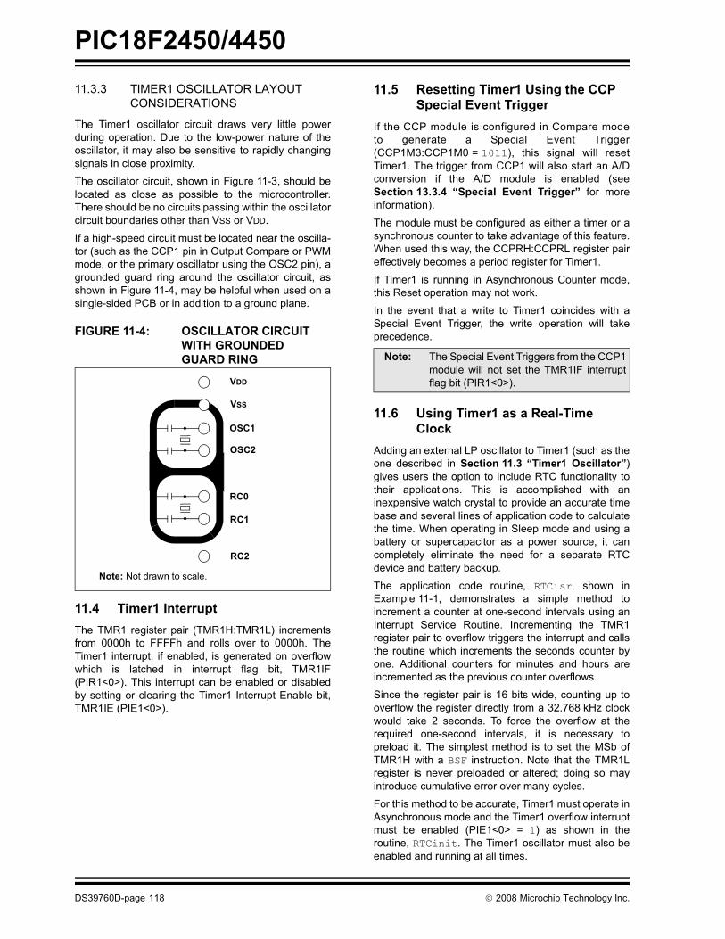
PIC18F2450/4450
DS39760D-page 118 © 2008 Microchip Technology Inc.
11.3.3 TIMER1 OSCILLATOR LAYOUT CONSIDERATIONS
The Timer1 oscillator circuit draws very little powerduring operation. Due to the low-power nature of theoscillator, it may also be sensitive to rapidly changingsignals in close proximity.
The oscillator circuit, shown in Figure 11-3, should belocated as close as possible to the microcontroller.There should be no circuits passing within the oscillatorcircuit boundaries other than VSS or VDD.
If a high-speed circuit must be located near the oscilla-tor (such as the CCP1 pin in Output Compare or PWMmode, or the primary oscillator using the OSC2 pin), agrounded guard ring around the oscillator circuit, asshown in Figure 11-4, may be helpful when used on asingle-sided PCB or in addition to a ground plane.
FIGURE 11-4: OSCILLATOR CIRCUIT WITH GROUNDED GUARD RING
11.4 Timer1 InterruptThe TMR1 register pair (TMR1H:TMR1L) incrementsfrom 0000h to FFFFh and rolls over to 0000h. TheTimer1 interrupt, if enabled, is generated on overflowwhich is latched in interrupt flag bit, TMR1IF(PIR1<0>). This interrupt can be enabled or disabledby setting or clearing the Timer1 Interrupt Enable bit,TMR1IE (PIE1<0>).
11.5 Resetting Timer1 Using the CCP Special Event Trigger
If the CCP module is configured in Compare modeto generate a Special Event Trigger(CCP1M3:CCP1M0 = 1011), this signal will resetTimer1. The trigger from CCP1 will also start an A/Dconversion if the A/D module is enabled (seeSection 13.3.4 �Special Event Trigger� for moreinformation).
The module must be configured as either a timer or asynchronous counter to take advantage of this feature.When used this way, the CCPRH:CCPRL register paireffectively becomes a period register for Timer1.
If Timer1 is running in Asynchronous Counter mode,this Reset operation may not work.
In the event that a write to Timer1 coincides with aSpecial Event Trigger, the write operation will takeprecedence.
11.6 Using Timer1 as a Real-Time Clock
Adding an external LP oscillator to Timer1 (such as theone described in Section 11.3 �Timer1 Oscillator�)gives users the option to include RTC functionality totheir applications. This is accomplished with aninexpensive watch crystal to provide an accurate timebase and several lines of application code to calculatethe time. When operating in Sleep mode and using abattery or supercapacitor as a power source, it cancompletely eliminate the need for a separate RTCdevice and battery backup.
The application code routine, RTCisr, shown inExample 11-1, demonstrates a simple method toincrement a counter at one-second intervals using anInterrupt Service Routine. Incrementing the TMR1register pair to overflow triggers the interrupt and callsthe routine which increments the seconds counter byone. Additional counters for minutes and hours areincremented as the previous counter overflows.
Since the register pair is 16 bits wide, counting up tooverflow the register directly from a 32.768 kHz clockwould take 2 seconds. To force the overflow at therequired one-second intervals, it is necessary topreload it. The simplest method is to set the MSb ofTMR1H with a BSF instruction. Note that the TMR1Lregister is never preloaded or altered; doing so mayintroduce cumulative error over many cycles.
For this method to be accurate, Timer1 must operate inAsynchronous mode and the Timer1 overflow interruptmust be enabled (PIE1<0> = 1) as shown in theroutine, RTCinit. The Timer1 oscillator must also beenabled and running at all times.
VDD
OSC1
VSS
OSC2
RC0
RC1
RC2
Note: Not drawn to scale.
Note: The Special Event Triggers from the CCP1module will not set the TMR1IF interruptflag bit (PIR1<0>).
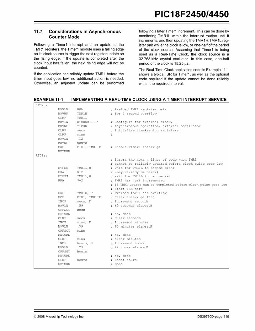
PIC18F2450/4450
© 2008 Microchip Technology Inc. DS39760D-page 119
11.7 Considerations in Asynchronous Counter Mode
Following a Timer1 interrupt and an update to theTMR1 registers, the Timer1 module uses a falling edgeon its clock source to trigger the next register update onthe rising edge. If the update is completed after theclock input has fallen, the next rising edge will not becounted.
If the application can reliably update TMR1 before thetimer input goes low, no additional action is needed.Otherwise, an adjusted update can be performed
following a later Timer1 increment. This can be done bymonitoring TMR1L within the interrupt routine until itincrements, and then updating the TMR1H:TMR1L reg-ister pair while the clock is low, or one-half of the periodof the clock source. Assuming that Timer1 is beingused as a Real-Time Clock, the clock source is a32.768 kHz crystal oscillator. In this case, one-halfperiod of the clock is 15.25 μs.
The Real-Time Clock application code in Example 11-1shows a typical ISR for Timer1, as well as the optionalcode required if the update cannot be done reliablywithin the required interval.
EXAMPLE 11-1: IMPLEMENTING A REAL-TIME CLOCK USING A TIMER1 INTERRUPT SERVICERTCinit
MOVLW 80h ; Preload TMR1 register pairMOVWF TMR1H ; for 1 second overflowCLRF TMR1LMOVLW b�00001111� ; Configure for external clock,MOVWF T1CON ; Asynchronous operation, external oscillatorCLRF secs ; Initialize timekeeping registersCLRF mins ;MOVLW .12MOVWF hoursBSF PIE1, TMR1IE ; Enable Timer1 interruptRETURN
RTCisr; Insert the next 4 lines of code when TMR1; cannot be reliably updated before clock pulse goes low
BTFSC TMR1L,0 ; wait for TMR1L to become clearBRA $-2 ; (may already be clear)BTFSS TMR1L,0 ; wait for TMR1L to become setBRA $-2 ; TMR1 has just incremented
; If TMR1 update can be completed before clock pulse goes low; Start ISR here
BSF TMR1H, 7 ; Preload for 1 sec overflowBCF PIR1, TMR1IF ; Clear interrupt flagINCF secs, F ; Increment secondsMOVLW .59 ; 60 seconds elapsed?CPFSGT secsRETURN ; No, doneCLRF secs ; Clear secondsINCF mins, F ; Increment minutesMOVLW .59 ; 60 minutes elapsed?CPFSGT minsRETURN ; No, doneCLRF mins ; clear minutesINCF hours, F ; Increment hoursMOVLW .23 ; 24 hours elapsed?CPFSGT hoursRETURN ; No, doneCLRF hours ; Reset hoursRETURN ; Done

PIC18F2450/4450
DS39760D-page 120 © 2008 Microchip Technology Inc.
TABLE 11-2: REGISTERS ASSOCIATED WITH TIMER1 AS A TIMER/COUNTER
Name Bit 7 Bit 6 Bit 5 Bit 4 Bit 3 Bit 2 Bit 1 Bit 0Reset Values
on Page:
INTCON GIE/GIEH PEIE/GIEL TMR0IE INT0IE RBIE TMR0IF INT0IF RBIF 49PIR1 � ADIF RCIF TXIF � CCP1IF TMR2IF TMR1IF 51PIE1 � ADIE RCIE TXIE � CCP1IE TMR2IE TMR1IE 51IPR1 � ADIP RCIP TXIP � CCP1IP TMR2IP TMR1IP 51TMR1L Timer1 Register Low Byte 50TMR1H TImer1 Register High Byte 50
T1CON RD16 T1RUN T1CKPS1 T1CKPS0 T1OSCEN T1SYNC TMR1CS TMR1ON 50Legend: � = unimplemented, read as �0�. Shaded cells are not used by the Timer1 module.
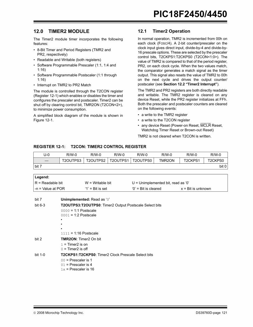
PIC18F2450/4450
© 2008 Microchip Technology Inc. DS39760D-page 121
12.0 TIMER2 MODULEThe Timer2 module timer incorporates the followingfeatures:
� 8-Bit Timer and Period Registers (TMR2 and PR2, respectively)
� Readable and Writable (both registers) � Software Programmable Prescaler (1:1, 1:4 and
1:16)� Software Programmable Postscaler (1:1 through
1:16)� Interrupt on TMR2 to PR2 Match
The module is controlled through the T2CON register(Register 12-1) which enables or disables the timer andconfigures the prescaler and postscaler. Timer2 can beshut off by clearing control bit, TMR2ON (T2CON<2>),to minimize power consumption.
A simplified block diagram of the module is shown inFigure 12-1.
12.1 Timer2 OperationIn normal operation, TMR2 is incremented from 00h oneach clock (FOSC/4). A 2-bit counter/prescaler on theclock input gives direct input, divide-by-4 and divide-by-16 prescale options. These are selected by the prescalercontrol bits, T2CKPS1:T2CKPS0 (T2CON<1:0>). Thevalue of TMR2 is compared to that of the period register,PR2, on each clock cycle. When the two values match,the comparator generates a match signal as the timeroutput. This signal also resets the value of TMR2 to 00hon the next cycle and drives the output counter/postscaler (see Section 12.2 �Timer2 Interrupt�).
The TMR2 and PR2 registers are both directly readableand writable. The TMR2 register is cleared on anydevice Reset, while the PR2 register initializes at FFh.Both the prescaler and postscaler counters are clearedon the following events:
� a write to the TMR2 register� a write to the T2CON register� any device Reset (Power-on Reset, MCLR Reset,
Watchdog Timer Reset or Brown-out Reset)
TMR2 is not cleared when T2CON is written.
REGISTER 12-1: T2CON: TIMER2 CONTROL REGISTER
U-0 R/W-0 R/W-0 R/W-0 R/W-0 R/W-0 R/W-0 R/W-0� T2OUTPS3 T2OUTPS2 T2OUTPS1 T2OUTPS0 TMR2ON T2CKPS1 T2CKPS0
bit 7 bit 0
Legend:R = Readable bit W = Writable bit U = Unimplemented bit, read as �0�-n = Value at POR �1� = Bit is set �0� = Bit is cleared x = Bit is unknown
bit 7 Unimplemented: Read as �0�bit 6-3 T2OUTPS3:T2OUTPS0: Timer2 Output Postscale Select bits
0000 = 1:1 Postscale 0001 = 1:2 Postscale � � � 1111 = 1:16 Postscale
bit 2 TMR2ON: Timer2 On bit1 = Timer2 is on 0 = Timer2 is off
bit 1-0 T2CKPS1:T2CKPS0: Timer2 Clock Prescale Select bits00 = Prescaler is 1 01 = Prescaler is 4 1x = Prescaler is 16
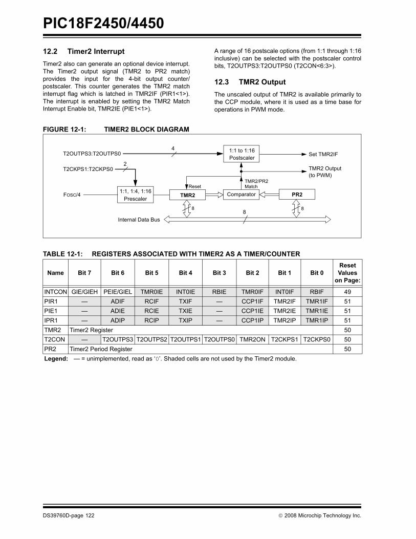
PIC18F2450/4450
DS39760D-page 122 © 2008 Microchip Technology Inc.
12.2 Timer2 InterruptTimer2 also can generate an optional device interrupt.The Timer2 output signal (TMR2 to PR2 match)provides the input for the 4-bit output counter/postscaler. This counter generates the TMR2 matchinterrupt flag which is latched in TMR2IF (PIR1<1>).The interrupt is enabled by setting the TMR2 MatchInterrupt Enable bit, TMR2IE (PIE1<1>).
A range of 16 postscale options (from 1:1 through 1:16inclusive) can be selected with the postscaler controlbits, T2OUTPS3:T2OUTPS0 (T2CON<6:3>).
12.3 TMR2 OutputThe unscaled output of TMR2 is available primarily tothe CCP module, where it is used as a time base foroperations in PWM mode.
FIGURE 12-1: TIMER2 BLOCK DIAGRAM
TABLE 12-1: REGISTERS ASSOCIATED WITH TIMER2 AS A TIMER/COUNTER
Name Bit 7 Bit 6 Bit 5 Bit 4 Bit 3 Bit 2 Bit 1 Bit 0Reset Values
on Page:
INTCON GIE/GIEH PEIE/GIEL TMR0IE INT0IE RBIE TMR0IF INT0IF RBIF 49PIR1 � ADIF RCIF TXIF � CCP1IF TMR2IF TMR1IF 51PIE1 � ADIE RCIE TXIE � CCP1IE TMR2IE TMR1IE 51IPR1 � ADIP RCIP TXIP � CCP1IP TMR2IP TMR1IP 51TMR2 Timer2 Register 50T2CON � T2OUTPS3 T2OUTPS2 T2OUTPS1 T2OUTPS0 TMR2ON T2CKPS1 T2CKPS0 50PR2 Timer2 Period Register 50Legend: � = unimplemented, read as �0�. Shaded cells are not used by the Timer2 module.
Comparator
TMR2 Output
TMR2
Postscaler
PrescalerPR2
2
FOSC/4
1:1 to 1:16
1:1, 1:4, 1:16
4T2OUTPS3:T2OUTPS0
T2CKPS1:T2CKPS0
Set TMR2IF
Internal Data Bus8
ResetTMR2/PR2
88
(to PWM)
Match

PIC18F2450/4450
© 2008 Microchip Technology Inc. DS39760D-page 123
13.0 CAPTURE/COMPARE/PWM (CCP) MODULE
PIC18F2450/4450 devices have one CCP (Capture/Compare/PWM) module. The module contains a 16-bitregister, which can operate as a 16-bit Capture register,a 16-bit Compare register or a PWM Master/Slave DutyCycle register.
REGISTER 13-1: CCP1CON: CAPTURE/COMPARE/PWM CONTROL REGISTER
U-0 U-0 R/W-0 R/W-0 R/W-0 R/W-0 R/W-0 R/W-0� � DC1B1 DC1B0 CCP1M3 CCP1M2 CCP1M1 CCP1M0
bit 7 bit 0
Legend:R = Readable bit W = Writable bit U = Unimplemented bit, read as �0�-n = Value at POR �1� = Bit is set �0� = Bit is cleared x = Bit is unknown
bit 7-6 Unimplemented: Read as �0�bit 5-4 DC1B1:DC1B0: PWM Duty Cycle for CCP Module bits
Capture mode:Unused.Compare mode:Unused.PWM mode:These bits are the two LSbs (bit 1 and bit 0) of the 10-bit PWM duty cycle. The eight MSbs of the dutycycle are found in CCPR1L.
bit 3-0 CCP1M3:CCP1M0: CCP Module Mode Select bits0000 = Capture/Compare/PWM disabled (resets CCP module) 0001 = Reserved 0010 = Compare mode: toggle output on match (CCP1IF bit is set) 0011 = Reserved 0100 = Capture mode: every falling edge 0101 = Capture mode: every rising edge0110 = Capture mode: every 4th rising edge 0111 = Capture mode: every 16th rising edge1000 = Compare mode: initialize CCP1 pin low; on compare match, force CCP1 pin high
(CCP1IF bit is set) 1001 = Compare mode: initialize CCP1 pin high; on compare match, force CCP1 pin low
(CCP1IF bit is set) 1010 = Compare mode: generate software interrupt on compare match (CCP1IF bit is set,
CCP1 pin reflects I/O state) 1011 = Compare mode: trigger special event, reset timer and start A/D conversion on CCP1 match
(CCP1IF bit is set)11xx = PWM mode

PIC18F2450/4450
DS39760D-page 124 © 2008 Microchip Technology Inc.
13.1 CCP Module ConfigurationThe Capture/Compare/PWM module is associated witha control register (generically, CCP1CON) and a dataregister (CCPR1). The data register, in turn, iscomprised of two 8-bit registers: CCPR1L (low byte)and CCPR1H (high byte). All registers are bothreadable and writable.
13.1.1 CCP MODULE AND TIMER RESOURCES
The CCP module utilizes Timer1 or Timer2, dependingon the mode selected. Timer1 is available to the mod-ule in Capture or Compare modes, while Timer2 isavailable for modules in PWM mode.
TABLE 13-1: CCP MODE � TIMER RESOURCE
In Timer1 in Asynchronous Counter mode, the captureoperation will not work.
13.2 Capture ModeIn Capture mode, the CCPR1H:CCPR1L register paircaptures the 16-bit value of the TMR1 register when anevent occurs on the corresponding CCP1 pin. An eventis defined as one of the following:
� every falling edge� every rising edge� every 4th rising edge� every 16th rising edge
The event is selected by the mode select bits,CCP1M3:CCP1M0 (CCP1CON<3:0>). When a captureis made, the interrupt request flag bit, CCP1IF, is set; itmust be cleared in software. If another capture occursbefore the value in register CCPR1 is read, the oldcaptured value is overwritten by the new captured value.
13.2.1 CCP1 PIN CONFIGURATIONIn Capture mode, the CCP1 pin should be configuredas an input by setting the corresponding TRIS directionbit.
13.2.2 SOFTWARE INTERRUPTWhen the Capture mode is changed, a false captureinterrupt may be generated. The user should keep theCCP1IE interrupt enable bit clear to avoid falseinterrupts. The interrupt flag bit, CCP1IF, should alsobe cleared following any such change in operatingmode.
13.2.3 CCP PRESCALERThere are four prescaler settings in Capture mode.They are specified as part of the operating modeselected by the mode select bits (CCP1M3:CCP1M0).Whenever the CCP module is turned off or Capturemode is disabled, the prescaler counter is cleared. Thismeans that any Reset will clear the prescaler counter.
Switching from one capture prescaler to another maygenerate an interrupt. Also, the prescaler counter willnot be cleared, therefore, the first capture may be froma non-zero prescaler. Example 13-1 shows therecommended method for switching between captureprescalers. This example also clears the prescalercounter and will not generate the �false� interrupt.
EXAMPLE 13-1: CHANGING BETWEEN CAPTURE PRESCALERS(CCP1 SHOWN)
FIGURE 13-1: CAPTURE MODE OPERATION BLOCK DIAGRAM
CCP Mode Timer Resource
CaptureCompare
PWM
Timer1 Timer1 Timer2
Note: If RC2/CCP1 is configured as an output, awrite to the port can cause a capturecondition.
CLRF CCP1CON ; Turn CCP module offMOVLW NEW_CAPT_PS ; Load WREG with the
; new prescaler mode; value and CCP ON
MOVWF CCP1CON ; Load CCP1CON with; this value
CCPR1H CCPR1L
TMR1H TMR1L
Set CCP1IF
Q1:Q4CCP1CON<3:0>
CCP1 pinPrescaler÷ 1, 4, 16
andEdge Detect
TMR1Enable
44
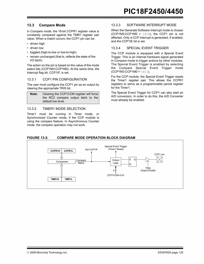
PIC18F2450/4450
© 2008 Microchip Technology Inc. DS39760D-page 125
13.3 Compare ModeIn Compare mode, the 16-bit CCPR1 register value isconstantly compared against the TMR1 register pairvalue. When a match occurs, the CCP1 pin can be:
� driven high� driven low� toggled (high-to-low or low-to-high) � remain unchanged (that is, reflects the state of the
I/O latch)
The action on the pin is based on the value of the modeselect bits (CCP1M3:CCP1M0). At the same time, theinterrupt flag bit, CCP1IF, is set.
13.3.1 CCP1 PIN CONFIGURATIONThe user must configure the CCP1 pin as an output byclearing the appropriate TRIS bit.
13.3.2 TIMER1 MODE SELECTIONTimer1 must be running in Timer mode, orSynchronized Counter mode, if the CCP module isusing the compare feature. In Asynchronous Countermode, the compare operation may not work.
13.3.3 SOFTWARE INTERRUPT MODE When the Generate Software Interrupt mode is chosen(CCP1M3:CCP1M0 = 1010), the CCP1 pin is notaffected. Only a CCP interrupt is generated, if enabled,and the CCP1IE bit is set.
13.3.4 SPECIAL EVENT TRIGGERThe CCP module is equipped with a Special EventTrigger. This is an internal hardware signal generatedin Compare mode to trigger actions by other modules.The Special Event Trigger is enabled by selectingthe Compare Special Event Trigger mode(CCP1M3:CCP1M0 = 1011).
For the CCP module, the Special Event Trigger resetsthe Timer1 register pair. This allows the CCPR1registers to serve as a programmable period registerfor the Timer1.
The Special Event Trigger for CCP1 can also start anA/D conversion. In order to do this, the A/D Convertermust already be enabled.
FIGURE 13-2: COMPARE MODE OPERATION BLOCK DIAGRAM
Note: Clearing the CCP1CON register will forcethe RC2 compare output latch to thedefault low level.
CCPR1H CCPR1L
TMR1H TMR1L
ComparatorQS
R
OutputLogic
Special Event TriggerSet CCP1IF
CCP1 pin
TRIS
CCP1CON<3:0>
Output Enable
Compare
4
(Timer1 Reset)
Match

PIC18F2450/4450
DS39760D-page 126 © 2008 Microchip Technology Inc.
TABLE 13-2: REGISTERS ASSOCIATED WITH CAPTURE, COMPARE, TIMER1
Name Bit 7 Bit 6 Bit 5 Bit 4 Bit 3 Bit 2 Bit 1 Bit 0Reset Values
on Page:
INTCON GIE/GIEH PEIE/GIEL TMR0IE INT0IE RBIE TMR0IF INT0IF RBIF 49
RCON IPEN SBOREN(1) � RI TO PD POR BOR 50PIR1 � ADIF RCIF TXIF � CCP1IF TMR2IF TMR1IF 51PIE1 � ADIE RCIE TXIE � CCP1IE TMR2IE TMR1IE 51IPR1 � ADIP RCIP TXIP � CCP1IP TMR2IP TMR1IP 51TRISC TRISC7 TRISC6 � � � TRISC2 TRISC1 TRISC0 51TMR1L Timer1 Register Low Byte 50TMR1H Timer1 Register High Byte 50
T1CON RD16 T1RUN T1CKPS1 T1CKPS0 T1OSCEN T1SYNC TMR1CS TMR1ON 50CCPR1L Capture/Compare/PWM Register 1 Low Byte 50CCPR1H Capture/Compare/PWM Register 1 High Byte 50CCP1CON � � DC1B1 DC1B0 CCP1M3 CCP1M2 CCP1M1 CCP1M0 50Legend: � = unimplemented, read as �0�. Shaded cells are not used by capture/compare and Timer1.Note 1: The SBOREN bit is only available when BOREN<1:0> = 01; otherwise, the bit reads as �0�.

PIC18F2450/4450
© 2008 Microchip Technology Inc. DS39760D-page 127
13.4 PWM ModeIn Pulse-Width Modulation (PWM) mode, the CCP1 pinproduces up to a 10-bit resolution PWM output.
Figure 13-3 shows a simplified block diagram of theCCP module in PWM mode.
For a step-by-step procedure on how to set up the CCPmodule for PWM operation, see Section 13.4.3�Setup for PWM Operation�.
FIGURE 13-3: SIMPLIFIED PWM BLOCK DIAGRAM
A PWM output (Figure 13-4) has a time base (period)and a time that the output stays high (duty cycle).The frequency of the PWM is the inverse of theperiod (1/period).
FIGURE 13-4: PWM OUTPUT
13.4.1 PWM PERIODThe PWM period is specified by writing to the PR2register. The PWM period can be calculated using thefollowing formula:
EQUATION 13-1:
PWM frequency is defined as 1/[PWM period].
When TMR2 is equal to PR2, the following three eventsoccur on the next increment cycle:
� TMR2 is cleared� The CCP1 pin is set (exception: if PWM duty
cycle = 0%, the CCP1 pin will not be set)� The PWM duty cycle is latched from CCPR1L into
CCPR1H
13.4.2 PWM DUTY CYCLEThe PWM duty cycle is specified by writing to theCCPR1L register and to the CCP1CON<5:4> bits. Upto 10-bit resolution is available. The CCPR1L containsthe eight MSbs and the CCP1CON<5:4> bits containthe two LSbs. This 10-bit value is represented byCCPR1L:CCP1CON<5:4>. Equation 13-2 is used tocalculate the PWM duty cycle in time:
EQUATION 13-2:
CCPR1L and CCP1CON<5:4> can be written to at anytime, but the duty cycle value is not latched intoCCPR1H until after a match between PR2 and TMR2occurs (i.e., the period is complete). In PWM mode,CCPR1H is a read-only register.
CCPR1L
CCPR1H (Slave)
Comparator
TMR2
Comparator
PR2
(Note 1)
R Q
S
Duty Cycle Registers CCP1CON<5:4>
Clear Timer,CCP1 pin and latch D.C.
Note 1: The 8-bit TMR2 value is concatenated with the 2-bit internal Q clock, or 2 bits of the prescaler, to create the 10-bit time base.
CCP1
CorrespondingTRIS bit
Output
Period
Duty Cycle
TMR2 = PR2
TMR2 = Duty Cycle
TMR2 = PR2
Note: The Timer2 postscalers (see Section 12.0�Timer2 Module�) are not used in thedetermination of the PWM frequency. Thepostscaler could be used to have a servoupdate rate at a different frequency thanthe PWM output.
PWM Period = [(PR2) + 1] � 4 � TOSC �(TMR2 Prescale Value)
PWM Duty Cycle = (CCPR1L:CCP1CON<5:4>) �TOSC � (TMR2 Prescale Value)
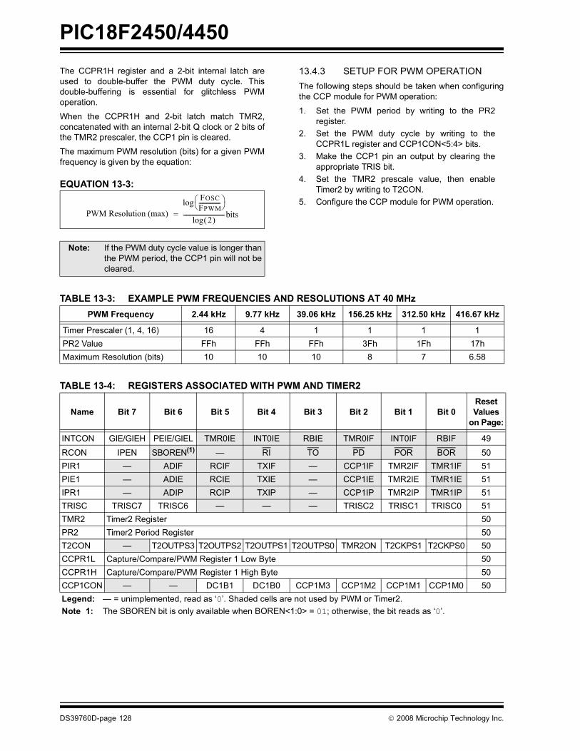
PIC18F2450/4450
DS39760D-page 128 © 2008 Microchip Technology Inc.
The CCPR1H register and a 2-bit internal latch areused to double-buffer the PWM duty cycle. Thisdouble-buffering is essential for glitchless PWMoperation.
When the CCPR1H and 2-bit latch match TMR2,concatenated with an internal 2-bit Q clock or 2 bits ofthe TMR2 prescaler, the CCP1 pin is cleared.
The maximum PWM resolution (bits) for a given PWMfrequency is given by the equation:
EQUATION 13-3:
13.4.3 SETUP FOR PWM OPERATIONThe following steps should be taken when configuringthe CCP module for PWM operation:
1. Set the PWM period by writing to the PR2register.
2. Set the PWM duty cycle by writing to theCCPR1L register and CCP1CON<5:4> bits.
3. Make the CCP1 pin an output by clearing theappropriate TRIS bit.
4. Set the TMR2 prescale value, then enableTimer2 by writing to T2CON.
5. Configure the CCP module for PWM operation.
TABLE 13-3: EXAMPLE PWM FREQUENCIES AND RESOLUTIONS AT 40 MHz
TABLE 13-4: REGISTERS ASSOCIATED WITH PWM AND TIMER2
Note: If the PWM duty cycle value is longer thanthe PWM period, the CCP1 pin will not becleared.
FOSCFPWM---------------⎝ ⎠
⎛ ⎞log
2( )log-----------------------------bits=PWM Resolution (max)
PWM Frequency 2.44 kHz 9.77 kHz 39.06 kHz 156.25 kHz 312.50 kHz 416.67 kHz
Timer Prescaler (1, 4, 16) 16 4 1 1 1 1PR2 Value FFh FFh FFh 3Fh 1Fh 17hMaximum Resolution (bits) 10 10 10 8 7 6.58
Name Bit 7 Bit 6 Bit 5 Bit 4 Bit 3 Bit 2 Bit 1 Bit 0Reset Values
on Page:
INTCON GIE/GIEH PEIE/GIEL TMR0IE INT0IE RBIE TMR0IF INT0IF RBIF 49
RCON IPEN SBOREN(1) � RI TO PD POR BOR 50PIR1 � ADIF RCIF TXIF � CCP1IF TMR2IF TMR1IF 51PIE1 � ADIE RCIE TXIE � CCP1IE TMR2IE TMR1IE 51IPR1 � ADIP RCIP TXIP � CCP1IP TMR2IP TMR1IP 51TRISC TRISC7 TRISC6 � � � TRISC2 TRISC1 TRISC0 51TMR2 Timer2 Register 50PR2 Timer2 Period Register 50T2CON � T2OUTPS3 T2OUTPS2 T2OUTPS1 T2OUTPS0 TMR2ON T2CKPS1 T2CKPS0 50CCPR1L Capture/Compare/PWM Register 1 Low Byte 50CCPR1H Capture/Compare/PWM Register 1 High Byte 50CCP1CON � � DC1B1 DC1B0 CCP1M3 CCP1M2 CCP1M1 CCP1M0 50Legend: � = unimplemented, read as �0�. Shaded cells are not used by PWM or Timer2.Note 1: The SBOREN bit is only available when BOREN<1:0> = 01; otherwise, the bit reads as �0�.

PIC18F2450/4450
© 2008 Microchip Technology Inc. DS39760D-page 129
14.0 UNIVERSAL SERIAL BUS (USB)
This section describes the details of the USB peripheral.Because of the very specific nature of the module,knowledge of USB is expected. Some high-level USBinformation is provided in Section 14.9 �Overview ofUSB� only for application design reference. Designersare encouraged to refer to the official specificationpublished by the USB Implementers Forum (USB-IF) forthe latest information. USB Specification Revision 2.0 isthe most current specification at the time of publicationof this document.
14.1 Overview of the USB PeripheralThe PIC18F2450/4450 device family contains a full-speed and low-speed, compatible USB Serial InterfaceEngine (SIE) that allows fast communication between
any USB host and the PIC® microcontroller. The SIE canbe interfaced directly to the USB, utilizing the internaltransceiver, or it can be connected through an externaltransceiver. An internal 3.3V regulator is also availableto power the internal transceiver in 5V applications.
Some special hardware features have been included toimprove performance. Dual port memory in thedevice�s data memory space (USB RAM) has beensupplied to share direct memory access between themicrocontroller core and the SIE. Buffer descriptors arealso provided, allowing users to freely programendpoint memory usage within the USB RAM space.
Figure 14-1 presents a general overview of the USBperipheral and its features.
FIGURE 14-1: USB PERIPHERAL AND OPTIONS
UOE(1)
256-ByteUSB RAM
USBSIE
USB Control and VM(1)
VP(1)
RCV(1)
VMO(1)
VPO(1)
ExternalTransceiver
EN
3.3V Regulator
D+D-
VUSBExternal 3.3V
Supply(3)
USB Clock from theOscillator Module
Configuration
VREGEN
ExternalPull-ups(2)
(Low(Full
PIC18F2450/4450 Family
USB Bus
USB Bus
Speed) Speed)
Note 1: This signal is only available if the internal transceiver is disabled (UTRDIS = 1).2: The pull-ups can be supplied either from the VUSB pin or from an external 3.3V supply.3: Do not enable the internal regulator when using an external 3.3V supply.
Transceiver
P
PInternal Pull-ups
OE
FSENUPUEN
UTRDIS
FS
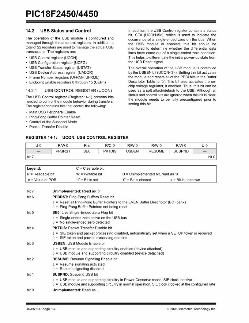
PIC18F2450/4450
DS39760D-page 130 © 2008 Microchip Technology Inc.
14.2 USB Status and ControlThe operation of the USB module is configured andmanaged through three control registers. In addition, atotal of 22 registers are used to manage the actual USBtransactions. The registers are:
� USB Control register (UCON)� USB Configuration register (UCFG)� USB Transfer Status register (USTAT)� USB Device Address register (UADDR)� Frame Number registers (UFRMH:UFRML)� Endpoint Enable registers 0 through 15 (UEPn)
14.2.1 USB CONTROL REGISTER (UCON)The USB Control register (Register 14-1) contains bitsneeded to control the module behavior during transfers.The register contains bits that control the following:
� Main USB Peripheral Enable� Ping-Pong Buffer Pointer Reset� Control of the Suspend Mode� Packet Transfer Disable
In addition, the USB Control register contains a statusbit, SE0 (UCON<5>), which is used to indicate theoccurrence of a single-ended zero on the bus. Whenthe USB module is enabled, this bit should bemonitored to determine whether the differential datalines have come out of a single-ended zero condition.This helps to differentiate the initial power-up state fromthe USB Reset signal.
The overall operation of the USB module is controlledby the USBEN bit (UCON<3>). Setting this bit activatesthe module and resets all of the PPBI bits in the BufferDescriptor Table to �0�. This bit also activates the on-chip voltage regulator, if enabled. Thus, this bit can beused as a soft attach/detach to the USB. Although allstatus and control bits are ignored when this bit is clear,the module needs to be fully preconfigured prior tosetting this bit.
REGISTER 14-1: UCON: USB CONTROL REGISTER
U-0 R/W-0 R-x R/C-0 R/W-0 R/W-0 R/W-0 U-0� PPBRST SE0 PKTDIS USBEN RESUME SUSPND �
bit 7 bit 0
Legend: C = Clearable bitR = Readable bit W = Writable bit U = Unimplemented bit, read as �0�-n = Value at POR �1� = Bit is set �0� = Bit is cleared x = Bit is unknown
bit 7 Unimplemented: Read as �0�bit 6 PPBRST: Ping-Pong Buffers Reset bit
1 = Reset all Ping-Pong Buffer Pointers to the EVEN Buffer Descriptor (BD) banks0 = Ping-Pong Buffer Pointers not being reset
bit 5 SE0: Live Single-Ended Zero Flag bit1 = Single-ended zero active on the USB bus0 = No single-ended zero detected
bit 4 PKTDIS: Packet Transfer Disable bit1 = SIE token and packet processing disabled, automatically set when a SETUP token is received0 = SIE token and packet processing enabled
bit 3 USBEN: USB Module Enable bit1 = USB module and supporting circuitry enabled (device attached)0 = USB module and supporting circuitry disabled (device detached)
bit 2 RESUME: Resume Signaling Enable bit1 = Resume signaling activated0 = Resume signaling disabled
bit 1 SUSPND: Suspend USB bit1 = USB module and supporting circuitry in Power Conserve mode, SIE clock inactive0 = USB module and supporting circuitry in normal operation, SIE clock clocked at the configured rate
bit 0 Unimplemented: Read as �0�

PIC18F2450/4450
© 2008 Microchip Technology Inc. DS39760D-page 131
The PPBRST bit (UCON<6>) controls the Reset statuswhen Double-Buffering mode (ping-pong buffering) isused. When the PPBRST bit is set, all Ping-PongBuffer Pointers are set to the EVEN buffers. PPBRSThas to be cleared by firmware. This bit is ignored inbuffering modes not using ping-pong buffering.
The PKTDIS bit (UCON<4>) is a flag indicating that theSIE has disabled packet transmission and reception.This bit is set by the SIE when a SETUP token isreceived to allow setup processing. This bit cannot beset by the microcontroller, only cleared; clearing itallows the SIE to continue transmission and/orreception. Any pending events within the BufferDescriptor Table will still be available, indicated withinthe USTAT register�s FIFO buffer.
The RESUME bit (UCON<2>) allows the peripheral toperform a remote wake-up by executing Resumesignaling. To generate a valid remote wake-up,firmware must set RESUME for 10 ms and then clearthe bit. For more information on Resume signaling, seeSections 7.1.7.5, 11.4.4 and 11.9 in the USB 2.0Specification.
The SUSPND bit (UCON<1>) places the module andsupporting circuitry (i.e., voltage regulator) in a low-power mode. The input clock to the SIE is alsodisabled. This bit should be set by the software inresponse to an IDLEIF interrupt. It should be reset bythe microcontroller firmware after an ACTVIF interruptis observed. When this bit is active, the device remainsattached to the bus but the transceiver outputs remainIdle. The voltage on the VUSB pin may vary dependingon the value of this bit. Setting this bit before a IDLEIFrequest will result in unpredictable bus behavior.
14.2.2 USB CONFIGURATION REGISTER (UCFG)
Prior to communicating over USB, the module�sassociated internal and/or external hardware must beconfigured. Most of the configuration is performed withthe UCFG register (Register 14-2). The separate USBvoltage regulator (see Section 14.2.2.8 �InternalRegulator�) is controlled through the Configurationregisters.
The UFCG register contains most of the bits thatcontrol the system level behavior of the USB module.These include:
� Bus Speed (full speed versus low speed)� On-Chip Transceiver Enable� Ping-Pong Buffer Usage
The UCFG register also contains two bits which aid inmodule testing, debugging and USB certifications.These bits control output enable state monitoring andeye pattern generation.
14.2.2.1 Internal TransceiverThe USB peripheral has a built-in, USB 2.0, full-speedand low-speed compliant transceiver, internally con-nected to the SIE. This feature is useful for low-cost,single chip applications. The UTRDIS bit (UCFG<3>)controls the transceiver; it is enabled by default(UTRDIS = 0). The FSEN bit (UCFG<2>) controls thetransceiver speed; setting the bit enables full-speedoperation. The on-chip USB pull-up resistors are con-trolled by the UPUEN bit (UCFG<4>). They can only beselected when the on-chip transceiver is enabled.
The USB specification requires 3.3V operation forcommunications; however, the rest of the chip may berunning at a higher voltage. Thus, the transceiver issupplied power from a separate source, VUSB.
14.2.2.2 External TransceiverThis module provides support for use with an off-chiptransceiver. The off-chip transceiver is intended forapplications where physical conditions dictate thelocation of the transceiver to be away from the SIE. Forexample, applications that require isolation from theUSB could use an external transceiver through someisolation to the microcontroller�s SIE (Figure 14-2).External transceiver operation is enabled by setting theUTRDIS bit.
FIGURE 14-2: TYPICAL EXTERNAL TRANSCEIVER WITH ISOLATION
Note: While in Suspend mode, a typical buspowered USB device is limited to 500 μAof current. This is the complete currentdrawn by the PIC microcontroller and itssupporting circuitry. Care should be takento assure minimum current draw when thedevice enters Suspend mode.
Note: The USB speed, transceiver and pull-upshould only be configured during the mod-ule setup phase. It is not recommended toswitch these settings while the module isenabled.
PIC®
Microcontroller
Transceiver
VPOUOE
Note: The above setting shows a simplified schematicfor a full-speed configuration using an externaltransceiver with isolation.
VPRCVVMO
VM
D+D-
Isolation1.5 kΩ
3.3V Derivedfrom USB
VUSBVDD
VDD Isolatedfrom USB

PIC18F2450/4450
DS39760D-page 132 © 2008 Microchip Technology Inc.
There are 6 signals from the module to communicatewith and control an external transceiver:
� VM: Input from the single-ended D- line � VP: Input from the single-ended D+ line� RCV: Input from the differential receiver� VMO: Output to the differential line driver� VPO: Output to the differential line driver� UOE: Output enable
The VPO and VMO signals are outputs from the SIE tothe external transceiver. The RCV signal is the outputfrom the external transceiver to the SIE; it representsthe differential signals from the serial bus translatedinto a single pulse train. The VM and VP signals areused to report conditions on the serial bus to the SIEthat can�t be captured with the RCV signal. Thecombinations of states of these signals and theirinterpretation are listed in Table 14-1 and Table 14-2.
REGISTER 14-2: UCFG: USB CONFIGURATION REGISTER
R/W-0 R/W-0 U-0 R/W-0 R/W-0 R/W-0 R/W-0 R/W-0UTEYE UOEMON(1) � UPUEN(2,3) UTRDIS(2) FSEN(2) PPB1 PPB0
bit 7 bit 0
Legend:R = Readable bit W = Writable bit U = Unimplemented bit, read as �0�-n = Value at POR �1� = Bit is set �0� = Bit is cleared x = Bit is unknown
bit 7 UTEYE: USB Eye Pattern Test Enable bit1 = Eye pattern test enabled0 = Eye pattern test disabled
bit 6 UOEMON: USB OE Monitor Enable bit(1)
1 = UOE signal active; it indicates intervals during which the D+/D- lines are driving0 = UOE signal inactive
bit 5 Unimplemented: Read as �0�bit 4 UPUEN: USB On-Chip Pull-up Enable bit(2,3)
1 = On-chip pull-up enabled (pull-up on D+ with FSEN = 1 or D- with FSEN = 0)0 = On-chip pull-up disabled
bit 3 UTRDIS: On-Chip Transceiver Disable bit(2)
1 = On-chip transceiver disabled; digital transceiver interface enabled0 = On-chip transceiver active
bit 2 FSEN: Full-Speed Enable bit(2)
1 = Full-speed device: controls transceiver edge rates; requires input clock at 48 MHz0 = Low-speed device: controls transceiver edge rates; requires input clock at 6 MHz
bit 1-0 PPB1:PPB0: Ping-Pong Buffers Configuration bits11 = Enabled for all endpoints except Endpoint 010 = EVEN/ODD ping-pong buffers enabled for all endpoints01 = EVEN/ODD ping-pong buffer enabled for OUT Endpoint 000 = EVEN/ODD ping-pong buffers disabled
Note 1: If UTRDIS is set, the UOE signal will be active independent of the UOEMON bit setting.2: The UPUEN, UTRDIS and FSEN bits should never be changed while the USB module is enabled. These
values must be preconfigured prior to enabling the module.3: This bit is only valid when the on-chip transceiver is active (UTRDIS = 0); otherwise, it is ignored.
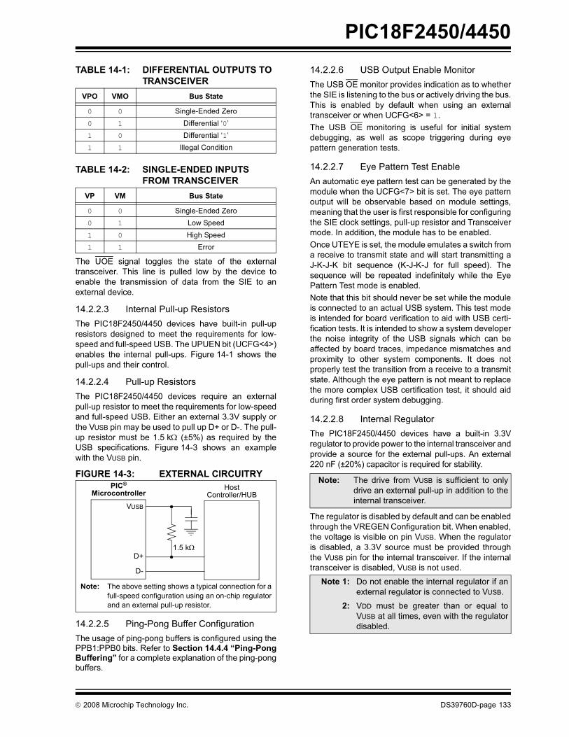
PIC18F2450/4450
© 2008 Microchip Technology Inc. DS39760D-page 133
TABLE 14-1: DIFFERENTIAL OUTPUTS TO TRANSCEIVER
TABLE 14-2: SINGLE-ENDED INPUTS FROM TRANSCEIVER
The UOE signal toggles the state of the externaltransceiver. This line is pulled low by the device toenable the transmission of data from the SIE to anexternal device.
14.2.2.3 Internal Pull-up ResistorsThe PIC18F2450/4450 devices have built-in pull-upresistors designed to meet the requirements for low-speed and full-speed USB. The UPUEN bit (UCFG<4>)enables the internal pull-ups. Figure 14-1 shows thepull-ups and their control.
14.2.2.4 Pull-up ResistorsThe PIC18F2450/4450 devices require an externalpull-up resistor to meet the requirements for low-speedand full-speed USB. Either an external 3.3V supply orthe VUSB pin may be used to pull up D+ or D-. The pull-up resistor must be 1.5 kΩ (±5%) as required by theUSB specifications. Figure 14-3 shows an examplewith the VUSB pin.
FIGURE 14-3: EXTERNAL CIRCUITRY
14.2.2.5 Ping-Pong Buffer ConfigurationThe usage of ping-pong buffers is configured using thePPB1:PPB0 bits. Refer to Section 14.4.4 �Ping-PongBuffering� for a complete explanation of the ping-pongbuffers.
14.2.2.6 USB Output Enable Monitor The USB OE monitor provides indication as to whetherthe SIE is listening to the bus or actively driving the bus.This is enabled by default when using an externaltransceiver or when UCFG<6> = 1.The USB OE monitoring is useful for initial systemdebugging, as well as scope triggering during eyepattern generation tests.
14.2.2.7 Eye Pattern Test EnableAn automatic eye pattern test can be generated by themodule when the UCFG<7> bit is set. The eye patternoutput will be observable based on module settings,meaning that the user is first responsible for configuringthe SIE clock settings, pull-up resistor and Transceivermode. In addition, the module has to be enabled.Once UTEYE is set, the module emulates a switch froma receive to transmit state and will start transmitting aJ-K-J-K bit sequence (K-J-K-J for full speed). Thesequence will be repeated indefinitely while the EyePattern Test mode is enabled.Note that this bit should never be set while the moduleis connected to an actual USB system. This test modeis intended for board verification to aid with USB certi-fication tests. It is intended to show a system developerthe noise integrity of the USB signals which can beaffected by board traces, impedance mismatches andproximity to other system components. It does notproperly test the transition from a receive to a transmitstate. Although the eye pattern is not meant to replacethe more complex USB certification test, it should aidduring first order system debugging.
14.2.2.8 Internal RegulatorThe PIC18F2450/4450 devices have a built-in 3.3Vregulator to provide power to the internal transceiver andprovide a source for the external pull-ups. An external220 nF (±20%) capacitor is required for stability.
The regulator is disabled by default and can be enabledthrough the VREGEN Configuration bit. When enabled,the voltage is visible on pin VUSB. When the regulatoris disabled, a 3.3V source must be provided throughthe VUSB pin for the internal transceiver. If the internaltransceiver is disabled, VUSB is not used.
VPO VMO Bus State
0 0 Single-Ended Zero0 1 Differential �0�1 0 Differential �1�1 1 Illegal Condition
VP VM Bus State
0 0 Single-Ended Zero0 1 Low Speed1 0 High Speed1 1 Error
PIC®
MicrocontrollerHost
Controller/HUBVUSB
D+
D-
Note: The above setting shows a typical connection for afull-speed configuration using an on-chip regulatorand an external pull-up resistor.
1.5 kΩ
Note: The drive from VUSB is sufficient to onlydrive an external pull-up in addition to theinternal transceiver.
Note 1: Do not enable the internal regulator if anexternal regulator is connected to VUSB.
2: VDD must be greater than or equal toVUSB at all times, even with the regulatordisabled.
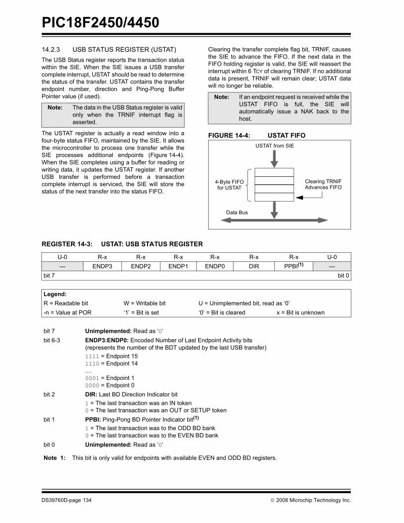
PIC18F2450/4450
DS39760D-page 134 © 2008 Microchip Technology Inc.
14.2.3 USB STATUS REGISTER (USTAT)The USB Status register reports the transaction statuswithin the SIE. When the SIE issues a USB transfercomplete interrupt, USTAT should be read to determinethe status of the transfer. USTAT contains the transferendpoint number, direction and Ping-Pong BufferPointer value (if used).
The USTAT register is actually a read window into afour-byte status FIFO, maintained by the SIE. It allowsthe microcontroller to process one transfer while theSIE processes additional endpoints (Figure 14-4).When the SIE completes using a buffer for reading orwriting data, it updates the USTAT register. If anotherUSB transfer is performed before a transactioncomplete interrupt is serviced, the SIE will store thestatus of the next transfer into the status FIFO.
Clearing the transfer complete flag bit, TRNIF, causesthe SIE to advance the FIFO. If the next data in theFIFO holding register is valid, the SIE will reassert theinterrupt within 6 TCY of clearing TRNIF. If no additionaldata is present, TRNIF will remain clear; USTAT datawill no longer be reliable.
FIGURE 14-4: USTAT FIFO
Note: The data in the USB Status register is validonly when the TRNIF interrupt flag isasserted.
Note: If an endpoint request is received while theUSTAT FIFO is full, the SIE willautomatically issue a NAK back to thehost.
Data Bus
USTAT from SIE
4-Byte FIFOfor USTAT
Clearing TRNIFAdvances FIFO
REGISTER 14-3: USTAT: USB STATUS REGISTER
U-0 R-x R-x R-x R-x R-x R-x U-0� ENDP3 ENDP2 ENDP1 ENDP0 DIR PPBI(1) �
bit 7 bit 0
Legend:R = Readable bit W = Writable bit U = Unimplemented bit, read as �0�-n = Value at POR �1� = Bit is set �0� = Bit is cleared x = Bit is unknown
bit 7 Unimplemented: Read as �0�bit 6-3 ENDP3:ENDP0: Encoded Number of Last Endpoint Activity bits
(represents the number of the BDT updated by the last USB transfer)1111 = Endpoint 151110 = Endpoint 14....0001 = Endpoint 10000 = Endpoint 0
bit 2 DIR: Last BD Direction Indicator bit1 = The last transaction was an IN token0 = The last transaction was an OUT or SETUP token
bit 1 PPBI: Ping-Pong BD Pointer Indicator bit(1)
1 = The last transaction was to the ODD BD bank0 = The last transaction was to the EVEN BD bank
bit 0 Unimplemented: Read as �0�
Note 1: This bit is only valid for endpoints with available EVEN and ODD BD registers.
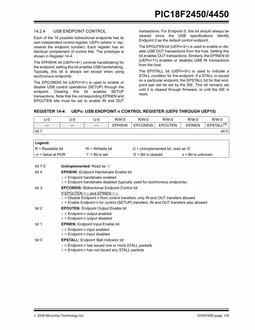
PIC18F2450/4450
© 2008 Microchip Technology Inc. DS39760D-page 135
14.2.4 USB ENDPOINT CONTROLEach of the 16 possible bidirectional endpoints has itsown independent control register, UEPn (where �n� rep-resents the endpoint number). Each register has anidentical complement of control bits. The prototype isshown in Register 14-4.
The EPHSHK bit (UEPn<4>) controls handshaking forthe endpoint; setting this bit enables USB handshaking.Typically, this bit is always set except when usingisochronous endpoints.
The EPCONDIS bit (UEPn<3>) is used to enable ordisable USB control operations (SETUP) through theendpoint. Clearing this bit enables SETUPtransactions. Note that the corresponding EPINEN andEPOUTEN bits must be set to enable IN and OUT
transactions. For Endpoint 0, this bit should always becleared since the USB specifications identifyEndpoint 0 as the default control endpoint.
The EPOUTEN bit (UEPn<2>) is used to enable or dis-able USB OUT transactions from the host. Setting thisbit enables OUT transactions. Similarly, the EPINEN bit(UEPn<1>) enables or disables USB IN transactionsfrom the host.
The EPSTALL bit (UEPn<0>) is used to indicate aSTALL condition for the endpoint. If a STALL is issuedon a particular endpoint, the EPSTALL bit for that end-point pair will be set by the SIE. This bit remains setuntil it is cleared through firmware, or until the SIE isreset.
REGISTER 14-4: UEPn: USB ENDPOINT n CONTROL REGISTER (UEP0 THROUGH UEP15)
U-0 U-0 U-0 R/W-0 R/W-0 R/W-0 R/W-0 R/W-0� � � EPHSHK EPCONDIS EPOUTEN EPINEN EPSTALL(1)
bit 7 bit 0
Legend:R = Readable bit W = Writable bit U = Unimplemented bit, read as �0�-n = Value at POR �1� = Bit is set �0� = Bit is cleared x = Bit is unknown
bit 7-5 Unimplemented: Read as �0�bit 4 EPHSHK: Endpoint Handshake Enable bit
1 = Endpoint handshake enabled0 = Endpoint handshake disabled (typically used for isochronous endpoints)
bit 3 EPCONDIS: Bidirectional Endpoint Control bitIf EPOUTEN = 1 and EPINEN = 1:1 = Disable Endpoint n from control transfers; only IN and OUT transfers allowed0 = Enable Endpoint n for control (SETUP) transfers; IN and OUT transfers also allowed
bit 2 EPOUTEN: Endpoint Output Enable bit1 = Endpoint n output enabled0 = Endpoint n output disabled
bit 1 EPINEN: Endpoint Input Enable bit1 = Endpoint n input enabled0 = Endpoint n input disabled
bit 0 EPSTALL: Endpoint Stall Indicator bit1 = Endpoint n has issued one or more STALL packets0 = Endpoint n has not issued any STALL packets

PIC18F2450/4450
DS39760D-page 136 © 2008 Microchip Technology Inc.
14.2.5 USB ADDRESS REGISTER (UADDR)
The USB Address register contains the unique USBaddress that the peripheral will decode when active.UADDR is reset to 00h when a USB Reset is received,indicated by URSTIF, or when a Reset is received fromthe microcontroller. The USB address must be writtenby the microcontroller during the USB setup phase(enumeration) as part of the Microchip USB firmwaresupport.
14.2.6 USB FRAME NUMBER REGISTERS (UFRMH:UFRML)
The Frame Number registers contain the 11-bit framenumber. The low-order byte is contained in UFRML,while the three high-order bits are contained inUFRMH. The register pair is updated with the currentframe number whenever a SOF token is received. Forthe microcontroller, these registers are read-only. TheFrame Number register is primarily used forisochronous transfers.
14.3 USB RAMUSB data moves between the microcontroller core andthe SIE through a memory space known as the USBRAM. This is a special dual port memory that ismapped into the normal data memory space in Bank 4(400h to 4FFh) for a total of 256 bytes (Figure 14-5).
Some portion of Bank 4 (400h through 4FFh) is usedspecifically for endpoint buffer control, while theremaining portion is available for USB data. Dependingon the type of buffering being used, all but 8 bytes ofBank 4 may also be available for use as USB bufferspace.
Although USB RAM is available to the microcontrolleras data memory, the sections that are being accessedby the SIE should not be accessed by themicrocontroller. A semaphore mechanism is used todetermine the access to a particular buffer at any giventime. This is discussed in Section 14.4.1.1 �BufferOwnership�.
FIGURE 14-5: IMPLEMENTATION OF USB RAM IN DATA MEMORY SPACE
400h
4FFh
7FFh
500h
USB Data or
Buffer Descriptors,USB Data or User Data
User Data
User Data
Unused
SFRs
3FFh
000h
F80hFFFh
Banks 0
Banks 5
Bank15
F00h
800h
to 14
to 1
Bank 4
Banks 2to 3 UnusedUnused
1FFh200h

PIC18F2450/4450
© 2008 Microchip Technology Inc. DS39760D-page 137
14.4 Buffer Descriptors and the Buffer Descriptor Table
The registers in Bank 4 are used specifically for end-point buffer control in a structure known as the BufferDescriptor Table (BDT). This provides a flexible methodfor users to construct and control endpoint buffers ofvarious lengths and configuration.
The BDT is composed of Buffer Descriptors (BD) whichare used to define and control the actual buffers in theUSB RAM space. Each BD, in turn, consists of fourregisters, where n represents one of the 64 possibleBDs (range of 0 to 63):
� BDnSTAT: BD Status register� BDnCNT: BD Byte Count register� BDnADRL: BD Address Low register� BDnADRH: BD Address High register
BDs always occur as a four-byte block in the sequence,BDnSTAT:BDnCNT:BDnADRL:BDnADRH. The addressof BDnSTAT is always an offset of (4n � 1) (inhexadecimal) from 400h, with n being the bufferdescriptor number.
Depending on the buffering configuration used(Section 14.4.4 �Ping-Pong Buffering�), there are upto 32, 33 or 64 sets of buffer descriptors. At a minimum,the BDT must be at least 8 bytes long. This is becausethe USB specification mandates that every device musthave Endpoint 0 with both input and output for initialsetup. Depending on the endpoint and bufferingconfiguration, the BDT can be as long as 256 bytes.
Although they can be thought of as Special FunctionRegisters, the Buffer Descriptor Status and Addressregisters are not hardware mapped, as conventionalmicrocontroller SFRs in Bank 15 are. If the endpoint cor-responding to a particular BD is not enabled, its registersare not used. Instead of appearing as unimplementedaddresses, however, they appear as available RAM.Only when an endpoint is enabled by setting theUEPn<1> bit does the memory at those addressesbecome functional as BD registers. As with any addressin the data memory space, the BD registers have anindeterminate value on any device Reset.
A total of 256 bytes of address space in Bank 4 isavailable for BDT and USB data RAM. In Ping-PongBuffer mode, all the 16 bidirectional endpoints can notbe implemented where BDT itself can be as long as256 bytes. In the majority of USB applications, fewendpoints are required to be implemented. Hence, asmall portion of the 256 bytes will be used for BDT andthe rest can be used for USB data.
An example of a BD for a 16-byte buffer, starting at480h, is shown in Figure 14-6. A particular set of BDregisters is only valid if the corresponding endpoint hasbeen enabled using the UEPn register. All BD registersare available in USB RAM. The BD for each endpointshould be set up prior to enabling the endpoint.
14.4.1 BD STATUS AND CONFIGURATIONBuffer descriptors not only define the size of anendpoint buffer, but also determine its configurationand control. Most of the configuration is done with theBD Status register, BDnSTAT. Each BD has its ownunique and correspondingly numbered BDnSTATregister.
FIGURE 14-6: EXAMPLE OF A BUFFER DESCRIPTOR
Unlike other control registers, the bit configuration forthe BDnSTAT register is context sensitive. There aretwo distinct configurations, depending on whether themicrocontroller or the USB module is modifying the BDand buffer at a particular time. Only three bit definitionsare shared between the two.
14.4.1.1 Buffer OwnershipBecause the buffers and their BDs are shared betweenthe CPU and the USB module, a simple semaphoremechanism is used to distinguish which is allowed toupdate the BD and associated buffers in memory.
This is done by using the UOWN bit (BDnSTAT<7>) asa semaphore to distinguish which is allowed to updatethe BD and associated buffers in memory. UOWN is theonly bit that is shared between the two configurationsof BDnSTAT.
When UOWN is clear, the BD entry is �owned� by themicrocontroller core. When the UOWN bit is set, the BDentry and the buffer memory are �owned� by the USBperipheral. The core should not modify the BD or itscorresponding data buffer during this time. Note thatthe microcontroller core can still read BDnSTAT whilethe SIE owns the buffer and vice versa.
The buffer descriptors have a different meaning basedon the source of the register update. Prior to placingownership with the USB peripheral, the user can con-figure the basic operation of the peripheral through theBDnSTAT bits. During this time, the byte count andbuffer location registers can also be set.
400h
USB Data
Buffer
Buffer
BD0STATBD0CNT
BD0ADRLBD0ADRH
401h402h403h
480h
48Fh
Descriptor
Note: Memory regions are not to scale.
10h80h04h
Starting
Size of Block
(xxh)
RegistersAddress Contents
Address
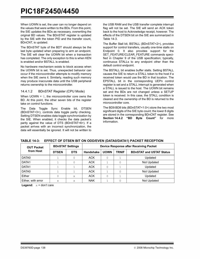
PIC18F2450/4450
DS39760D-page 138 © 2008 Microchip Technology Inc.
When UOWN is set, the user can no longer depend onthe values that were written to the BDs. From this point,the SIE updates the BDs as necessary, overwriting theoriginal BD values. The BDnSTAT register is updatedby the SIE with the token PID and the transfer count,BDnCNT, is updated.
The BDnSTAT byte of the BDT should always be thelast byte updated when preparing to arm an endpoint.The SIE will clear the UOWN bit when a transactionhas completed. The only exception to this is when KENis enabled and/or BSTALL is enabled.
No hardware mechanism exists to block access whenthe UOWN bit is set. Thus, unexpected behavior canoccur if the microcontroller attempts to modify memorywhen the SIE owns it. Similarly, reading such memorymay produce inaccurate data until the USB peripheralreturns ownership to the microcontroller.
14.4.1.2 BDnSTAT Register (CPU Mode)When UOWN = 0, the microcontroller core owns theBD. At this point, the other seven bits of the registertake on control functions.
The Data Toggle Sync Enable bit, DTSEN(BDnSTAT<3>), controls data toggle parity checking.Setting DTSEN enables data toggle synchronization bythe SIE. When enabled, it checks the data packet�sparity against the value of DTS (BDnSTAT<6>). If apacket arrives with an incorrect synchronization, thedata will essentially be ignored. It will not be written to
the USB RAM and the USB transfer complete interruptflag will not be set. The SIE will send an ACK tokenback to the host to Acknowledge receipt, however. Theeffects of the DTSEN bit on the SIE are summarized inTable 14-3.
The Buffer Stall bit, BSTALL (BDnSTAT<2>), providessupport for control transfers, usually one-time stalls onEndpoint 0. It also provides support for theSET_FEATURE/CLEAR_FEATURE commands speci-fied in Chapter 9 of the USB specification; typically,continuous STALLs to any endpoint other than thedefault control endpoint.
The BSTALL bit enables buffer stalls. Setting BSTALLcauses the SIE to return a STALL token to the host if areceived token would use the BD in that location. TheEPSTALL bit in the corresponding UEPn controlregister is set and a STALL interrupt is generated whena STALL is issued to the host. The UOWN bit remainsset and the BDs are not changed unless a SETUPtoken is received. In this case, the STALL condition iscleared and the ownership of the BD is returned to themicrocontroller core.
The BD9:BD8 bits (BDnSTAT<1:0>) store the two mostsignificant digits of the SIE byte count; the lower 8 digitsare stored in the corresponding BDnCNT register. SeeSection 14.4.2 �BD Byte Count� for moreinformation.
TABLE 14-3: EFFECT OF DTSEN BIT ON ODD/EVEN (DATA0/DATA1) PACKET RECEPTION
OUT Packetfrom Host
BDnSTAT Settings Device Response after Receiving Packet
DTSEN DTS Handshake UOWN TRNIF BDnSTAT and USTAT Status
DATA0 1 0 ACK 0 1 UpdatedDATA1 1 0 ACK 1 0 Not UpdatedDATA1 1 1 ACK 0 1 UpdatedDATA0 1 1 ACK 1 0 Not UpdatedEither 0 x ACK 0 1 UpdatedEither, with error x x NAK 1 0 Not UpdatedLegend: x = don�t care

PIC18F2450/4450
© 2008 Microchip Technology Inc. DS39760D-page 139
REGISTER 14-5: BDnSTAT: BUFFER DESCRIPTOR n STATUS REGISTER (BD0STAT THROUGH
BD63STAT), CPU MODE (DATA IS WRITTEN TO THE SIDE)
R/W-x R/W-x R/W-x R/W-x R/W-x R/W-x R/W-x R/W-xUOWN(1) DTS(2) �(3) �(3) DTSEN BSTALL BC9 BC8
bit 7 bit 0
Legend:R = Readable bit W = Writable bit U = Unimplemented bit, read as �0�-n = Value at POR �1� = Bit is set �0� = Bit is cleared x = Bit is unknown
bit 7 UOWN: USB Own bit(1)
0 = The microcontroller core owns the BD and its corresponding bufferbit 6 DTS: Data Toggle Synchronization bit(2)
1 = Data 1 packet0 = Data 0 packet
bit 5-4 Reserved: These bits should always be programmed to �0�(3)
bit 3 DTSEN: Data Toggle Synchronization Enable bit1 = Data toggle synchronization is enabled; data packets with incorrect Sync value will be ignored
except for a SETUP transaction, which is accepted even if the data toggle bits do not match.0 = No data toggle synchronization is performed
bit 2 BSTALL: Buffer Stall Enable bit1 = Buffer stall enabled; STALL handshake issued if a token is received that would use the BD in the
given location (UOWN bit remains set, BD value is unchanged)0 = Buffer stall disabled
bit 1-0 BC9:BC8: Byte Count 9 and 8 bitsThe byte count bits represent the number of bytes that will be transmitted for an IN token or receivedduring an OUT token. Together with BC<7:0>, the valid byte counts are 0-1023.
Note 1: This bit must be initialized by the user to the desired value prior to enabling the USB module.2: This bit is ignored unless DTSEN = 1.3: If these bits are set, USB communication may not work. Hence, these bits should always be maintained
as �0�.
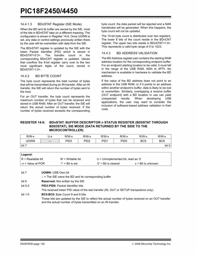
PIC18F2450/4450
DS39760D-page 140 © 2008 Microchip Technology Inc.
14.4.1.3 BDnSTAT Register (SIE Mode)When the BD and its buffer are owned by the SIE, mostof the bits in BDnSTAT take on a different meaning. Theconfiguration is shown in Register 14-6. Once UOWN isset, any data or control settings previously written thereby the user will be overwritten with data from the SIE.
The BDnSTAT register is updated by the SIE with thetoken Packet Identifier (PID) which is stored inBDnSTAT<5:3>. The transfer count in thecorresponding BDnCNT register is updated. Valuesthat overflow the 8-bit register carry over to the twomost significant digits of the count, stored inBDnSTAT<1:0>.
14.4.2 BD BYTE COUNTThe byte count represents the total number of bytesthat will be transmitted during an IN transfer. After an INtransfer, the SIE will return the number of bytes sent tothe host.
For an OUT transfer, the byte count represents themaximum number of bytes that can be received andstored in USB RAM. After an OUT transfer, the SIE willreturn the actual number of bytes received. If thenumber of bytes received exceeds the corresponding
byte count, the data packet will be rejected and a NAKhandshake will be generated. When this happens, thebyte count will not be updated.
The 10-bit byte count is distributed over two registers.The lower 8 bits of the count reside in the BDnCNTregister. The upper two bits reside in BDnSTAT<1:0>.This represents a valid byte range of 0 to 1023.
14.4.3 BD ADDRESS VALIDATIONThe BD Address register pair contains the starting RAMaddress location for the corresponding endpoint buffer.For an endpoint starting location to be valid, it must fallin the range of the USB RAM, 400h to 4FFh. Nomechanism is available in hardware to validate the BDaddress.
If the value of the BD address does not point to anaddress in the USB RAM, or if it points to an addresswithin another endpoint�s buffer, data is likely to be lostor overwritten. Similarly, overlapping a receive buffer(OUT endpoint) with a BD location in use can yieldunexpected results. When developing USBapplications, the user may want to consider theinclusion of software-based address validation in theircode.
REGISTER 14-6: BDnSTAT: BUFFER DESCRIPTOR n STATUS REGISTER (BD0STAT THROUGH
BD63STAT), SIE MODE (DATA RETURNED BY THE SIDE TO THE MICROCONTROLLER)
R/W-x U-x R/W-x R/W-x R/W-x R/W-x R/W-x R/W-xUOWN � PID3 PID2 PID1 PID0 BC9 BC8
bit 7 bit 0
Legend:R = Readable bit W = Writable bit U = Unimplemented bit, read as �0�-n = Value at POR �1� = Bit is set �0� = Bit is cleared x = Bit is unknown
bit 7 UOWN: USB Own bit1 = The SIE owns the BD and its corresponding buffer
bit 6 Reserved: Not written by the SIEbit 5-2 PID3:PID0: Packet Identifier bits
The received token PID value of the last transfer (IN, OUT or SETUP transactions only).bit 1-0 BC9:BC8: Byte Count 9 and 8 bits
These bits are updated by the SIE to reflect the actual number of bytes received on an OUT transferand the actual number of bytes transmitted on an IN transfer.

PIC18F2450/4450
© 2008 Microchip Technology Inc. DS39760D-page 141
14.4.4 PING-PONG BUFFERINGAn endpoint is defined to have a ping-pong buffer whenit has two sets of BD entries: one set for an EVENtransfer and one set for an ODD transfer. This allowsthe CPU to process one BD while the SIE is processingthe other BD. Double-buffering BDs in this way allowsfor maximum throughput to/from the USB.
The USB module supports three modes of operation:
� No ping-pong support� Ping-pong buffer support for OUT Endpoint 0 only� Ping-pong buffer support for all endpoints
The ping-pong buffer settings are configured using thePPB1:PPB0 bits in the UCFG register.
The USB module keeps track of the Ping-Pong Pointerindividually for each endpoint. All pointers are initiallyreset to the EVEN BD when the module is enabled.After the completion of a transaction (UOWN cleared
by the SIE), the pointer is toggled to the ODD BD. Afterthe completion of the next transaction, the pointer istoggled back to the EVEN BD and so on.
The EVEN/ODD status of the last transaction is storedin the PPBI bit of the USTAT register. The user canreset all Ping-Pong Pointers to EVEN using thePPBRST bit.
Figure 14-7 shows the three different modes ofoperation and how USB RAM is filled with the BDs.
BDs have a fixed relationship to a particular endpoint,depending on the buffering configuration. The mappingof BDs to endpoints is detailed in Table 14-4. Thisrelationship also means that gaps may occur in theBDT if endpoints are not enabled contiguously. Thistheoretically means that the BDs for disabled endpointscould be used as buffer space. In practice, usersshould avoid using such spaces in the BDT unless amethod of validating BD addresses is implemented.
FIGURE 14-7: BUFFER DESCRIPTOR TABLE MAPPING FOR BUFFERING MODES
EP1 IN EVEN
EP1 OUT EVEN
EP1 OUT ODD
EP1 IN ODD
Descriptor
Descriptor
Descriptor
Descriptor
EP1 IN
EP15 IN
EP1 OUT
EP0 OUT
PPB1:PPB0 = 00
EP0 IN
EP1 IN
No Ping-Pong Buffers
EP15 IN
EP0 IN
EP0 OUT EVEN
PPB1:PPB0 = 01
EP0 OUT ODD
EP1 OUT
Ping-Pong Buffer on EP0 OUT
EP15 IN ODD
EP0 IN EVEN
EP0 OUT EVEN
PPB1:PPB0 = 10
EP0 OUT ODD
EP0 IN ODD
Ping-Pong Buffers on All EPs
Descriptor
Descriptor
Descriptor
Descriptor
Descriptor
Descriptor
Descriptor
Descriptor
Descriptor
Descriptor
Descriptor
Descriptor
400h
4FFh 4FFh 4FFh
400h 400h
47Fh
483h
Availableas
Data RAM Availableas
Data RAM
Maximum Memory Used: 128 bytesMaximum BDs: 32 (BD0 to BD31)
Maximum Memory Used: 132 bytesMaximum BDs: 33 (BD0 to BD32)
Maximum Memory Used: 256 bytesMaximum BDs: 64 (BD0 to BD63)
Note: Memory area not shown to scale.
Descriptor
Descriptor
Descriptor
Descriptor
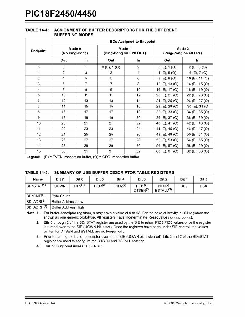
PIC18F2450/4450
DS39760D-page 142 © 2008 Microchip Technology Inc.
TABLE 14-4: ASSIGNMENT OF BUFFER DESCRIPTORS FOR THE DIFFERENT BUFFERING MODES
TABLE 14-5: SUMMARY OF USB BUFFER DESCRIPTOR TABLE REGISTERS
Endpoint
BDs Assigned to Endpoint
Mode 0(No Ping-Pong)
Mode 1(Ping-Pong on EP0 OUT)
Mode 2(Ping-Pong on all EPs)
Out In Out In Out In
0 0 1 0 (E), 1 (O) 2 0 (E), 1 (O) 2 (E), 3 (O)1 2 3 3 4 4 (E), 5 (O) 6 (E), 7 (O)2 4 5 5 6 8 (E), 9 (O) 10 (E), 11 (O)3 6 7 7 8 12 (E), 13 (O) 14 (E), 15 (O)4 8 9 9 10 16 (E), 17 (O) 18 (E), 19 (O)5 10 11 11 12 20 (E), 21 (O) 22 (E), 23 (O)6 12 13 13 14 24 (E), 25 (O) 26 (E), 27 (O)7 14 15 15 16 28 (E), 29 (O) 30 (E), 31 (O)8 16 17 17 18 32 (E), 33 (O) 34 (E), 35 (O)9 18 19 19 20 36 (E), 37 (O) 38 (E), 39 (O)
10 20 21 21 22 40 (E), 41 (O) 42 (E), 43 (O)11 22 23 23 24 44 (E), 45 (O) 46 (E), 47 (O)12 24 25 25 26 48 (E), 49 (O) 50 (E), 51 (O)13 26 27 27 28 52 (E), 53 (O) 54 (E), 55 (O)14 28 29 29 30 56 (E), 57 (O) 58 (E), 59 (O)15 30 31 31 32 60 (E), 61 (O) 62 (E), 63 (O)
Legend: (E) = EVEN transaction buffer, (O) = ODD transaction buffer
Name Bit 7 Bit 6 Bit 5 Bit 4 Bit 3 Bit 2 Bit 1 Bit 0
BDnSTAT(1) UOWN DTS(4) PID3(2) PID2(2) PID1(2)
DTSEN(3)PID0(2)
BSTALL(3)BC9 BC8
BDnCNT(1) Byte CountBDnADRL(1) Buffer Address LowBDnADRH(1) Buffer Address HighNote 1: For buffer descriptor registers, n may have a value of 0 to 63. For the sake of brevity, all 64 registers are
shown as one generic prototype. All registers have indeterminate Reset values (xxxx xxxx).2: Bits 5 through 2 of the BDnSTAT register are used by the SIE to return PID3:PID0 values once the register
is turned over to the SIE (UOWN bit is set). Once the registers have been under SIE control, the values written for DTSEN and BSTALL are no longer valid.
3: Prior to turning the buffer descriptor over to the SIE (UOWN bit is cleared), bits 3 and 2 of the BDnSTAT register are used to configure the DTSEN and BSTALL settings.
4: This bit is ignored unless DTSEN = 1.

PIC18F2450/4450
© 2008 Microchip Technology Inc. DS39760D-page 143
14.5 USB InterruptsThe USB module can generate multiple interruptconditions. To accommodate all of these interruptsources, the module is provided with its own interruptlogic structure, similar to that of the microcontroller.USB interrupts are enabled with one set of control regis-ters and trapped with a separate set of flag registers. Allsources are funneled into a single USB interruptrequest, USBIF (PIR2<5>), in the microcontroller�sinterrupt logic.
Figure 14-8 shows the interrupt logic for the USBmodule. There are two layers of interrupt registers inthe USB module. The top level consists of overall USBstatus interrupts; these are enabled and flagged in theUIE and UIR registers, respectively. The second levelconsists of USB error conditions, which are enabledand flagged in the UEIR and UEIE registers. Aninterrupt condition in any of these triggers a USB ErrorInterrupt Flag (UERRIF) in the top level.
Interrupts may be used to trap routine events in a USBtransaction. Figure 14-9 shows some common eventswithin a USB frame and their corresponding interrupts.
FIGURE 14-8: USB INTERRUPT LOGIC FUNNEL
FIGURE 14-9: EXAMPLE OF A USB TRANSACTION AND INTERRUPT EVENTS
BTSEFBTSEEBTOEFBTOEE
DFN8EFDFN8EE
CRC16EFCRC16EE
CRC5EFCRC5EE
PIDEFPIDEE
SOFIFSOFIE
TRNIFTRNIE
IDLEIFIDLEIE
STALLIFSTALLIE
ACTVIFACTVIE
URSTIFURSTIE
UERRIFUERRIE
USBIF
Second Level USB Interrupts(USB Error Conditions)
UEIR (Flag) and UEIE (Enable) Registers
Top Level USB Interrupts(USB Status Interrupts)
UIR (Flag) and UIE (Enable) Registers
USB Reset
SOFRESET SETUP DATA STATUS SOF
SETUPToken Data ACK
OUT Token Empty Data ACKStart-of-Frame (SOF)
IN Token Data ACK
SOFIF
URSTIF
1 ms Frame
Differential Data
From Host From Host To Host
From Host To Host From Host
From Host From Host To Host
Transaction
Control Transfer(1)
TransactionComplete
Note 1: The control transfer shown here is only an example showing events that can occur for every transaction. Typical control transfers will spread across multiple frames.
Set TRNIF
Set TRNIF
Set TRNIF

PIC18F2450/4450
DS39760D-page 144 © 2008 Microchip Technology Inc.
14.5.1 USB INTERRUPT STATUS REGISTER (UIR)
The USB Interrupt Status register (Register 14-7)contains the flag bits for each of the USB statusinterrupt sources. Each of these sources has acorresponding interrupt enable bit in the UIE register. Allof the USB status flags are ORed together to generatethe USBIF interrupt flag for the microcontroller�sinterrupt funnel.
Once an interrupt bit has been set by the SIE, it mustbe cleared by software by writing a �0�. The flag bitscan also be set in software which can aid in firmwaredebugging.
When the USB module is in the Low-Power Suspendmode (UCON<1> = 1), the SIE does not get clocked.When in this state, the SIE cannot process packets,and therefore, cannot detect new interrupt conditionsother than the Activity Detect Interrupt, Flag ACTVIF.The ACTVIF bit is typically used by USB firmware todetect when the microcontroller should bring the USBmodule out of the Low-Power Suspend mode(UCON<1> = 0).
REGISTER 14-7: UIR: USB INTERRUPT STATUS REGISTER
U-0 R/W-0 R/W-0 R/W-0 R/W-0 R/W-0 R-0 R/W-0� SOFIF STALLIF IDLEIF(1) TRNIF(2) ACTVIF(3) UERRIF(4) URSTIF
bit 7 bit 0
Legend:R = Readable bit W = Writable bit U = Unimplemented bit, read as �0�-n = Value at POR �1� = Bit is set �0� = Bit is cleared x = Bit is unknown
bit 7 Unimplemented: Read as �0�bit 6 SOFIF: Start-of-Frame Token Interrupt bit
1 = A Start-of-Frame token received by the SIE0 = No Start-of-Frame token received by the SIE
bit 5 STALLIF: A STALL Handshake Interrupt bit1 = A STALL handshake was sent by the SIE0 = A STALL handshake has not been sent
bit 4 IDLEIF: Idle Detect Interrupt bit(1)
1 = Idle condition detected (constant Idle state of 3 ms or more)0 = No Idle condition detected
bit 3 TRNIF: Transaction Complete Interrupt bit(2)
1 = Processing of pending transaction is complete; read USTAT register for endpoint information0 = Processing of pending transaction is not complete or no transaction is pending
bit 2 ACTVIF: Bus Activity Detect Interrupt bit(3)
1 = Activity on the D+/D- lines was detected0 = No activity detected on the D+/D- lines
bit 1 UERRIF: USB Error Condition Interrupt bit(4)
1 = An unmasked error condition has occurred0 = No unmasked error condition has occurred.
bit 0 URSTIF: USB Reset Interrupt bit1 = Valid USB Reset occurred; 00h is loaded into UADDR register0 = No USB Reset has occurred
Note 1: Once an Idle state is detected, the user may want to place the USB module in Suspend mode.2: Clearing this bit will cause the USTAT FIFO to advance (valid only for IN, OUT and SETUP tokens).3: This bit is typically unmasked only following the detection of a UIDLE interrupt event.4: Only error conditions enabled through the UEIE register will set this bit. This bit is a status bit only and
cannot be set or cleared by the user.

PIC18F2450/4450
© 2008 Microchip Technology Inc. DS39760D-page 145
14.5.1.1 Bus Activity Detect Interrupt Bit (ACTVIF)
The ACTVIF bit cannot be cleared immediately afterthe USB module wakes up from Suspend or while theUSB module is suspended. A few clock cycles arerequired to synchronize the internal hardware statemachine before the ACTVIF bit can be cleared byfirmware. Clearing the ACTVIF bit before the internalhardware is synchronized may not have an effect onthe value of ACTVIF. Additionally, if the USB moduleuses the clock from the 96 MHz PLL source, then afterclearing the SUSPND bit, the USB module may not beimmediately operational while waiting for the 96 MHzPLL to lock. The application code should clear theACTVIF bit as shown in Example 14-1.
Only one ACTVIF interrupt is generated when resum-ing from the USB bus Idle condition. If user firmwareclears the ACTVIF bit, the bit will not immediatelybecome set again, even when there is continuous bustraffic. Bus traffic must cease long enough to generateanother IDLEIF condition before another ACTVIFinterrupt can be generated.
EXAMPLE 14-1: CLEARING ACTVIF BIT (UIR<2>)
Assembly:BCF UCON, SUSPND
LOOP:BTFSS UIR, ACTVIFBRA DONEBCF UIR, ACTVIFBRA LOOP
DONE
C:UCONbits.SUSPND = 0;while (UIRbits.ACTVIF){UIRbits.ACTVIF = 0};

PIC18F2450/4450
DS39760D-page 146 © 2008 Microchip Technology Inc.
14.5.2 USB INTERRUPT ENABLE REGISTER (UIE)
The USB Interrupt Enable register (Register 14-8)contains the enable bits for the USB status interruptsources. Setting any of these bits will enable therespective interrupt source in the UIR register.
The values in this register only affect the propagationof an interrupt condition to the microcontroller�sinterrupt logic. The flag bits are still set by theirinterrupt conditions, allowing them to be polled andserviced without actually generating an interrupt.
REGISTER 14-8: UIE: USB INTERRUPT ENABLE REGISTER
U-0 R/W-0 R/W-0 R/W-0 R/W-0 R/W-0 R/W-0 R/W-0� SOFIE STALLIE IDLEIE TRNIE ACTVIE UERRIE URSTIE
bit 7 bit 0
Legend:R = Readable bit W = Writable bit U = Unimplemented bit, read as �0�-n = Value at POR �1� = Bit is set �0� = Bit is cleared x = Bit is unknown
bit 7 Unimplemented: Read as �0�bit 6 SOFIE: Start-of-Frame Token Interrupt Enable bit
1 = Start-of-Frame token interrupt enabled0 = Start-of-Frame token interrupt disabled
bit 5 STALLIE: STALL Handshake Interrupt Enable bit1 = STALL interrupt enabled0 = STALL interrupt disabled
bit 4 IDLEIE: Idle Detect Interrupt Enable bit1 = Idle detect interrupt enabled0 = Idle detect interrupt disabled
bit 3 TRNIE: Transaction Complete Interrupt Enable bit1 = Transaction interrupt enabled0 = Transaction interrupt disabled
bit 2 ACTVIE: Bus Activity Detect Interrupt Enable bit1 = Bus activity detect interrupt enabled0 = Bus activity detect interrupt disabled
bit 1 UERRIE: USB Error Interrupt Enable bit1 = USB error interrupt enabled0 = USB error interrupt disabled
bit 0 URSTIE: USB Reset Interrupt Enable bit1 = USB Reset interrupt enabled0 = USB Reset interrupt disabled

PIC18F2450/4450
© 2008 Microchip Technology Inc. DS39760D-page 147
14.5.3 USB ERROR INTERRUPT STATUS REGISTER (UEIR)
The USB Error Interrupt Status register (Register 14-9)contains the flag bits for each of the error sourceswithin the USB peripheral. Each of these sources iscontrolled by a corresponding interrupt enable bit inthe UEIE register. All of the USB error flags are ORedtogether to generate the USB Error Interrupt Flag(UERRIF) at the top level of the interrupt logic.
Each error bit is set as soon as the error condition isdetected. Thus, the interrupt will typically notcorrespond with the end of a token being processed.
Once an interrupt bit has been set by the SIE, it mustbe cleared by software by writing a �0�.
REGISTER 14-9: UEIR: USB ERROR INTERRUPT STATUS REGISTER
R/C-0 U-0 U-0 R/C-0 R/C-0 R/C-0 R/C-0 R/C-0BTSEF � � BTOEF DFN8EF CRC16EF CRC5EF PIDEF
bit 7 bit 0
Legend:R = Readable bit C = Clearable bit U = Unimplemented bit, read as �0�-n = Value at POR �1� = Bit is set �0� = Bit is cleared x = Bit is unknown
bit 7 BTSEF: Bit Stuff Error Flag bit1 = A bit stuff error has been detected0 = No bit stuff error
bit 6-5 Unimplemented: Read as �0�bit 4 BTOEF: Bus Turnaround Time-out Error Flag bit
1 = Bus turnaround time-out has occurred (more than 16 bit times of Idle from previous EOP elapsed)0 = No bus turnaround time-out
bit 3 DFN8EF: Data Field Size Error Flag bit1 = The data field was not an integral number of bytes0 = The data field was an integral number of bytes
bit 2 CRC16EF: CRC16 Failure Flag bit1 = The CRC16 failed0 = The CRC16 passed
bit 1 CRC5EF: CRC5 Host Error Flag bit1 = The token packet was rejected due to a CRC5 error0 = The token packet was accepted
bit 0 PIDEF: PID Check Failure Flag bit1 = PID check failed0 = PID check passed
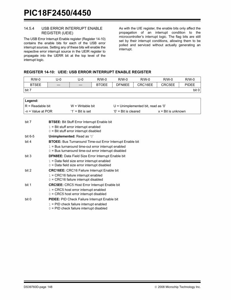
PIC18F2450/4450
DS39760D-page 148 © 2008 Microchip Technology Inc.
14.5.4 USB ERROR INTERRUPT ENABLE REGISTER (UEIE)
The USB Error Interrupt Enable register (Register 14-10)contains the enable bits for each of the USB errorinterrupt sources. Setting any of these bits will enable therespective error interrupt source in the UEIR register topropagate into the UERR bit at the top level of theinterrupt logic.
As with the UIE register, the enable bits only affect thepropagation of an interrupt condition to themicrocontroller�s interrupt logic. The flag bits are stillset by their interrupt conditions, allowing them to bepolled and serviced without actually generating aninterrupt.
REGISTER 14-10: UEIE: USB ERROR INTERRUPT ENABLE REGISTER
R/W-0 U-0 U-0 R/W-0 R/W-0 R/W-0 R/W-0 R/W-0BTSEE � � BTOEE DFN8EE CRC16EE CRC5EE PIDEE
bit 7 bit 0
Legend:R = Readable bit W = Writable bit U = Unimplemented bit, read as �0�-n = Value at POR �1� = Bit is set �0� = Bit is cleared x = Bit is unknown
bit 7 BTSEE: Bit Stuff Error Interrupt Enable bit1 = Bit stuff error interrupt enabled0 = Bit stuff error interrupt disabled
bit 6-5 Unimplemented: Read as �0�bit 4 BTOEE: Bus Turnaround Time-out Error Interrupt Enable bit
1 = Bus turnaround time-out error interrupt enabled0 = Bus turnaround time-out error interrupt disabled
bit 3 DFN8EE: Data Field Size Error Interrupt Enable bit1 = Data field size error interrupt enabled0 = Data field size error interrupt disabled
bit 2 CRC16EE: CRC16 Failure Interrupt Enable bit1 = CRC16 failure interrupt enabled0 = CRC16 failure interrupt disabled
bit 1 CRC5EE: CRC5 Host Error Interrupt Enable bit1 = CRC5 host error interrupt enabled0 = CRC5 host error interrupt disabled
bit 0 PIDEE: PID Check Failure Interrupt Enable bit1 = PID check failure interrupt enabled0 = PID check failure interrupt disabled
PIC18F2450/4450
© 2008 Microchip Technology Inc. DS39760D-page 149
14.6 USB Power ModesMany USB applications will likely have several differentsets of power requirements and configuration. Themost common power modes encountered are BusPower Only, Self-Power Only and Dual Power withSelf-Power Dominance. The most common cases arepresented here.
14.6.1 BUS POWER ONLYIn Bus Power Only mode, all power for the applicationis drawn from the USB (Figure 14-10). This iseffectively the simplest power method for the device.
In order to meet the inrush current requirements of theUSB 2.0 specifications, the total effective capacitanceappearing across VBUS and ground must be no morethan 10 μF; otherwise, some kind of inrush limiting isrequired. For more details, see Section 7.2.4 of theUSB 2.0 specification.
According to the USB 2.0 specification, all USB devicesmust also support a Low-Power Suspend mode. In theUSB Suspend mode, devices must consume no morethan 500 A (or 2.5 mA for high-powered devices thatare capable of remote wake-up) from the 5V VBUS lineof the USB cable.
The host signals the USB device to enter the Suspendmode by stopping all USB traffic to that device for morethan 3 ms. This condition will set the IDLEIF bit in theUIR register.
During the USB Suspend mode, the D+ or D- pull-upresistor must remain active, which will consume someof the allowed suspend current: 500A/2.5 mA budget.
FIGURE 14-10: BUS POWER ONLY
14.6.2 SELF-POWER ONLYIn Self-Power Only mode, the USB application providesits own power, with very little power being pulled fromthe USB. Figure 14-11 shows an example. Note that anattach indication is added to show when the USB hasbeen connected and the host is actively poweringVBUS.
In order to meet compliance specifications, the USBmodule (and the D+ or D- pull-up resistor) should notbe enabled until the host actively drives VBUS high. Oneof the I/O pins may be used for this purpose.The application should never source any current ontothe 5V VBUS pin of the USB cable.
FIGURE 14-11: SELF-POWER ONLY
14.6.3 DUAL POWER WITH SELF-POWER DOMINANCE
Some applications may require a dual power option.This allows the application to use internal power prima-rily, but switch to power from the USB when no internalpower is available. Figure 14-12 shows a simple DualPower with Self-Power Dominance example, whichautomatically switches between Self-Power Only andUSB Bus Power Only modes.
FIGURE 14-12: DUAL POWER EXAMPLE
Dual power devices must also meet all of the specialrequirements for inrush current and Suspend modecurrent, and must not enable the USB module untilVBUS is driven high. For descriptions of those require-ments, see Section 14.6.1 �Bus Power Only� andSection 14.6.2 �Self-Power Only�. Additionally, dualpower devices must never source current onto the 5VVUSB pin of the USB cable.
VDD
VUSB
VSS
VBUS~5V
Note: Users should keep in mind the limits fordevices drawing power from the USB.According to USB Specification 2.0, thiscannot exceed 100 mA per low-powerdevice or 500 mA per high-power device.
VDD
VUSB
VSS
VSELF~5V
I/O pinAttach Sense
100 kΩ
VBUS~5V
100 kΩ
VDD
VUSB
I/O pin
VSS
Attach Sense
VBUS
VSELF
100 kΩ
~5V
~5V
100 kΩ
PIC18F2450/4450
DS39760D-page 150 © 2008 Microchip Technology Inc.
14.7 OscillatorThe USB module has specific clock requirements. Forfull-speed operation, the clock source must be 48 MHz.Even so, the microcontroller core and other peripheralsare not required to run at that clock speed or even fromthe same clock source. Available clocking options aredescribed in detail in Section 2.3 �Oscillator Settingsfor USB�.
14.8 USB Firmware and DriversMicrochip provides a number of application-specificresources, such as USB firmware and driver support.Refer to www.microchip.com for the latest firmware anddriver support.
TABLE 14-6: REGISTERS ASSOCIATED WITH USB MODULE OPERATION(1)
Name Bit 7 Bit 6 Bit 5 Bit 4 Bit 3 Bit 2 Bit 1 Bit 0 Details on Page:
INTCON GIE/GIEH PEIE/GIEL TMR0IE INT0IE RBIE TMR0IF INT0IF RBIF 49IPR2 OSCFIP � USBIP � � HLVDIP � � 51PIR2 OSCFIF � USBIF � � HLVDIF � � 51PIE2 OSCFIE � USBIE � � HLVDIE � � 51UCON � PPBRST SE0 PKTDIS USBEN RESUME SUSPND � 52UCFG UTEYE UOEMON � UPUEN UTRDIS FSEN PPB1 PPB0 52USTAT � ENDP3 ENDP2 ENDP1 ENDP0 DIR PPBI � 52UADDR � ADDR6 ADDR5 ADDR4 ADDR3 ADDR2 ADDR1 ADDR0 52UFRML FRM7 FRM6 FRM5 FRM4 FRM3 FRM2 FRM1 FRM0 52UFRMH � � � � � FRM10 FRM9 FRM8 52UIR � SOFIF STALLIF IDLEIF TRNIF ACTVIF UERRIF URSTIF 52UIE � SOFIE STALLIE IDLEIE TRNIE ACTVIE UERRIE URSTIE 52UEIR BTSEF � � BTOEF DFN8EF CRC16EF CRC5EF PIDEF 52UEIE BTSEE � � BTOEE DFN8EE CRC16EE CRC5EE PIDEE 52UEP0 � � � EPHSHK EPCONDIS EPOUTEN EPINEN EPSTALL 52UEP1 � � � EPHSHK EPCONDIS EPOUTEN EPINEN EPSTALL 52UEP2 � � � EPHSHK EPCONDIS EPOUTEN EPINEN EPSTALL 52UEP3 � � � EPHSHK EPCONDIS EPOUTEN EPINEN EPSTALL 52UEP4 � � � EPHSHK EPCONDIS EPOUTEN EPINEN EPSTALL 52UEP5 � � � EPHSHK EPCONDIS EPOUTEN EPINEN EPSTALL 52UEP6 � � � EPHSHK EPCONDIS EPOUTEN EPINEN EPSTALL 52UEP7 � � � EPHSHK EPCONDIS EPOUTEN EPINEN EPSTALL 52UEP8 � � � EPHSHK EPCONDIS EPOUTEN EPINEN EPSTALL 52UEP9 � � � EPHSHK EPCONDIS EPOUTEN EPINEN EPSTALL 52UEP10 � � � EPHSHK EPCONDIS EPOUTEN EPINEN EPSTALL 51UEP11 � � � EPHSHK EPCONDIS EPOUTEN EPINEN EPSTALL 51UEP12 � � � EPHSHK EPCONDIS EPOUTEN EPINEN EPSTALL 51UEP13 � � � EPHSHK EPCONDIS EPOUTEN EPINEN EPSTALL 51UEP14 � � � EPHSHK EPCONDIS EPOUTEN EPINEN EPSTALL 51UEP15 � � � EPHSHK EPCONDIS EPOUTEN EPINEN EPSTALL 51Legend: � = unimplemented, read as �0�. Shaded cells are not used by the USB module.Note 1: This table includes only those hardware mapped SFRs located in Bank 15 of the data memory space. The Buffer
Descriptor registers, which are mapped into Bank 4 and are not true SFRs, are listed separately in Table 14-5.

PIC18F2450/4450
© 2008 Microchip Technology Inc. DS39760D-page 151
14.9 Overview of USBThis section presents some of the basic USB conceptsand useful information necessary to design a USBdevice. Although much information is provided in thissection, there is a plethora of information providedwithin the USB specifications and class specifications.Thus, the reader is encouraged to refer to the USBspecifications for more information (www.usb.org). Ifyou are very familiar with the details of USB, then thissection serves as a basic, high-level refresher of USB.
14.9.1 LAYERED FRAMEWORKUSB device functionality is structured into a layeredframework graphically shown in Figure 14-13. Eachlevel is associated with a functional level within thedevice. The highest layer, other than the device, is theconfiguration. A device may have multiple configura-tions. For example, a particular device may havemultiple power requirements based on Self-Power Onlyor Bus Power Only modes.
For each configuration, there may be multipleinterfaces. Each interface could support a particularmode of that configuration.
Below the interface is the endpoint(s). Data is directlymoved at this level. There can be as many as16 bidirectional endpoints. Endpoint 0 is always acontrol endpoint and by default, when the device is onthe bus, Endpoint 0 must be available to configure thedevice.
14.9.2 FRAMESInformation communicated on the bus is grouped into1 ms time slots, referred to as frames. Each frame cancontain many transactions to various devices andendpoints. Figure 14-9 shows an example of atransaction within a frame.
14.9.3 TRANSFERSThere are four transfer types defined in the USBspecification.
� Isochronous: This type provides a transfer method for large amounts of data (up to 1023 bytes) with timely delivery ensured; however, the data integrity is not ensured. This is good for streaming applications where small data loss is not critical, such as audio.
� Bulk: This type of transfer method allows for large amounts of data to be transferred with ensured data integrity; however, the delivery timeliness is not ensured.
� Interrupt: This type of transfer provides for ensured timely delivery for small blocks of data; plus data integrity is ensured.
� Control: This type provides for device setup control.
While full-speed devices support all transfer types,low-speed devices are limited to interrupt and controltransfers only.
14.9.4 POWERPower is available from the Universal Serial Bus. TheUSB specification defines the bus power requirements.Devices may either be self-powered or bus powered.Self-powered devices draw power from an externalsource, while bus powered devices use power suppliedfrom the bus.
FIGURE 14-13: USB LAYERS
Device
Configuration
Interface
Endpoint
Interface
Endpoint Endpoint Endpoint Endpoint
To Other Configurations (if any)
To Other Interfaces (if any)

PIC18F2450/4450
DS39760D-page 152 © 2008 Microchip Technology Inc.
The USB specification limits the power taken from thebus. Each device is ensured 100 mA at approximately 5V(one-unit load). Additional power may be requested, upto a maximum of 500 mA. Note that power above a one-unit load is a request and the host or hub is not obligatedto provide the extra current. Thus, a device capable ofconsuming more than a one-unit load must be able tomaintain a low-power configuration of a one-unit load orless, if necessary.
The USB specification also defines a Suspend mode.In this situation, current must be limited to 500 μA,averaged over 1 second. A device must enter aSuspend state after 3 ms of inactivity (i.e., no SOFtokens for 3 ms). A device entering Suspend modemust drop current consumption within 10 ms afterSuspend mode. Likewise, when signaling a wake-up,the device must signal a wake-up within 10 ms ofdrawing current above the Suspend limit.
14.9.5 ENUMERATIONWhen the device is initially attached to the bus, the hostenters an enumeration process in an attempt to identifythe device. Essentially, the host interrogates the device,gathering information such as power consumption, datarates and sizes, protocol and other descriptiveinformation; descriptors contain this information. Atypical enumeration process would be as follows:
1. USB Reset: Reset the device. Thus, the deviceis not configured and does not have an address(address 0).
2. Get Device Descriptor: The host requests asmall portion of the device descriptor.
3. USB Reset: Reset the device again. 4. Set Address: The host assigns an address to the
device.5. Get Device Descriptor: The host retrieves the
device descriptor, gathering info such asmanufacturer, type of device, maximum controlpacket size.
6. Get configuration descriptors.7. Get any other descriptors.8. Set a configuration.
The exact enumeration process depends on the host.
14.9.6 DESCRIPTORSThere are eight different standard descriptor types ofwhich five are most important for this device.
14.9.6.1 Device DescriptorThe device descriptor provides general information,such as manufacturer, product number, serial number,the class of the device and the number of configurations.There is only one device descriptor.
14.9.6.2 Configuration DescriptorThe configuration descriptor provides information onthe power requirements of the device and how manydifferent interfaces are supported when in thisconfiguration. There may be more than one configura-tion for a device (i.e., low-power and high-powerconfigurations).
14.9.6.3 Interface DescriptorThe interface descriptor details the number ofendpoints used in this interface, as well as the class ofthe interface. There may be more than one interface fora configuration.
14.9.6.4 Endpoint DescriptorThe endpoint descriptor identifies the transfer type(Section 14.9.3 �Transfers�) and direction, as well assome other specifics for the endpoint. There may bemany endpoints in a device and endpoints may beshared in different configurations.
14.9.6.5 String DescriptorMany of the previous descriptors reference one ormore string descriptors. String descriptors providehuman readable information about the layer(Section 14.9.1 �Layered Framework�) theydescribe. Often these strings show up in the host tohelp the user identify the device. String descriptors aregenerally optional to save memory and are encoded ina unicode format.
14.9.7 BUS SPEEDEach USB device must indicate its bus presence andspeed to the host. This is accomplished through a1.5 kΩ resistor which is connected to the bus at thetime of the attachment event.
Depending on the speed of the device, the resistoreither pulls up the D+ or D- line to 3.3V. For a low-speed device, the pull-up resistor is connected to theD- line. For a full-speed device, the pull-up resistor isconnected to the D+ line.
14.9.8 CLASS SPECIFICATIONS AND DRIVERS
USB specifications include class specifications whichoperating system vendors optionally support.Examples of classes include Audio, Mass Storage,Communications and Human Interface (HID). In mostcases, a driver is required at the host side to �talk� to theUSB device. In custom applications, a driver may needto be developed. Fortunately, drivers are available formost common host systems for the most commonclasses of devices. Thus, these drivers can be reused.

PIC18F2450/4450
© 2008 Microchip Technology Inc. DS39760D-page 153
15.0 ENHANCED UNIVERSAL SYNCHRONOUS RECEIVER TRANSMITTER (EUSART)
The Universal Synchronous Asynchronous ReceiverTransmitter (USART) module is one of the two serialI/O modules. (USART is also known as a SerialCommunications Interface or SCI.) The USART can beconfigured as a full-duplex asynchronous system thatcan communicate with peripheral devices, such asCRT terminals and personal computers. It can also beconfigured as a half-duplex synchronous system thatcan communicate with peripheral devices, such as A/Dor D/A integrated circuits, serial EEPROMs and so on.
The Enhanced Universal Synchronous ReceiverTransmitter (EUSART) module implements additionalfeatures, including Automatic Baud Rate Detection(ABD) and calibration, automatic wake-up on SyncBreak reception and 12-bit Break character transmit.These features make it ideally suited for use in LocalInterconnect Network bus (LIN bus) systems.
The EUSART can be configured in the followingmodes:
� Asynchronous (full-duplex) with:- Auto-wake-up on character reception- Auto-baud calibration- 12-bit Break character transmission
� Synchronous � Master (half-duplex) with selectable clock polarity
� Synchronous � Slave (half-duplex) with selectable clock polarity
The pins of the Enhanced USART are multiplexedwith PORTC. In order to configure RC6/TX/CK andRC7/RX/DT as an EUSART:
� bit SPEN (RCSTA<7>) must be set (= 1)� bit TRISC<7> must be set (= 1)� bit TRISC<6> must be cleared (= 0) for
Asynchronous and Synchronous Master modes or set (= 1) for Synchronous Slave mode
The operation of the Enhanced USART module iscontrolled through three registers:
� Transmit Status and Control (TXSTA)� Receive Status and Control (RCSTA)� Baud Rate Control (BAUDCON)
These are detailed on the following pages inRegister 15-1, Register 15-2 and Register 15-3,respectively.
Note: The EUSART control will automaticallyreconfigure the pin from input to output asneeded.
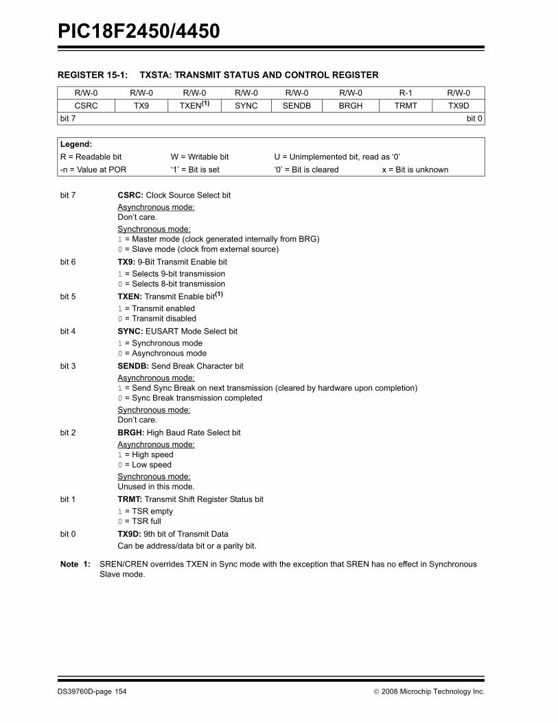
PIC18F2450/4450
DS39760D-page 154 © 2008 Microchip Technology Inc.
REGISTER 15-1: TXSTA: TRANSMIT STATUS AND CONTROL REGISTER
R/W-0 R/W-0 R/W-0 R/W-0 R/W-0 R/W-0 R-1 R/W-0CSRC TX9 TXEN(1) SYNC SENDB BRGH TRMT TX9D
bit 7 bit 0
Legend:R = Readable bit W = Writable bit U = Unimplemented bit, read as �0�-n = Value at POR �1� = Bit is set �0� = Bit is cleared x = Bit is unknown
bit 7 CSRC: Clock Source Select bitAsynchronous mode: Don�t care.Synchronous mode: 1 = Master mode (clock generated internally from BRG)0 = Slave mode (clock from external source)
bit 6 TX9: 9-Bit Transmit Enable bit 1 = Selects 9-bit transmission 0 = Selects 8-bit transmission
bit 5 TXEN: Transmit Enable bit(1)
1 = Transmit enabled0 = Transmit disabled
bit 4 SYNC: EUSART Mode Select bit 1 = Synchronous mode 0 = Asynchronous mode
bit 3 SENDB: Send Break Character bitAsynchronous mode:1 = Send Sync Break on next transmission (cleared by hardware upon completion)0 = Sync Break transmission completedSynchronous mode:Don�t care.
bit 2 BRGH: High Baud Rate Select bit Asynchronous mode: 1 = High speed 0 = Low speedSynchronous mode: Unused in this mode.
bit 1 TRMT: Transmit Shift Register Status bit1 = TSR empty 0 = TSR full
bit 0 TX9D: 9th bit of Transmit DataCan be address/data bit or a parity bit.
Note 1: SREN/CREN overrides TXEN in Sync mode with the exception that SREN has no effect in Synchronous Slave mode.
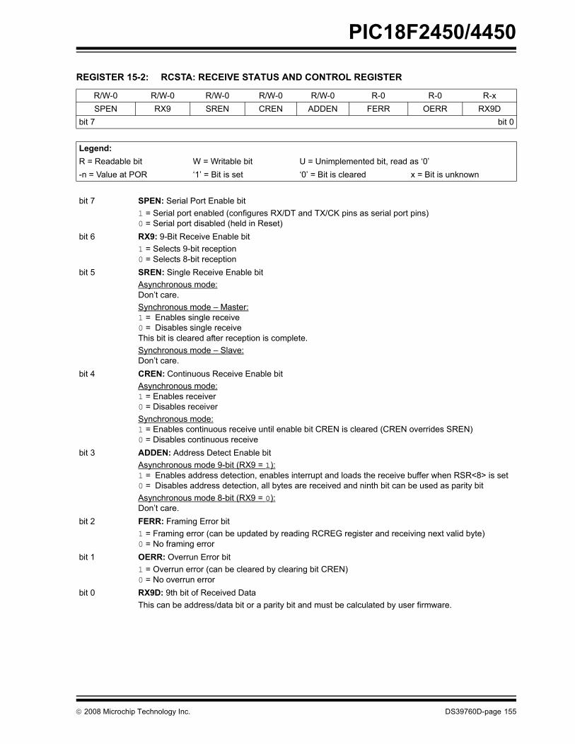
PIC18F2450/4450
© 2008 Microchip Technology Inc. DS39760D-page 155
REGISTER 15-2: RCSTA: RECEIVE STATUS AND CONTROL REGISTER
R/W-0 R/W-0 R/W-0 R/W-0 R/W-0 R-0 R-0 R-xSPEN RX9 SREN CREN ADDEN FERR OERR RX9D
bit 7 bit 0
Legend:R = Readable bit W = Writable bit U = Unimplemented bit, read as �0�-n = Value at POR �1� = Bit is set �0� = Bit is cleared x = Bit is unknown
bit 7 SPEN: Serial Port Enable bit1 = Serial port enabled (configures RX/DT and TX/CK pins as serial port pins)0 = Serial port disabled (held in Reset)
bit 6 RX9: 9-Bit Receive Enable bit1 = Selects 9-bit reception 0 = Selects 8-bit reception
bit 5 SREN: Single Receive Enable bit Asynchronous mode: Don�t care.Synchronous mode � Master: 1 = Enables single receive0 = Disables single receive This bit is cleared after reception is complete.Synchronous mode � Slave: Don�t care.
bit 4 CREN: Continuous Receive Enable bit Asynchronous mode: 1 = Enables receiver0 = Disables receiverSynchronous mode: 1 = Enables continuous receive until enable bit CREN is cleared (CREN overrides SREN) 0 = Disables continuous receive
bit 3 ADDEN: Address Detect Enable bitAsynchronous mode 9-bit (RX9 = 1):1 = Enables address detection, enables interrupt and loads the receive buffer when RSR<8> is set0 = Disables address detection, all bytes are received and ninth bit can be used as parity bitAsynchronous mode 8-bit (RX9 = 0):Don�t care.
bit 2 FERR: Framing Error bit 1 = Framing error (can be updated by reading RCREG register and receiving next valid byte)0 = No framing error
bit 1 OERR: Overrun Error bit 1 = Overrun error (can be cleared by clearing bit CREN) 0 = No overrun error
bit 0 RX9D: 9th bit of Received Data This can be address/data bit or a parity bit and must be calculated by user firmware.

PIC18F2450/4450
DS39760D-page 156 © 2008 Microchip Technology Inc.
REGISTER 15-3: BAUDCON: BAUD RATE CONTROL REGISTER
R/W-0 R-1 U-0 R/W-0 R/W-0 U-0 R/W-0 R/W-0ABDOVF RCIDL � SCKP BRG16 � WUE ABDEN
bit 7 bit 0
Legend:R = Readable bit W = Writable bit U = Unimplemented bit, read as �0�-n = Value at POR �1� = Bit is set �0� = Bit is cleared x = Bit is unknown
bit 7 ABDOVF: Auto-Baud Acquisition Rollover Status bit1 = A BRG rollover has occurred during Auto-Baud Rate Detect mode (must be cleared in software)0 = No BRG rollover has occurred
bit 6 RCIDL: Receive Operation Idle Status bit1 = Receive operation is Idle0 = Receive operation is active
bit 5 Unimplemented: Read as �0�bit 4 SCKP: Synchronous Clock Polarity Select bit
Asynchronous mode:Unused in this mode.Synchronous mode:1 = Idle state for clock (CK) is a high level0 = Idle state for clock (CK) is a low level
bit 3 BRG16: 16-Bit Baud Rate Register Enable bit1 = 16-bit Baud Rate Generator � SPBRGH and SPBRG0 = 8-bit Baud Rate Generator � SPBRG only (Compatible mode), SPBRGH value ignored
bit 2 Unimplemented: Read as �0�bit 1 WUE: Wake-up Enable bit
Asynchronous mode:1 = EUSART will continue to sample the RX pin � interrupt generated on falling edge; bit cleared in
hardware on following rising edge0 = RX pin not monitored or rising edge detectedSynchronous mode:Unused in this mode.
bit 0 ABDEN: Auto-Baud Detect Enable bitAsynchronous mode:1 = Enable baud rate measurement on the next character. Requires reception of a Sync field (55h);
cleared in hardware upon completion.0 = Baud rate measurement disabled or completedSynchronous mode:Unused in this mode.
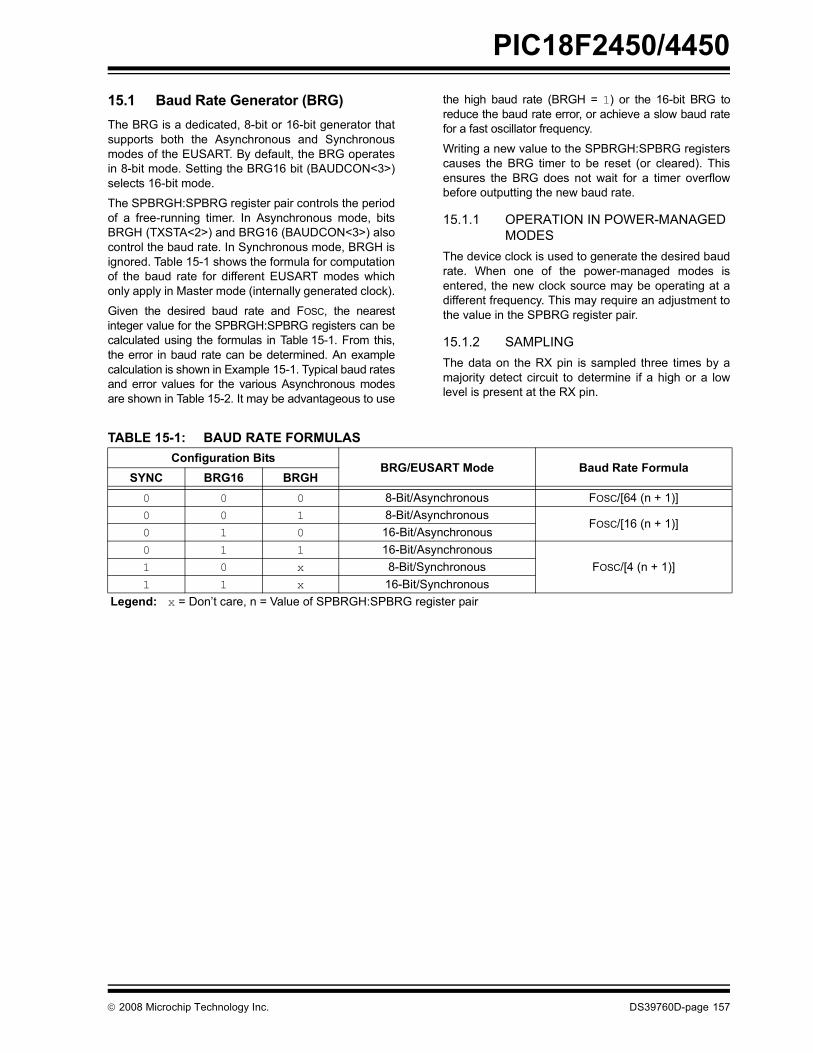
PIC18F2450/4450
© 2008 Microchip Technology Inc. DS39760D-page 157
15.1 Baud Rate Generator (BRG)The BRG is a dedicated, 8-bit or 16-bit generator thatsupports both the Asynchronous and Synchronousmodes of the EUSART. By default, the BRG operatesin 8-bit mode. Setting the BRG16 bit (BAUDCON<3>)selects 16-bit mode.
The SPBRGH:SPBRG register pair controls the periodof a free-running timer. In Asynchronous mode, bitsBRGH (TXSTA<2>) and BRG16 (BAUDCON<3>) alsocontrol the baud rate. In Synchronous mode, BRGH isignored. Table 15-1 shows the formula for computationof the baud rate for different EUSART modes whichonly apply in Master mode (internally generated clock).
Given the desired baud rate and FOSC, the nearestinteger value for the SPBRGH:SPBRG registers can becalculated using the formulas in Table 15-1. From this,the error in baud rate can be determined. An examplecalculation is shown in Example 15-1. Typical baud ratesand error values for the various Asynchronous modesare shown in Table 15-2. It may be advantageous to use
the high baud rate (BRGH = 1) or the 16-bit BRG toreduce the baud rate error, or achieve a slow baud ratefor a fast oscillator frequency.
Writing a new value to the SPBRGH:SPBRG registerscauses the BRG timer to be reset (or cleared). Thisensures the BRG does not wait for a timer overflowbefore outputting the new baud rate.
15.1.1 OPERATION IN POWER-MANAGED MODES
The device clock is used to generate the desired baudrate. When one of the power-managed modes isentered, the new clock source may be operating at adifferent frequency. This may require an adjustment tothe value in the SPBRG register pair.
15.1.2 SAMPLINGThe data on the RX pin is sampled three times by amajority detect circuit to determine if a high or a lowlevel is present at the RX pin.
TABLE 15-1: BAUD RATE FORMULASConfiguration Bits
BRG/EUSART Mode Baud Rate FormulaSYNC BRG16 BRGH0 0 0 8-Bit/Asynchronous FOSC/[64 (n + 1)]0 0 1 8-Bit/Asynchronous
FOSC/[16 (n + 1)]0 1 0 16-Bit/Asynchronous0 1 1 16-Bit/Asynchronous
FOSC/[4 (n + 1)]1 0 x 8-Bit/Synchronous1 1 x 16-Bit/Synchronous
Legend: x = Don�t care, n = Value of SPBRGH:SPBRG register pair
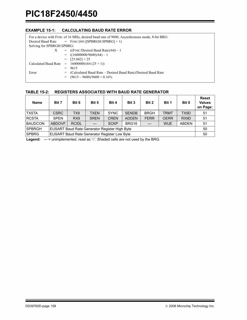
PIC18F2450/4450
DS39760D-page 158 © 2008 Microchip Technology Inc.
EXAMPLE 15-1: CALCULATING BAUD RATE ERROR
TABLE 15-2: REGISTERS ASSOCIATED WITH BAUD RATE GENERATOR
Name Bit 7 Bit 6 Bit 5 Bit 4 Bit 3 Bit 2 Bit 1 Bit 0Reset Values
on Page:TXSTA CSRC TX9 TXEN SYNC SENDB BRGH TRMT TX9D 51RCSTA SPEN RX9 SREN CREN ADDEN FERR OERR RX9D 51BAUDCON ABDOVF RCIDL � SCKP BRG16 � WUE ABDEN 51SPBRGH EUSART Baud Rate Generator Register High Byte 50SPBRG EUSART Baud Rate Generator Register Low Byte 50Legend: � = unimplemented, read as �0�. Shaded cells are not used by the BRG.
For a device with FOSC of 16 MHz, desired baud rate of 9600, Asynchronous mode, 8-bit BRG:Desired Baud Rate = FOSC/(64 ([SPBRGH:SPBRG] + 1) Solving for SPBRGH:SPBRG:
X = ((FOSC/Desired Baud Rate)/64) � 1= ((16000000/9600)/64) � 1 = [25.042] = 25
Calculated Baud Rate = 16000000/(64 (25 + 1)) = 9615
Error = (Calculated Baud Rate � Desired Baud Rate)/Desired Baud Rate= (9615 � 9600)/9600 = 0.16%

PIC18F2450/4450
© 2008 Microchip Technology Inc. DS39760D-page 159
TABLE 15-3: BAUD RATES FOR ASYNCHRONOUS MODES
BAUDRATE
(K)
SYNC = 0, BRGH = 0, BRG16 = 0
FOSC = 40.000 MHz FOSC = 20.000 MHz FOSC = 10.000 MHz FOSC = 8.000 MHzActual Rate (K)
%Error
SPBRGvalue
(decimal)
Actual Rate (K)
%Error
SPBRGvalue
(decimal)
Actual Rate (K)
%Error
SPBRGvalue
(decimal)
Actual Rate (K)
%Error
SPBRGvalue
(decimal)
0.3 � � � � � � � � � � � �1.2 � � � 1.221 1.73 255 1.202 0.16 129 1.201 -0.16 1032.4 2.441 1.73 255 2.404 0.16 129 2.404 0.16 64 2.403 -0.16 519.6 9.615 0.16 64 9.766 1.73 31 9.766 1.73 15 9.615 -0.16 12
19.2 19.531 1.73 31 19.531 1.73 15 19.531 1.73 7 � � �57.6 56.818 -1.36 10 62.500 8.51 4 52.083 -9.58 2 � � �115.2 125.000 8.51 4 104.167 -9.58 2 78.125 -32.18 1 � � �
BAUDRATE
(K)
SYNC = 0, BRGH = 0, BRG16 = 0
FOSC = 4.000 MHz FOSC = 2.000 MHz FOSC = 1.000 MHzActual Rate (K)
%Error
SPBRGvalue
(decimal)
Actual Rate (K)
%Error
SPBRGvalue
(decimal)
Actual Rate (K)
%Error
SPBRGvalue
(decimal)
0.3 0.300 0.16 207 0.300 -0.16 103 0.300 -0.16 511.2 1.202 0.16 51 1.201 -0.16 25 1.201 -0.16 122.4 2.404 0.16 25 2.403 -0.16 12 � � �9.6 8.929 -6.99 6 � � � � � �
19.2 20.833 8.51 2 � � � � � �57.6 62.500 8.51 0 � � � � � �115.2 62.500 -45.75 0 � � � � � �
BAUDRATE
(K)
SYNC = 0, BRGH = 1, BRG16 = 0
FOSC = 40.000 MHz FOSC = 20.000 MHz FOSC = 10.000 MHz FOSC = 8.000 MHzActual Rate (K)
%Error
SPBRGvalue
(decimal)
Actual Rate (K)
%Error
SPBRGvalue
(decimal)
Actual Rate (K)
%Error
SPBRGvalue
(decimal)
Actual Rate (K)
%Error
SPBRGvalue
(decimal)
0.3 � � � � � � � � � � � �1.2 � � � � � � � � � � � �2.4 � � � � � � 2.441 1.73 255 2.403 -0.16 2079.6 9.766 1.73 255 9.615 0.16 129 9.615 0.16 64 9.615 -0.16 51
19.2 19.231 0.16 129 19.231 0.16 64 19.531 1.73 31 19.230 -0.16 2557.6 58.140 0.94 42 56.818 -1.36 21 56.818 -1.36 10 55.555 3.55 8115.2 113.636 -1.36 21 113.636 -1.36 10 125.000 8.51 4 � � �
BAUDRATE
(K)
SYNC = 0, BRGH = 1, BRG16 = 0
FOSC = 4.000 MHz FOSC = 2.000 MHz FOSC = 1.000 MHzActual Rate (K)
%Error
SPBRGvalue
(decimal)
Actual Rate (K)
%Error
SPBRGvalue
(decimal)
Actual Rate (K)
%Error
SPBRGvalue
(decimal)
0.3 � � � � � � 0.300 -0.16 2071.2 1.202 0.16 207 1.201 -0.16 103 1.201 -0.16 512.4 2.404 0.16 103 2.403 -0.16 51 2.403 -0.16 259.6 9.615 0.16 25 9.615 -0.16 12 � � �
19.2 19.231 0.16 12 � � � � � �57.6 62.500 8.51 3 � � � � � �115.2 125.000 8.51 1 � � � � � �

PIC18F2450/4450
DS39760D-page 160 © 2008 Microchip Technology Inc.
BAUDRATE
(K)
SYNC = 0, BRGH = 0, BRG16 = 1
FOSC = 40.000 MHz FOSC = 20.000 MHz FOSC = 10.000 MHz FOSC = 8.000 MHzActual Rate (K)
%Error
SPBRGvalue
(decimal)
Actual Rate (K)
%Error
SPBRGvalue
(decimal)
Actual Rate (K)
%Error
SPBRGvalue
(decimal)
Actual Rate (K)
%Error
SPBRGvalue
(decimal)
0.3 0.300 0.00 8332 0.300 0.02 4165 0.300 0.02 2082 0.300 -0.04 16651.2 1.200 0.02 2082 1.200 -0.03 1041 1.200 -0.03 520 1.201 -0.16 4152.4 2.402 0.06 1040 2.399 -0.03 520 2.404 0.16 259 2.403 -0.16 2079.6 9.615 0.16 259 9.615 0.16 129 9.615 0.16 64 9.615 -0.16 51
19.2 19.231 0.16 129 19.231 0.16 64 19.531 1.73 31 19.230 -0.16 2557.6 58.140 0.94 42 56.818 -1.36 21 56.818 -1.36 10 55.555 3.55 8115.2 113.636 -1.36 21 113.636 -1.36 10 125.000 8.51 4 � � �
BAUDRATE
(K)
SYNC = 0, BRGH = 0, BRG16 = 1
FOSC = 4.000 MHz FOSC = 2.000 MHz FOSC = 1.000 MHzActual Rate (K)
%Error
SPBRGvalue
(decimal)
Actual Rate (K)
%Error
SPBRGvalue
(decimal)
Actual Rate (K)
%Error
SPBRGvalue
(decimal)
0.3 0.300 0.04 832 0.300 -0.16 415 0.300 -0.16 2071.2 1.202 0.16 207 1.201 -0.16 103 1.201 -0.16 512.4 2.404 0.16 103 2.403 -0.16 51 2.403 -0.16 259.6 9.615 0.16 25 9.615 -0.16 12 � � �
19.2 19.231 0.16 12 � � � � � �57.6 62.500 8.51 3 � � � � � �115.2 125.000 8.51 1 � � � � � �
BAUDRATE
(K)
SYNC = 0, BRGH = 1, BRG16 = 1 or SYNC = 1, BRG16 = 1
FOSC = 40.000 MHz FOSC = 20.000 MHz FOSC = 10.000 MHz FOSC = 8.000 MHzActual Rate (K)
%Error
SPBRGvalue
(decimal)
Actual Rate (K)
%Error
SPBRGvalue
(decimal)
Actual Rate (K)
%Error
SPBRGvalue
(decimal)
Actual Rate (K)
%Error
SPBRGvalue
(decimal)
0.3 0.300 0.00 33332 0.300 0.00 16665 0.300 0.00 8332 0.300 -0.01 66651.2 1.200 0.00 8332 1.200 0.02 4165 1.200 0.02 2082 1.200 -0.04 16652.4 2.400 0.02 4165 2.400 0.02 2082 2.402 0.06 1040 2.400 -0.04 8329.6 9.606 0.06 1040 9.596 -0.03 520 9.615 0.16 259 9.615 -0.16 207
19.2 19.193 -0.03 520 19.231 0.16 259 19.231 0.16 129 19.230 -0.16 10357.6 57.803 0.35 172 57.471 -0.22 86 58.140 0.94 42 57.142 0.79 34115.2 114.943 -0.22 86 116.279 0.94 42 113.636 -1.36 21 117.647 -2.12 16
BAUDRATE
(K)
SYNC = 0, BRGH = 1, BRG16 = 1 or SYNC = 1, BRG16 = 1
FOSC = 4.000 MHz FOSC = 2.000 MHz FOSC = 1.000 MHzActual Rate (K)
%Error
SPBRGvalue
(decimal)
Actual Rate (K)
%Error
SPBRGvalue
(decimal)
Actual Rate (K)
%Error
SPBRGvalue
(decimal)
0.3 0.300 0.01 3332 0.300 -0.04 1665 0.300 -0.04 8321.2 1.200 0.04 832 1.201 -0.16 415 1.201 -0.16 2072.4 2.404 0.16 415 2.403 -0.16 207 2.403 -0.16 1039.6 9.615 0.16 103 9.615 -0.16 51 9.615 -0.16 25
19.2 19.231 0.16 51 19.230 -0.16 25 19.230 -0.16 1257.6 58.824 2.12 16 55.555 3.55 8 � � �115.2 111.111 -3.55 8 � � � � � �
TABLE 15-3: BAUD RATES FOR ASYNCHRONOUS MODES (CONTINUED)
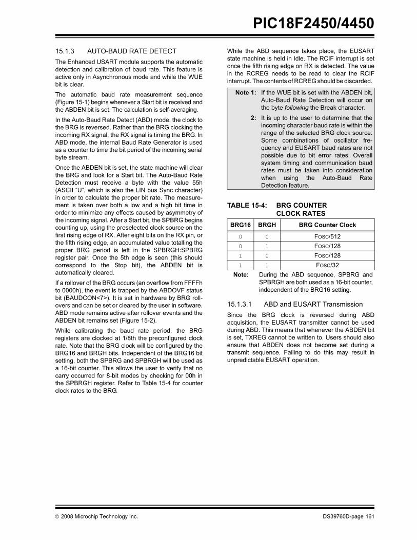
PIC18F2450/4450
© 2008 Microchip Technology Inc. DS39760D-page 161
15.1.3 AUTO-BAUD RATE DETECTThe Enhanced USART module supports the automaticdetection and calibration of baud rate. This feature isactive only in Asynchronous mode and while the WUEbit is clear.
The automatic baud rate measurement sequence(Figure 15-1) begins whenever a Start bit is received andthe ABDEN bit is set. The calculation is self-averaging.
In the Auto-Baud Rate Detect (ABD) mode, the clock tothe BRG is reversed. Rather than the BRG clocking theincoming RX signal, the RX signal is timing the BRG. InABD mode, the internal Baud Rate Generator is usedas a counter to time the bit period of the incoming serialbyte stream.
Once the ABDEN bit is set, the state machine will clearthe BRG and look for a Start bit. The Auto-Baud RateDetection must receive a byte with the value 55h(ASCII �U�, which is also the LIN bus Sync character)in order to calculate the proper bit rate. The measure-ment is taken over both a low and a high bit time inorder to minimize any effects caused by asymmetry ofthe incoming signal. After a Start bit, the SPBRG beginscounting up, using the preselected clock source on thefirst rising edge of RX. After eight bits on the RX pin, orthe fifth rising edge, an accumulated value totalling theproper BRG period is left in the SPBRGH:SPBRGregister pair. Once the 5th edge is seen (this shouldcorrespond to the Stop bit), the ABDEN bit isautomatically cleared.
If a rollover of the BRG occurs (an overflow from FFFFhto 0000h), the event is trapped by the ABDOVF statusbit (BAUDCON<7>). It is set in hardware by BRG roll-overs and can be set or cleared by the user in software.ABD mode remains active after rollover events and theABDEN bit remains set (Figure 15-2).
While calibrating the baud rate period, the BRGregisters are clocked at 1/8th the preconfigured clockrate. Note that the BRG clock will be configured by theBRG16 and BRGH bits. Independent of the BRG16 bitsetting, both the SPBRG and SPBRGH will be used asa 16-bit counter. This allows the user to verify that nocarry occurred for 8-bit modes by checking for 00h inthe SPBRGH register. Refer to Table 15-4 for counterclock rates to the BRG.
While the ABD sequence takes place, the EUSARTstate machine is held in Idle. The RCIF interrupt is setonce the fifth rising edge on RX is detected. The valuein the RCREG needs to be read to clear the RCIFinterrupt. The contents of RCREG should be discarded.
TABLE 15-4: BRG COUNTER CLOCK RATES
15.1.3.1 ABD and EUSART TransmissionSince the BRG clock is reversed during ABDacquisition, the EUSART transmitter cannot be usedduring ABD. This means that whenever the ABDEN bitis set, TXREG cannot be written to. Users should alsoensure that ABDEN does not become set during atransmit sequence. Failing to do this may result inunpredictable EUSART operation.
Note 1: If the WUE bit is set with the ABDEN bit,Auto-Baud Rate Detection will occur onthe byte following the Break character.
2: It is up to the user to determine that theincoming character baud rate is within therange of the selected BRG clock source.Some combinations of oscillator fre-quency and EUSART baud rates are notpossible due to bit error rates. Overallsystem timing and communication baudrates must be taken into considerationwhen using the Auto-Baud RateDetection feature.
BRG16 BRGH BRG Counter Clock
0 0 FOSC/5120 1 FOSC/1281 0 FOSC/1281 1 FOSC/32
Note: During the ABD sequence, SPBRG andSPBRGH are both used as a 16-bit counter,independent of the BRG16 setting.
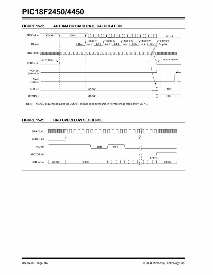
PIC18F2450/4450
DS39760D-page 162 © 2008 Microchip Technology Inc.
FIGURE 15-1: AUTOMATIC BAUD RATE CALCULATION
FIGURE 15-2: BRG OVERFLOW SEQUENCE
BRG Value
RX pin
ABDEN bit
RCIF bit
bit 0 bit 1
(Interrupt)
ReadRCREG
BRG Clock
Start
Auto-ClearedSet by User
XXXXh 0000h
Edge #1bit 2 bit 3Edge #2
bit 4 bit 5Edge #3
bit 6 bit 7Edge #4 Edge #5
001Ch
Note: The ABD sequence requires the EUSART module to be configured in Asynchronous mode and WUE = 0.
SPBRG XXXXh 1Ch
SPBRGH XXXXh 00h
Stop bit
Start bit 0
XXXXh 0000h 0000hFFFFh
BRG Clock
ABDEN bit
RX pin
ABDOVF bit
BRG Value
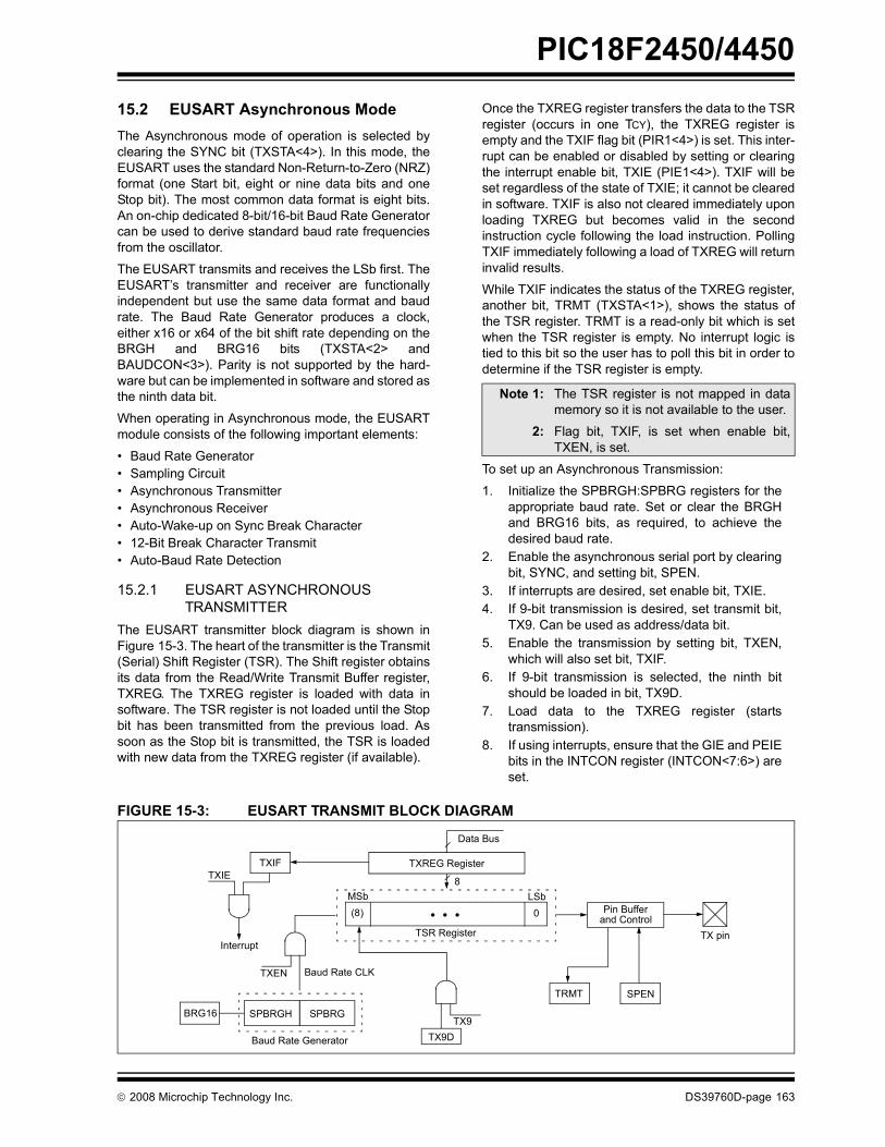
PIC18F2450/4450
© 2008 Microchip Technology Inc. DS39760D-page 163
15.2 EUSART Asynchronous ModeThe Asynchronous mode of operation is selected byclearing the SYNC bit (TXSTA<4>). In this mode, theEUSART uses the standard Non-Return-to-Zero (NRZ)format (one Start bit, eight or nine data bits and oneStop bit). The most common data format is eight bits.An on-chip dedicated 8-bit/16-bit Baud Rate Generatorcan be used to derive standard baud rate frequenciesfrom the oscillator.
The EUSART transmits and receives the LSb first. TheEUSART�s transmitter and receiver are functionallyindependent but use the same data format and baudrate. The Baud Rate Generator produces a clock,either x16 or x64 of the bit shift rate depending on theBRGH and BRG16 bits (TXSTA<2> andBAUDCON<3>). Parity is not supported by the hard-ware but can be implemented in software and stored asthe ninth data bit.
When operating in Asynchronous mode, the EUSARTmodule consists of the following important elements:
� Baud Rate Generator� Sampling Circuit� Asynchronous Transmitter� Asynchronous Receiver� Auto-Wake-up on Sync Break Character� 12-Bit Break Character Transmit� Auto-Baud Rate Detection
15.2.1 EUSART ASYNCHRONOUS TRANSMITTER
The EUSART transmitter block diagram is shown inFigure 15-3. The heart of the transmitter is the Transmit(Serial) Shift Register (TSR). The Shift register obtainsits data from the Read/Write Transmit Buffer register,TXREG. The TXREG register is loaded with data insoftware. The TSR register is not loaded until the Stopbit has been transmitted from the previous load. Assoon as the Stop bit is transmitted, the TSR is loadedwith new data from the TXREG register (if available).
Once the TXREG register transfers the data to the TSRregister (occurs in one TCY), the TXREG register isempty and the TXIF flag bit (PIR1<4>) is set. This inter-rupt can be enabled or disabled by setting or clearingthe interrupt enable bit, TXIE (PIE1<4>). TXIF will beset regardless of the state of TXIE; it cannot be clearedin software. TXIF is also not cleared immediately uponloading TXREG but becomes valid in the secondinstruction cycle following the load instruction. PollingTXIF immediately following a load of TXREG will returninvalid results.
While TXIF indicates the status of the TXREG register,another bit, TRMT (TXSTA<1>), shows the status ofthe TSR register. TRMT is a read-only bit which is setwhen the TSR register is empty. No interrupt logic istied to this bit so the user has to poll this bit in order todetermine if the TSR register is empty.
To set up an Asynchronous Transmission:
1. Initialize the SPBRGH:SPBRG registers for theappropriate baud rate. Set or clear the BRGHand BRG16 bits, as required, to achieve thedesired baud rate.
2. Enable the asynchronous serial port by clearingbit, SYNC, and setting bit, SPEN.
3. If interrupts are desired, set enable bit, TXIE.4. If 9-bit transmission is desired, set transmit bit,
TX9. Can be used as address/data bit.5. Enable the transmission by setting bit, TXEN,
which will also set bit, TXIF.6. If 9-bit transmission is selected, the ninth bit
should be loaded in bit, TX9D.7. Load data to the TXREG register (starts
transmission).8. If using interrupts, ensure that the GIE and PEIE
bits in the INTCON register (INTCON<7:6>) areset.
FIGURE 15-3: EUSART TRANSMIT BLOCK DIAGRAM
Note 1: The TSR register is not mapped in datamemory so it is not available to the user.
2: Flag bit, TXIF, is set when enable bit,TXEN, is set.
TXIFTXIE
Interrupt
TXEN Baud Rate CLK
SPBRG
Baud Rate Generator
MSb LSb
Data Bus
TXREG Register
TSR Register
(8) 0
TX9
TRMT SPEN
TX pin
Pin Bufferand Control
8
• • •
SPBRGHBRG16
TX9D

PIC18F2450/4450
DS39760D-page 164 © 2008 Microchip Technology Inc.
FIGURE 15-4: ASYNCHRONOUS TRANSMISSION
FIGURE 15-5: ASYNCHRONOUS TRANSMISSION (BACK-TO-BACK)
TABLE 15-5: REGISTERS ASSOCIATED WITH ASYNCHRONOUS TRANSMISSION
Name Bit 7 Bit 6 Bit 5 Bit 4 Bit 3 Bit 2 Bit 1 Bit 0Reset
Values on Page:
INTCON GIE/GIEH PEIE/GIEL TMR0IE INT0IE RBIE TMR0IF INT0IF RBIF 49PIR1 � ADIF RCIF TXIF � CCP1IF TMR2IF TMR1IF 51PIE1 � ADIE RCIE TXIE � CCP1IE TMR2IE TMR1IE 51IPR1 � ADIP RCIP TXIP � CCP1IP TMR2IP TMR1IP 51RCSTA SPEN RX9 SREN CREN ADDEN FERR OERR RX9D 51TXREG EUSART Transmit Register 51TXSTA CSRC TX9 TXEN SYNC SENDB BRGH TRMT TX9D 51BAUDCON ABDOVF RCIDL � SCKP BRG16 � WUE ABDEN 51SPBRGH EUSART Baud Rate Generator Register High Byte 50SPBRG EUSART Baud Rate Generator Register Low Byte 50Legend: � = unimplemented locations read as �0�. Shaded cells are not used for asynchronous transmission.
Word 1
Word 1Transmit Shift Reg
Start bit bit 0 bit 1 bit 7/8
Write to TXREG
BRG Output(Shift Clock)
TX
TXIF bit(Transmit Buffer
Reg. Empty Flag)
TRMT bit(Transmit Shift
Reg. Empty Flag)
1 TCY
(pin)
Word 1
Stop bit
Transmit Shift Reg.
Write to TXREG
BRG Output(Shift Clock)
TX
TXIF bit(Interrupt Reg. Flag)
TRMT bit(Transmit Shift
Reg. Empty Flag)
Word 1 Word 2
Word 1 Word 2
Stop bit Start bit
Transmit Shift Reg.
Word 1 Word 2
bit 0 bit 1 bit 7/8 bit 0
Note: This timing diagram shows two consecutive transmissions.
1 TCY
1 TCY
(pin) Start bit
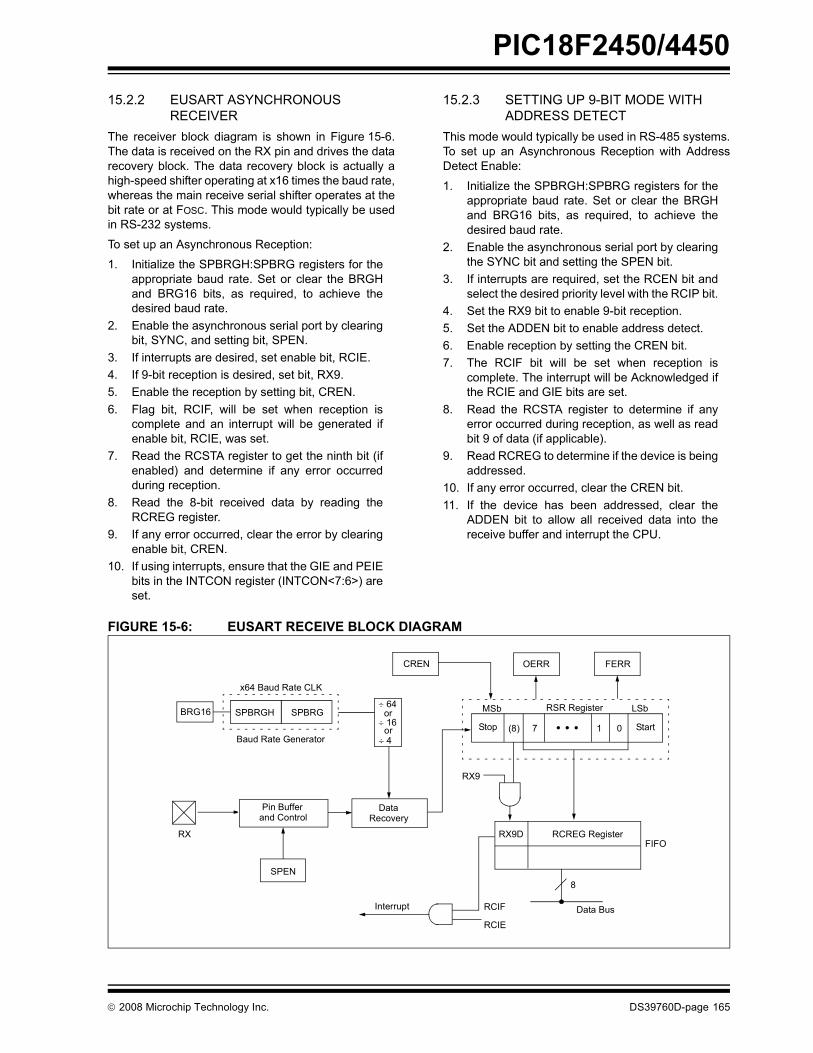
PIC18F2450/4450
© 2008 Microchip Technology Inc. DS39760D-page 165
15.2.2 EUSART ASYNCHRONOUS RECEIVER
The receiver block diagram is shown in Figure 15-6.The data is received on the RX pin and drives the datarecovery block. The data recovery block is actually ahigh-speed shifter operating at x16 times the baud rate,whereas the main receive serial shifter operates at thebit rate or at FOSC. This mode would typically be usedin RS-232 systems.
To set up an Asynchronous Reception:
1. Initialize the SPBRGH:SPBRG registers for theappropriate baud rate. Set or clear the BRGHand BRG16 bits, as required, to achieve thedesired baud rate.
2. Enable the asynchronous serial port by clearingbit, SYNC, and setting bit, SPEN.
3. If interrupts are desired, set enable bit, RCIE.4. If 9-bit reception is desired, set bit, RX9.5. Enable the reception by setting bit, CREN.6. Flag bit, RCIF, will be set when reception is
complete and an interrupt will be generated ifenable bit, RCIE, was set.
7. Read the RCSTA register to get the ninth bit (ifenabled) and determine if any error occurredduring reception.
8. Read the 8-bit received data by reading theRCREG register.
9. If any error occurred, clear the error by clearingenable bit, CREN.
10. If using interrupts, ensure that the GIE and PEIEbits in the INTCON register (INTCON<7:6>) areset.
15.2.3 SETTING UP 9-BIT MODE WITH ADDRESS DETECT
This mode would typically be used in RS-485 systems.To set up an Asynchronous Reception with AddressDetect Enable:
1. Initialize the SPBRGH:SPBRG registers for theappropriate baud rate. Set or clear the BRGHand BRG16 bits, as required, to achieve thedesired baud rate.
2. Enable the asynchronous serial port by clearingthe SYNC bit and setting the SPEN bit.
3. If interrupts are required, set the RCEN bit andselect the desired priority level with the RCIP bit.
4. Set the RX9 bit to enable 9-bit reception. 5. Set the ADDEN bit to enable address detect.6. Enable reception by setting the CREN bit.7. The RCIF bit will be set when reception is
complete. The interrupt will be Acknowledged ifthe RCIE and GIE bits are set.
8. Read the RCSTA register to determine if anyerror occurred during reception, as well as readbit 9 of data (if applicable).
9. Read RCREG to determine if the device is beingaddressed.
10. If any error occurred, clear the CREN bit. 11. If the device has been addressed, clear the
ADDEN bit to allow all received data into thereceive buffer and interrupt the CPU.
FIGURE 15-6: EUSART RECEIVE BLOCK DIAGRAM
x64 Baud Rate CLK
Baud Rate Generator
RX
Pin Bufferand Control
SPEN
DataRecovery
CREN OERR FERR
RSR RegisterMSb LSb
RX9D RCREG RegisterFIFO
Interrupt RCIF
RCIEData Bus
8
÷ 64
÷ 16or
Stop Start(8) 7 1 0
RX9
• • •
SPBRGSPBRGHBRG16
or÷ 4

PIC18F2450/4450
DS39760D-page 166 © 2008 Microchip Technology Inc.
FIGURE 15-7: ASYNCHRONOUS RECEPTION
TABLE 15-6: REGISTERS ASSOCIATED WITH ASYNCHRONOUS RECEPTION
Name Bit 7 Bit 6 Bit 5 Bit 4 Bit 3 Bit 2 Bit 1 Bit 0Reset Values
on Page:
INTCON GIE/GIEH PEIE/GIEL TMR0IE INT0IE RBIE TMR0IF INT0IF RBIF 49PIR1 � ADIF RCIF TXIF � CCP1IF TMR2IF TMR1IF 51PIE1 � ADIE RCIE TXIE � CCP1IE TMR2IE TMR1IE 51IPR1 � ADIP RCIP TXIP � CCP1IP TMR2IP TMR1IP 51RCSTA SPEN RX9 SREN CREN ADDEN FERR OERR RX9D 51RCREG EUSART Receive Register 50TXSTA CSRC TX9 TXEN SYNC SENDB BRGH TRMT TX9D 51BAUDCON ABDOVF RCIDL � SCKP BRG16 � WUE ABDEN 51SPBRGH EUSART Baud Rate Generator Register High Byte 50SPBRG EUSART Baud Rate Generator Register Low Byte 50Legend: � = unimplemented locations read as �0�. Shaded cells are not used for asynchronous reception.
Startbit bit 7/8bit 1bit 0 bit 7/8 bit 0Stop
bit
Startbit
Startbitbit 7/8 Stop
bitRX (pin)
Rcv Buffer RegRcv Shift Reg
Read RcvBuffer RegRCREG
RCIF(Interrupt Flag)
OERR bit
CREN
Word 1RCREG
Word 2RCREG
Stopbit
Note: This timing diagram shows three words appearing on the RX input. The RCREG (Receive Buffer) is read after the third wordcausing the OERR (Overrun Error) bit to be set.
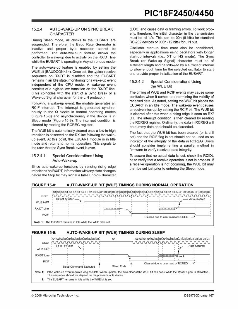
PIC18F2450/4450
© 2008 Microchip Technology Inc. DS39760D-page 167
15.2.4 AUTO-WAKE-UP ON SYNC BREAK CHARACTER
During Sleep mode, all clocks to the EUSART aresuspended. Therefore, the Baud Rate Generator isinactive and proper byte reception cannot beperformed. The auto-wake-up feature allows thecontroller to wake-up due to activity on the RX/DT linewhile the EUSART is operating in Asynchronous mode.
The auto-wake-up feature is enabled by setting theWUE bit (BAUDCON<1>). Once set, the typical receivesequence on RX/DT is disabled and the EUSARTremains in an Idle state, monitoring for a wake-up eventindependent of the CPU mode. A wake-up eventconsists of a high-to-low transition on the RX/DT line.(This coincides with the start of a Sync Break or aWake-up Signal character for the LIN protocol.)
Following a wake-up event, the module generates anRCIF interrupt. The interrupt is generated synchro-nously to the Q clocks in normal operating modes(Figure 15-8) and asynchronously if the device is inSleep mode (Figure 15-9). The interrupt condition iscleared by reading the RCREG register.
The WUE bit is automatically cleared once a low-to-hightransition is observed on the RX line following the wake-up event. At this point, the EUSART module is in Idlemode and returns to normal operation. This signals tothe user that the Sync Break event is over.
15.2.4.1 Special Considerations Using Auto-Wake-up
Since auto-wake-up functions by sensing rising edgetransitions on RX/DT, information with any state changesbefore the Stop bit may signal a false End-of-Character
(EOC) and cause data or framing errors. To work prop-erly, therefore, the initial character in the transmissionmust be all �0�s. This can be 00h (8 bits) for standardRS-232 devices or 000h (12 bits) for LIN bus.
Oscillator start-up time must also be considered,especially in applications using oscillators with longerstart-up intervals (i.e., XT or HS mode). The SyncBreak (or Wake-up Signal) character must be ofsufficient length and be followed by a sufficient intervalto allow enough time for the selected oscillator to startand provide proper initialization of the EUSART.
15.2.4.2 Special Considerations Using the WUE Bit
The timing of WUE and RCIF events may cause someconfusion when it comes to determining the validity ofreceived data. As noted, setting the WUE bit places theEUSART in an Idle mode. The wake-up event causesa receive interrupt by setting the RCIF bit. The WUE bitis cleared after this when a rising edge is seen on RX/DT. The interrupt condition is then cleared by readingthe RCREG register. Ordinarily, the data in RCREG willbe dummy data and should be discarded.
The fact that the WUE bit has been cleared (or is stillset) and the RCIF flag is set should not be used as anindicator of the integrity of the data in RCREG. Usersshould consider implementing a parallel method infirmware to verify received data integrity.
To assure that no actual data is lost, check the RCIDLbit to verify that a receive operation is not in process. Ifa receive operation is not occurring, the WUE bit maythen be set just prior to entering the Sleep mode.
FIGURE 15-8: AUTO-WAKE-UP BIT (WUE) TIMINGS DURING NORMAL OPERATION
FIGURE 15-9: AUTO-WAKE-UP BIT (WUE) TIMINGS DURING SLEEP
Q1 Q2 Q3 Q4 Q1 Q2 Q3 Q4 Q1 Q2 Q3 Q4 Q1 Q2 Q3 Q4 Q1 Q2 Q3 Q4 Q1 Q2 Q3 Q4 Q1 Q2 Q3 Q4 Q1 Q2 Q3 Q4 Q1 Q2 Q3 Q4 Q1 Q2 Q3 Q4
OSC1
WUE bit(1)
RX/DT Line
RCIF
Note 1: The EUSART remains in Idle while the WUE bit is set.
Bit set by user Auto-Cleared
Cleared due to user read of RCREG
Q1 Q2 Q3 Q4 Q1 Q2 Q3 Q4 Q1 Q2 Q3 Q4 Q1 Q2 Q3 Q4 Q1 Q2 Q3 Q4 Q1 Q2 Q3 Q4 Q1 Q2 Q3 Q4 Q1 Q2 Q3 Q4
OSC1
WUE bit(2)
RX/DT Line
RCIF
Sleep Command Executed
Note 1: If the wake-up event requires long oscillator warm-up time, the auto-clear of the WUE bit can occur while the stposc signal is still active.This sequence should not depend on the presence of Q clocks.
2: The EUSART remains in Idle while the WUE bit is set.
Sleep Ends
Auto-Cleared
Note 1
Cleared due to user read of RCREG
Bit set by user

PIC18F2450/4450
DS39760D-page 168 © 2008 Microchip Technology Inc.
15.2.5 BREAK CHARACTER SEQUENCEThe EUSART module has the capability of sending thespecial Break character sequences that are required bythe LIN bus standard. The Break character transmitconsists of a Start bit, followed by twelve �0� bits and aStop bit. The Frame Break character is sent wheneverthe SENDB and TXEN bits (TXSTA<3> andTXSTA<5>) are set while the Transmit Shift Register isloaded with data. Note that the value of data written toTXREG will be ignored and all �0�s will be transmitted.
The SENDB bit is automatically reset by hardware afterthe corresponding Stop bit is sent. This allows the userto preload the transmit FIFO with the next transmit bytefollowing the Break character (typically, the Synccharacter in the LIN specification).
Note that the data value written to the TXREG for theBreak character is ignored. The write simply serves thepurpose of initiating the proper sequence.
The TRMT bit indicates when the transmit operation isactive or Idle, just as it does during normal transmission.See Figure 15-10 for the timing of the Break charactersequence.
15.2.5.1 Break and Sync Transmit SequenceThe following sequence will send a message frameheader made up of a Break, followed by an Auto-BaudSync byte. This sequence is typical of a LIN bus master.
1. Configure the EUSART for the desired mode.2. Set the TXEN and SENDB bits to set up the
Break character.
3. Load the TXREG with a dummy character toinitiate transmission (the value is ignored).
4. Write �55h� to TXREG to load the Sync characterinto the transmit FIFO buffer.
5. After the Break has been sent, the SENDB bit isreset by hardware. The Sync character nowtransmits in the preconfigured mode.
When the TXREG becomes empty, as indicated by theTXIF, the next data byte can be written to TXREG.
15.2.6 RECEIVING A BREAK CHARACTERThe Enhanced USART module can receive a Breakcharacter in two ways.
The first method forces configuration of the baud rateat a frequency of 9/13 the typical speed. This allows forthe Stop bit transition to be at the correct samplinglocation (13 bits for Break versus Start bit and eightdata bits for typical data).
The second method uses the auto-wake-up featuredescribed in Section 15.2.4 �Auto-Wake-up on SyncBreak Character�. By enabling this feature, theEUSART will sample the next two transitions on RX/DT,cause an RCIF interrupt and receive the next data bytefollowed by another interrupt.
Note that following a Break character, the user willtypically want to enable the Auto-Baud Rate Detectfeature. For both methods, the user can set the ABD bitonce the TXIF interrupt is observed.
FIGURE 15-10: SEND BREAK CHARACTER SEQUENCE
Write to TXREG
BRG Output(Shift Clock)
Start bit bit 0 bit 1 bit 11 Stop bit
Break
TXIF bit(Transmit Buffer
Reg. Empty Flag)
TX (pin)
TRMT bit(Transmit Shift
Reg. Empty Flag)
SENDB(Transmit Shift
Reg. Empty Flag)
SENDB sampled here Auto-Cleared
Dummy Write
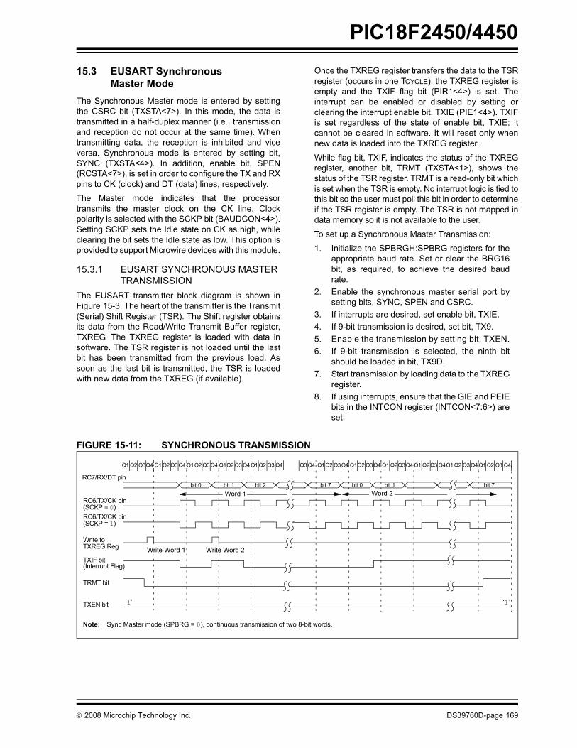
PIC18F2450/4450
© 2008 Microchip Technology Inc. DS39760D-page 169
15.3 EUSART Synchronous Master Mode
The Synchronous Master mode is entered by settingthe CSRC bit (TXSTA<7>). In this mode, the data istransmitted in a half-duplex manner (i.e., transmissionand reception do not occur at the same time). Whentransmitting data, the reception is inhibited and viceversa. Synchronous mode is entered by setting bit,SYNC (TXSTA<4>). In addition, enable bit, SPEN(RCSTA<7>), is set in order to configure the TX and RXpins to CK (clock) and DT (data) lines, respectively.
The Master mode indicates that the processortransmits the master clock on the CK line. Clockpolarity is selected with the SCKP bit (BAUDCON<4>).Setting SCKP sets the Idle state on CK as high, whileclearing the bit sets the Idle state as low. This option isprovided to support Microwire devices with this module.
15.3.1 EUSART SYNCHRONOUS MASTER TRANSMISSION
The EUSART transmitter block diagram is shown inFigure 15-3. The heart of the transmitter is the Transmit(Serial) Shift Register (TSR). The Shift register obtainsits data from the Read/Write Transmit Buffer register,TXREG. The TXREG register is loaded with data insoftware. The TSR register is not loaded until the lastbit has been transmitted from the previous load. Assoon as the last bit is transmitted, the TSR is loadedwith new data from the TXREG (if available).
Once the TXREG register transfers the data to the TSRregister (occurs in one TCYCLE), the TXREG register isempty and the TXIF flag bit (PIR1<4>) is set. Theinterrupt can be enabled or disabled by setting orclearing the interrupt enable bit, TXIE (PIE1<4>). TXIFis set regardless of the state of enable bit, TXIE; itcannot be cleared in software. It will reset only whennew data is loaded into the TXREG register.
While flag bit, TXIF, indicates the status of the TXREGregister, another bit, TRMT (TXSTA<1>), shows thestatus of the TSR register. TRMT is a read-only bit whichis set when the TSR is empty. No interrupt logic is tied tothis bit so the user must poll this bit in order to determineif the TSR register is empty. The TSR is not mapped indata memory so it is not available to the user.
To set up a Synchronous Master Transmission:
1. Initialize the SPBRGH:SPBRG registers for theappropriate baud rate. Set or clear the BRG16bit, as required, to achieve the desired baudrate.
2. Enable the synchronous master serial port bysetting bits, SYNC, SPEN and CSRC.
3. If interrupts are desired, set enable bit, TXIE.4. If 9-bit transmission is desired, set bit, TX9.5. Enable the transmission by setting bit, TXEN.6. If 9-bit transmission is selected, the ninth bit
should be loaded in bit, TX9D.7. Start transmission by loading data to the TXREG
register.8. If using interrupts, ensure that the GIE and PEIE
bits in the INTCON register (INTCON<7:6>) areset.
FIGURE 15-11: SYNCHRONOUS TRANSMISSION
bit 0 bit 1 bit 7Word 1
Q1 Q2 Q3Q4 Q1 Q2 Q3 Q4 Q1Q2 Q3 Q4 Q1Q2 Q3 Q4 Q1 Q2 Q3 Q4 Q3 Q4 Q1 Q2 Q3Q4 Q1Q2 Q3Q4 Q1 Q2Q3Q4 Q1 Q2Q3 Q4Q1 Q2 Q3 Q4 Q1 Q2 Q3 Q4
bit 2 bit 0 bit 1 bit 7RC7/RX/DT pin
RC6/TX/CK pin
Write toTXREG Reg
TXIF bit(Interrupt Flag)
TXEN bit �1� �1�
Word 2
TRMT bit
Write Word 1 Write Word 2
Note: Sync Master mode (SPBRG = 0), continuous transmission of two 8-bit words.
RC6/TX/CK pin(SCKP = 0)
(SCKP = 1)

PIC18F2450/4450
DS39760D-page 170 © 2008 Microchip Technology Inc.
FIGURE 15-12: SYNCHRONOUS TRANSMISSION (THROUGH TXEN)
TABLE 15-7: REGISTERS ASSOCIATED WITH SYNCHRONOUS MASTER TRANSMISSION
Name Bit 7 Bit 6 Bit 5 Bit 4 Bit 3 Bit 2 Bit 1 Bit 0Reset Values
on Page:
INTCON GIE/GIEH PEIE/GIEL TMR0IE INT0IE RBIE TMR0IF INT0IF RBIF 49PIR1 � ADIF RCIF TXIF � CCP1IF TMR2IF TMR1IF 51PIE1 � ADIE RCIE TXIE � CCP1IE TMR2IE TMR1IE 51IPR1 � ADIP RCIP TXIP � CCP1IP TMR2IP TMR1IP 51RCSTA SPEN RX9 SREN CREN ADDEN FERR OERR RX9D 51TXREG EUSART Transmit Register 51TXSTA CSRC TX9 TXEN SYNC SENDB BRGH TRMT TX9D 51BAUDCON ABDOVF RCIDL � SCKP BRG16 � WUE ABDEN 51SPBRGH EUSART Baud Rate Generator Register High Byte 50SPBRG EUSART Baud Rate Generator Register Low Byte 50Legend: � = unimplemented, read as �0�. Shaded cells are not used for synchronous master transmission.
RC7/RX/DT pin
RC6/TX/CK pin
Write toTXREG reg
TXIF bit
TRMT bit
bit 0 bit 1 bit 2 bit 6 bit 7
TXEN bit

PIC18F2450/4450
© 2008 Microchip Technology Inc. DS39760D-page 171
15.3.2 EUSART SYNCHRONOUS MASTER RECEPTION
Once Synchronous mode is selected, reception isenabled by setting either the Single Receive Enable bit,SREN (RCSTA<5>), or the Continuous ReceiveEnable bit, CREN (RCSTA<4>). Data is sampled on theRX pin on the falling edge of the clock.
If enable bit, SREN, is set, only a single word isreceived. If enable bit, CREN, is set, the reception iscontinuous until CREN is cleared. If both bits are set,then CREN takes precedence.
To set up a Synchronous Master Reception:
1. Initialize the SPBRGH:SPBRG registers for theappropriate baud rate. Set or clear the BRG16bit, as required, to achieve the desired baud rate.
2. Enable the synchronous master serial port bysetting bits, SYNC, SPEN and CSRC.
3. Ensure bits, CREN and SREN, are clear.4. If interrupts are desired, set enable bit, RCIE.5. If 9-bit reception is desired, set bit, RX9.6. If a single reception is required, set bit, SREN.
For continuous reception, set bit, CREN.7. Interrupt flag bit, RCIF, will be set when reception
is complete and an interrupt will be generated ifthe enable bit, RCIE, was set.
8. Read the RCSTA register to get the ninth bit (ifenabled) and determine if any error occurredduring reception.
9. Read the 8-bit received data by reading theRCREG register.
10. If any error occurred, clear the error by clearingbit, CREN.
11. If using interrupts, ensure that the GIE and PEIEbits in the INTCON register (INTCON<7:6>) areset.
FIGURE 15-13: SYNCHRONOUS RECEPTION (MASTER MODE, SREN)
TABLE 15-8: REGISTERS ASSOCIATED WITH SYNCHRONOUS MASTER RECEPTION
Name Bit 7 Bit 6 Bit 5 Bit 4 Bit 3 Bit 2 Bit 1 Bit 0Reset Values
on Page:
INTCON GIE/GIEH PEIE/GIEL TMR0IE INT0IE RBIE TMR0IF INT0IF RBIF 49PIR1 � ADIF RCIF TXIF � CCP1IF TMR2IF TMR1IF 51PIE1 � ADIE RCIE TXIE � CCP1IE TMR2IE TMR1IE 51IPR1 � ADIP RCIP TXIP � CCP1IP TMR2IP TMR1IP 51RCSTA SPEN RX9 SREN CREN ADDEN FERR OERR RX9D 51RCREG EUSART Receive Register 50TXSTA CSRC TX9 TXEN SYNC SENDB BRGH TRMT TX9D 51BAUDCON ABDOVF RCIDL � SCKP BRG16 � WUE ABDEN 51SPBRGH EUSART Baud Rate Generator Register High Byte 51SPBRG EUSART Baud Rate Generator Register Low Byte 50Legend: � = unimplemented, read as �0�. Shaded cells are not used for synchronous master reception.
CREN bit
RC7/RX/DT
RC6/TX/CK pin
Write toSREN bit
SREN bit
RCIF bit(Interrupt)
ReadRXREG
Q3 Q4 Q1 Q2 Q3 Q4 Q1 Q2 Q3 Q4Q2 Q1 Q2 Q3 Q4 Q1 Q2 Q3 Q4 Q1 Q2 Q3 Q4 Q1 Q2 Q3 Q4 Q1Q2 Q3 Q4 Q1 Q2 Q3 Q4 Q1 Q2 Q3 Q4
�0�
bit 0 bit 1 bit 2 bit 3 bit 4 bit 5 bit 6 bit 7
�0�
Q1 Q2 Q3 Q4
Note: Timing diagram demonstrates Sync Master mode with SREN bit = 1 and BRGH bit = 0.
RC6/TX/CK pin
pin
(SCKP = 0)
(SCKP = 1)
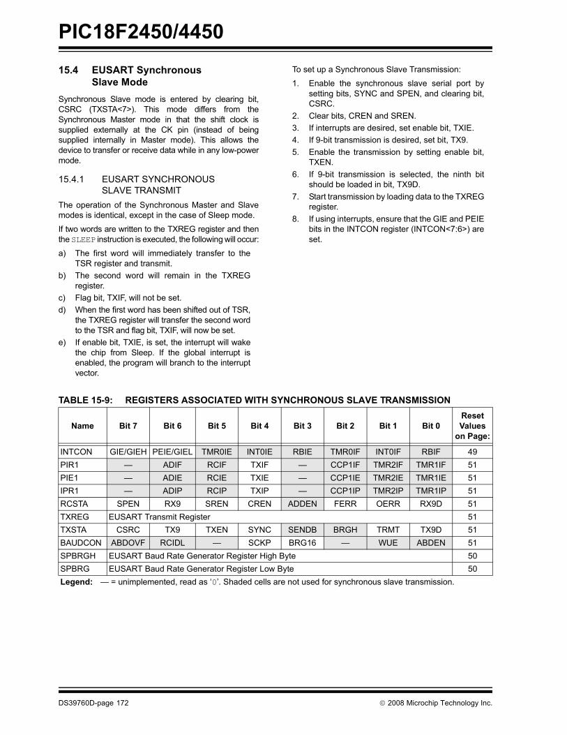
PIC18F2450/4450
DS39760D-page 172 © 2008 Microchip Technology Inc.
15.4 EUSART Synchronous Slave Mode
Synchronous Slave mode is entered by clearing bit,CSRC (TXSTA<7>). This mode differs from theSynchronous Master mode in that the shift clock issupplied externally at the CK pin (instead of beingsupplied internally in Master mode). This allows thedevice to transfer or receive data while in any low-powermode.
15.4.1 EUSART SYNCHRONOUS SLAVE TRANSMIT
The operation of the Synchronous Master and Slavemodes is identical, except in the case of Sleep mode.
If two words are written to the TXREG register and thenthe SLEEP instruction is executed, the following will occur:
a) The first word will immediately transfer to theTSR register and transmit.
b) The second word will remain in the TXREGregister.
c) Flag bit, TXIF, will not be set. d) When the first word has been shifted out of TSR,
the TXREG register will transfer the second wordto the TSR and flag bit, TXIF, will now be set.
e) If enable bit, TXIE, is set, the interrupt will wakethe chip from Sleep. If the global interrupt isenabled, the program will branch to the interruptvector.
To set up a Synchronous Slave Transmission:
1. Enable the synchronous slave serial port bysetting bits, SYNC and SPEN, and clearing bit,CSRC.
2. Clear bits, CREN and SREN.3. If interrupts are desired, set enable bit, TXIE.4. If 9-bit transmission is desired, set bit, TX9.5. Enable the transmission by setting enable bit,
TXEN.6. If 9-bit transmission is selected, the ninth bit
should be loaded in bit, TX9D.7. Start transmission by loading data to the TXREG
register.8. If using interrupts, ensure that the GIE and PEIE
bits in the INTCON register (INTCON<7:6>) areset.
TABLE 15-9: REGISTERS ASSOCIATED WITH SYNCHRONOUS SLAVE TRANSMISSION
Name Bit 7 Bit 6 Bit 5 Bit 4 Bit 3 Bit 2 Bit 1 Bit 0Reset Values
on Page:
INTCON GIE/GIEH PEIE/GIEL TMR0IE INT0IE RBIE TMR0IF INT0IF RBIF 49PIR1 � ADIF RCIF TXIF � CCP1IF TMR2IF TMR1IF 51PIE1 � ADIE RCIE TXIE � CCP1IE TMR2IE TMR1IE 51IPR1 � ADIP RCIP TXIP � CCP1IP TMR2IP TMR1IP 51RCSTA SPEN RX9 SREN CREN ADDEN FERR OERR RX9D 51TXREG EUSART Transmit Register 51TXSTA CSRC TX9 TXEN SYNC SENDB BRGH TRMT TX9D 51BAUDCON ABDOVF RCIDL � SCKP BRG16 � WUE ABDEN 51SPBRGH EUSART Baud Rate Generator Register High Byte 50SPBRG EUSART Baud Rate Generator Register Low Byte 50Legend: � = unimplemented, read as �0�. Shaded cells are not used for synchronous slave transmission.

PIC18F2450/4450
© 2008 Microchip Technology Inc. DS39760D-page 173
15.4.2 EUSART SYNCHRONOUS SLAVE RECEPTION
The operation of the Synchronous Master and Slavemodes is identical, except in the case of Sleep or anyIdle mode and bit, SREN, which is a �don�t care� inSlave mode.
If receive is enabled by setting the CREN bit prior toentering Sleep or any Idle mode, then a word may bereceived while in this low-power mode. Once the wordis received, the RSR register will transfer the data to theRCREG register. If the RCIE enable bit is set, theinterrupt generated will wake the chip from the low-power mode. If the global interrupt is enabled, theprogram will branch to the interrupt vector.
To set up a Synchronous Slave Reception:
1. Enable the synchronous master serial port bysetting bits, SYNC and SPEN, and clearing bit,CSRC.
2. If interrupts are desired, set enable bit, RCIE.3. If 9-bit reception is desired, set bit, RX9.4. To enable reception, set enable bit, CREN.5. Flag bit RCIF will be set when reception is
complete. An interrupt will be generated ifenable bit, RCIE, was set.
6. Read the RCSTA register to get the ninth bit (ifenabled) and determine if any error occurredduring reception.
7. Read the 8-bit received data by reading theRCREG register.
8. If any error occurred, clear the error by clearingbit, CREN.
9. If using interrupts, ensure that the GIE and PEIEbits in the INTCON register (INTCON<7:6>) areset.
TABLE 15-10: REGISTERS ASSOCIATED WITH SYNCHRONOUS SLAVE RECEPTION
Name Bit 7 Bit 6 Bit 5 Bit 4 Bit 3 Bit 2 Bit 1 Bit 0Reset Values
on Page:
INTCON GIE/GIEH PEIE/GIEL TMR0IE INT0IE RBIE TMR0IF INT0IF RBIF 49PIR1 � ADIF RCIF TXIF � CCP1IF TMR2IF TMR1IF 51PIE1 � ADIE RCIE TXIE � CCP1IE TMR2IE TMR1IE 51IPR1 � ADIP RCIP TXIP � CCP1IP TMR2IP TMR1IP 51RCSTA SPEN RX9 SREN CREN ADDEN FERR OERR RX9D 51RCREG EUSART Receive Register 50TXSTA CSRC TX9 TXEN SYNC SENDB BRGH TRMT TX9D 51BAUDCON ABDOVF RCIDL � SCKP BRG16 � WUE ABDEN 51SPBRGH EUSART Baud Rate Generator Register High Byte 50SPBRG EUSART Baud Rate Generator Register Low Byte 50Legend: � = unimplemented, read as �0�. Shaded cells are not used for synchronous slave reception.

PIC18F2450/4450
DS39760D-page 174 © 2008 Microchip Technology Inc.
NOTES:

PIC18F2450/4450
© 2008 Microchip Technology Inc. DS39760D-page 175
16.0 10-BIT ANALOG-TO-DIGITAL CONVERTER (A/D) MODULE
The Analog-to-Digital (A/D) Converter module has10 inputs for the 28-pin devices and 13 for the 40/44-pindevices. This module allows conversion of an analoginput signal to a corresponding 10-bit digital number.
The module has five registers:
� A/D Result High Register (ADRESH)� A/D Result Low Register (ADRESL)� A/D Control Register 0 (ADCON0)� A/D Control Register 1 (ADCON1)� A/D Control Register 2 (ADCON2)
The ADCON0 register, shown in Register 16-1,controls the operation of the A/D module. TheADCON1 register, shown in Register 16-2, configuresthe functions of the port pins. The ADCON2 register,shown in Register 16-3, configures the A/D clocksource, programmed acquisition time and justification.
REGISTER 16-1: ADCON0: A/D CONTROL REGISTER 0
U0 U-0 R/W-0 R/W-0 R/W-0 R/W-0 R/W-0 R/W-0
� � CHS3 CHS2 CHS1 CHS0 GO/DONE ADONbit 7 bit 0
Legend:R = Readable bit W = Writable bit U = Unimplemented bit, read as �0�-n = Value at POR �1� = Bit is set �0� = Bit is cleared x = Bit is unknown
bit 7-6 Unimplemented: Read as �0�bit 5-2 CHS3:CHS0: Analog Channel Select bits
0000 = Channel 0 (AN0)0001 = Channel 1 (AN1)0010 = Channel 2 (AN2)0011 = Channel 3 (AN3)0100 = Channel 4 (AN4)0101 = Channel 5 (AN5)(1,2) 0110 = Channel 6 (AN6)(1,2) 0111 = Channel 7 (AN7)(1,2)
1000 = Channel 8 (AN8)1001 = Channel 9 (AN9)1010 = Channel 10 (AN10)1011 = Channel 11 (AN11)1100 = Channel 12 (AN121101 = Unimplemented(2)
1110 = Unimplemented(2)
1111 = Unimplemented(2)
bit 1 GO/DONE: A/D Conversion Status bitWhen ADON = 1: 1 = A/D conversion in progress0 = A/D Idle
bit 0 ADON: A/D On bit1 = A/D Converter module is enabled 0 = A/D Converter module is disabled
Note 1: These channels are not implemented on 28-pin devices.2: Performing a conversion on unimplemented channels will return a floating input measurement.

PIC18F2450/4450
DS39760D-page 176 © 2008 Microchip Technology Inc.
REGISTER 16-2: ADCON1: A/D CONTROL REGISTER 1
U-0 U-0 R/W-0 R/W-0 R/W-0(1) R/W(1) R/W(1) R/W(1)
� � VCFG1 VCFG0 PCFG3 PCFG2 PCFG1 PCFG0bit 7 bit 0
Legend:R = Readable bit W = Writable bit U = Unimplemented bit, read as �0�-n = Value at POR �1� = Bit is set �0� = Bit is cleared x = Bit is unknown
bit 7-6 Unimplemented: Read as �0�bit 5 VCFG1: Voltage Reference Configuration bit (VREF- source)
1 = VREF- (AN2)0 = VSS
bit 4 VCFG0: Voltage Reference Configuration bit (VREF+ source)1 = VREF+ (AN3)0 = VDD
bit 3-0 PCFG3:PCFG0: A/D Port Configuration Control bits:
Note 1: The POR value of the PCFG bits depends on the value of the PBADEN Configuration bit. When PBADEN = 1, PCFG<3:0> = 0000; when PBADEN = 0, PCFG<3:0> = 0111.
2: AN5 through AN7 are available only on 40/44-pin devices.
A = Analog input D = Digital I/O
PCFG3:PCFG0 A
N12
AN
11
AN
10
AN
9
AN
8
AN
7(2)
AN
6(2)
AN
5(2)
AN
4
AN
3
AN
2
AN
1
AN
0
0000(1) A A A A A A A A A A A A A
0001 A A A A A A A A A A A A A0010 A A A A A A A A A A A A A0011 D A A A A A A A A A A A A0100 D D A A A A A A A A A A A0101 D D D A A A A A A A A A A0110 D D D D A A A A A A A A A
0111(1) D D D D D A A A A A A A A
1000 D D D D D D A A A A A A A1001 D D D D D D D A A A A A A1010 D D D D D D D D A A A A A1011 D D D D D D D D D A A A A1100 D D D D D D D D D D A A A1101 D D D D D D D D D D D A A1110 D D D D D D D D D D D D A1111 D D D D D D D D D D D D D

PIC18F2450/4450
© 2008 Microchip Technology Inc. DS39760D-page 177
REGISTER 16-3: ADCON2: A/D CONTROL REGISTER 2
R/W-0 U-0 R/W-0 R/W-0 R/W-0 R/W-0 R/W-0 R/W-0ADFM � ACQT2 ACQT1 ACQT0 ADCS2 ADCS1 ADCS0
bit 7 bit 0
Legend:R = Readable bit W = Writable bit U = Unimplemented bit, read as �0�-n = Value at POR �1� = Bit is set �0� = Bit is cleared x = Bit is unknown
bit 7 ADFM: A/D Result Format Select bit1 = Right justified 0 = Left justified
bit 6 Unimplemented: Read as �0�bit 5-3 ACQT2:ACQT0: A/D Acquisition Time Select bits
111 = 20 TAD110 = 16 TAD101 = 12 TAD100 = 8 TAD011 = 6 TAD010 = 4 TAD001 = 2 TAD000 = 0 TAD(1)
bit 2-0 ADCS2:ADCS0: A/D Conversion Clock Select bits111 = FRC (clock derived from A/D RC oscillator)(1) 110 = FOSC/64 101 = FOSC/16 100 = FOSC/4 011 = FRC (clock derived from A/D RC oscillator)(1) 010 = FOSC/32 001 = FOSC/8 000 = FOSC/2
Note 1: If the A/D FRC clock source is selected, a delay of one TCY (instruction cycle) is added before the A/D clock starts. This allows the SLEEP instruction to be executed before starting a conversion.
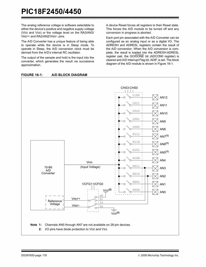
PIC18F2450/4450
DS39760D-page 178 © 2008 Microchip Technology Inc.
The analog reference voltage is software selectable toeither the device�s positive and negative supply voltage(VDD and VSS) or the voltage level on the RA3/AN3/VREF+ and RA2/AN2/VREF- pins.
The A/D Converter has a unique feature of being ableto operate while the device is in Sleep mode. Tooperate in Sleep, the A/D conversion clock must bederived from the A/D�s internal RC oscillator.
The output of the sample and hold is the input into theconverter, which generates the result via successiveapproximation.
A device Reset forces all registers to their Reset state.This forces the A/D module to be turned off and anyconversion in progress is aborted.
Each port pin associated with the A/D Converter can beconfigured as an analog input or as a digital I/O. TheADRESH and ADRESL registers contain the result ofthe A/D conversion. When the A/D conversion is com-plete, the result is loaded into the ADRESH:ADRESLregister pair, the GO/DONE bit (ADCON0 register) iscleared and A/D Interrupt Flag bit, ADIF, is set. The blockdiagram of the A/D module is shown in Figure 16-1.
FIGURE 16-1: A/D BLOCK DIAGRAM
(Input Voltage)VAIN
VREF+Reference
Voltage
VDD(2)
VCFG1:VCFG0
CHS3:CHS0
AN7(1)
AN6(1)
AN5(1)
AN4
AN3
AN2
AN1
AN0
0111
0110
0101
0100
0011
0010
0001
0000
10-BitA/D
VREF-
VSS(2)
Converter
AN12
AN11
AN10
AN9
AN8
1100
1011
1010
1001
1000
Note 1: Channels AN5 through AN7 are not available on 28-pin devices.2: I/O pins have diode protection to VDD and VSS.
0X1XX1X0
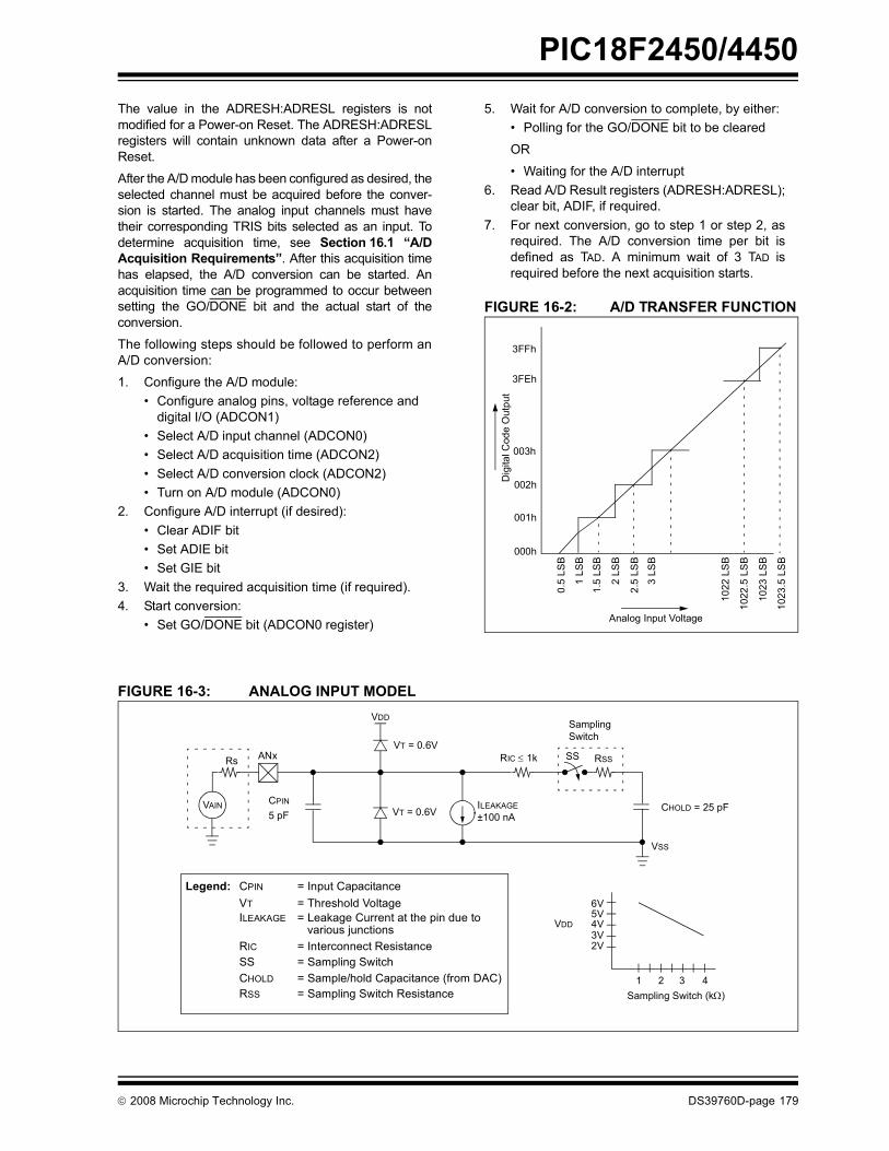
PIC18F2450/4450
© 2008 Microchip Technology Inc. DS39760D-page 179
The value in the ADRESH:ADRESL registers is notmodified for a Power-on Reset. The ADRESH:ADRESLregisters will contain unknown data after a Power-onReset.
After the A/D module has been configured as desired, theselected channel must be acquired before the conver-sion is started. The analog input channels must havetheir corresponding TRIS bits selected as an input. Todetermine acquisition time, see Section 16.1 �A/DAcquisition Requirements�. After this acquisition timehas elapsed, the A/D conversion can be started. Anacquisition time can be programmed to occur betweensetting the GO/DONE bit and the actual start of theconversion.
The following steps should be followed to perform anA/D conversion:
1. Configure the A/D module:� Configure analog pins, voltage reference and
digital I/O (ADCON1)� Select A/D input channel (ADCON0)� Select A/D acquisition time (ADCON2)� Select A/D conversion clock (ADCON2)� Turn on A/D module (ADCON0)
2. Configure A/D interrupt (if desired):� Clear ADIF bit � Set ADIE bit � Set GIE bit
3. Wait the required acquisition time (if required).4. Start conversion:
� Set GO/DONE bit (ADCON0 register)
5. Wait for A/D conversion to complete, by either:� Polling for the GO/DONE bit to be cleared
OR
� Waiting for the A/D interrupt6. Read A/D Result registers (ADRESH:ADRESL);
clear bit, ADIF, if required.7. For next conversion, go to step 1 or step 2, as
required. The A/D conversion time per bit isdefined as TAD. A minimum wait of 3 TAD isrequired before the next acquisition starts.
FIGURE 16-2: A/D TRANSFER FUNCTION
FIGURE 16-3: ANALOG INPUT MODEL
Dig
ital C
ode
Out
put
3FEh
003h
002h
001h
000h0.
5 LS
B
1 LS
B
1.5
LSB
2 LS
B
2.5
LSB
1022
LS
B
1022
.5 L
SB
3 LS
B
Analog Input Voltage
3FFh
1023
LS
B
1023
.5 L
SB
VAIN CPIN
Rs ANx
5 pF
VT = 0.6V
VT = 0.6VILEAKAGE
RIC ≤ 1k
SamplingSwitch
SS RSS
CHOLD = 25 pF
VSS
VDD
±100 nA
Legend: CPIN
VTILEAKAGE
RIC
SSCHOLD
= Input Capacitance= Threshold Voltage= Leakage Current at the pin due to
= Interconnect Resistance= Sampling Switch= Sample/hold Capacitance (from DAC)
various junctions
= Sampling Switch ResistanceRSS
VDD
6V
Sampling Switch
5V4V3V2V
1 2 3 4(kΩ)

PIC18F2450/4450
DS39760D-page 180 © 2008 Microchip Technology Inc.
16.1 A/D Acquisition RequirementsFor the A/D Converter to meet its specified accuracy,the charge holding capacitor (CHOLD) must be allowedto fully charge to the input channel voltage level. Theanalog input model is shown in Figure 16-3. Thesource impedance (RS) and the internal samplingswitch (RSS) impedance directly affect the timerequired to charge the capacitor CHOLD. The samplingswitch (RSS) impedance varies over the device voltage(VDD). The source impedance affects the offset voltageat the analog input (due to pin leakage current). Themaximum recommended impedance for analogsources is 2.5 kΩ. After the analog input channel isselected (changed), the channel must be sampled forat least the minimum acquisition time before starting aconversion.
To calculate the minimum acquisition time,Equation 16-1 may be used. This equation assumesthat 1/2 LSb error is used (1024 steps for the A/D). The1/2 LSb error is the maximum error allowed for the A/Dto meet its specified resolution.
Example 16-3 shows the calculation of the minimumrequired acquisition time TACQ. This calculation isbased on the following application systemassumptions:
CHOLD = 25 pF Rs = 2.5 kΩ Conversion Error ≤ 1/2 LSb VDD = 5V → RSS = 2 kΩ Temperature = 85°C (system max.)
EQUATION 16-1: ACQUISITION TIME
EQUATION 16-2: A/D MINIMUM CHARGING TIME
EQUATION 16-3: CALCULATING THE MINIMUM REQUIRED ACQUISITION TIME
Note: When the conversion is started, theholding capacitor is disconnected from theinput pin.
TACQ = Amplifier Settling Time + Holding Capacitor Charging Time + Temperature Coefficient
= TAMP + TC + TCOFF
VHOLD = (VREF � (VREF/2048)) � (1 � e(-TC/CHOLD(RIC + RSS + RS))) or TC = -(CHOLD)(RIC + RSS + RS) ln(1/2048)
TACQ = TAMP + TC + TCOFF
TAMP = 0.2 μs
TCOFF = (Temp � 25°C)(0.02 μs/°C)(85°C � 25°C)(0.02 μs/°C)1.2 μs
Temperature coefficient is only required for temperatures > 25°C. Below 25°C, TCOFF = 0 ms.
TC = -(CHOLD)(RIC + RSS + RS) ln(1/2047) μs-(25 pF) (1 kΩ + 2 kΩ + 2.5 kΩ) ln(0.0004883) μs 1.05 μs
TACQ = 0.2 μs + 1 μs + 1.2 μs2.4 μs

PIC18F2450/4450
© 2008 Microchip Technology Inc. DS39760D-page 181
16.2 Selecting and Configuring Acquisition Time
The ADCON2 register allows the user to select anacquisition time that occurs each time the GO/DONEbit is set. It also gives users the option to use anautomatically determined acquisition time.
Acquisition time may be set with the ACQT2:ACQT0 bits(ADCON2<5:3>) which provide a range of 2 to 20 TAD.When the GO/DONE bit is set, the A/D modulecontinues to sample the input for the selected acquisitiontime, then automatically begins a conversion. Since theacquisition time is programmed, there may be no needto wait for an acquisition time between selecting achannel and setting the GO/DONE bit.
Manual acquisition is selected whenACQT2:ACQT0 = 000. When the GO/DONE bit is set,sampling is stopped and a conversion begins. The useris responsible for ensuring the required acquisition timehas passed between selecting the desired inputchannel and setting the GO/DONE bit. This option isalso the default Reset state of the ACQT2:ACQT0 bitsand is compatible with devices that do not offerprogrammable acquisition times.
In either case, when the conversion is completed, theGO/DONE bit is cleared, the ADIF flag is set and theA/D begins sampling the currently selected channelagain. If an acquisition time is programmed, there isnothing to indicate if the acquisition time has ended orif the conversion has begun.
16.3 Selecting the A/D Conversion Clock
The A/D conversion time per bit is defined as TAD. TheA/D conversion requires 11 TAD per 10-bit conversion.The source of the A/D conversion clock is softwareselectable. There are seven possible options for TAD:
� 2 TOSC
� 4 TOSC
� 8 TOSC
� 16 TOSC
� 32 TOSC � 64 TOSC
� Internal RC Oscillator
For correct A/D conversions, the A/D conversion clock(TAD) must be as short as possible but greater than theminimum TAD (see parameter 130 in Table 21-18 formore information).
Table 16-1 shows the resultant TAD times derived fromthe device operating frequencies and the A/D clocksource selected.
TABLE 16-1: TAD vs. DEVICE OPERATING FREQUENCIES AD Clock Source (TAD) Maximum Device Frequency
Operation ADCS2:ADCS0 PIC18FX450 PIC18LFX450(4)
2 TOSC 000 2.86 MHz 1.43 MHz4 TOSC 100 5.71 MHz 2.86 MHz8 TOSC 001 11.43 MHz 5.72 MHz
16 TOSC 101 22.86 MHz 11.43 MHz32 TOSC 010 45.71 MHz 22.86 MHz64 TOSC 110 48.0 MHz 45.71 MHz
RC(3) x11 1.00 MHz(1) 1.00 MHz(2)
Note 1: The RC source has a typical TAD time of 1.2 μs.2: The RC source has a typical TAD time of 2.5 μs.3: For device frequencies above 1 MHz, the device must be in Sleep for the entire conversion or the A/D
accuracy may be out of specification.4: Low-power devices only.
PIC18F2450/4450
DS39760D-page 182 © 2008 Microchip Technology Inc.
16.4 Operation in Power-Managed Modes
The selection of the automatic acquisition time andA/D conversion clock is determined in part by the clocksource and frequency while in a power-managedmode.
If the A/D is expected to operate while the device is ina power-managed mode, the ACQT2:ACQT0 andADCS2:ADCS0 bits in ADCON2 should be updated inaccordance with the clock source to be used in thatmode. After entering the mode, an A/D acquisition orconversion may be started. Once started, the deviceshould continue to be clocked by the same clocksource until the conversion has been completed.
If desired, the device may be placed into thecorresponding Idle mode during the conversion. If thedevice clock frequency is less than 1 MHz, the A/D RCclock source should be selected.
Operation in the Sleep mode requires the A/D FRCclock to be selected. If bits ACQT2:ACQT0 are set to�000� and a conversion is started, the conversion will bedelayed one instruction cycle to allow execution of theSLEEP instruction and entry to Sleep mode. The IDLENbit (OSCCON<7>) must have already been clearedprior to starting the conversion.
16.5 Configuring Analog Port PinsThe ADCON1, TRISA, TRISB and TRISE registers allconfigure the A/D port pins. The port pins needed asanalog inputs must have their corresponding TRIS bitsset (input). If the TRIS bit is cleared (output), the digitaloutput level (VOH or VOL) will be converted.
The A/D operation is independent of the state of theCHS3:CHS0 bits and the TRIS bits.
Note 1: When reading the PORT register, all pinsconfigured as analog input channels willread as cleared (a low level). Pins config-ured as digital inputs will convert as ana-log inputs. Analog levels on a digitallyconfigured input will be accuratelyconverted.
2: Analog levels on any pin defined as adigital input may cause the digital inputbuffer to consume current out of thedevice�s specification limits.
3: The PBADEN bit in ConfigurationRegister 3H configures PORTB pins toreset as analog or digital pins by control-ling how the PCFG0 bits in ADCON1 arereset.
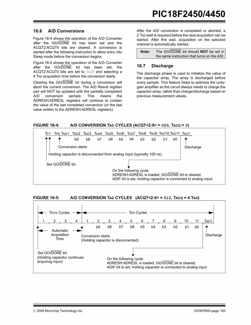
PIC18F2450/4450
© 2008 Microchip Technology Inc. DS39760D-page 183
16.6 A/D Conversions Figure 16-4 shows the operation of the A/D Converterafter the GO/DONE bit has been set and theACQT2:ACQT0 bits are cleared. A conversion isstarted after the following instruction to allow entry intoSleep mode before the conversion begins.
Figure 16-5 shows the operation of the A/D Converterafter the GO/DONE bit has been set, theACQT2:ACQT0 bits are set to �010� and selecting a4 TAD acquisition time before the conversion starts.
Clearing the GO/DONE bit during a conversion willabort the current conversion. The A/D Result registerpair will NOT be updated with the partially completedA/D conversion sample. This means theADRESH:ADRESL registers will continue to containthe value of the last completed conversion (or the lastvalue written to the ADRESH:ADRESL registers).
After the A/D conversion is completed or aborted, a2 TAD wait is required before the next acquisition can bestarted. After this wait, acquisition on the selectedchannel is automatically started.
16.7 DischargeThe discharge phase is used to initialize the value ofthe capacitor array. The array is discharged beforeevery sample. This feature helps to optimize the unity-gain amplifier as the circuit always needs to charge thecapacitor array, rather than charge/discharge based onprevious measurement values.
FIGURE 16-4: A/D CONVERSION TAD CYCLES (ACQT<2:0> = 000, TACQ = 0)
FIGURE 16-5: A/D CONVERSION TAD CYCLES (ACQT<2:0> = 010, TACQ = 4 TAD)
Note: The GO/DONE bit should NOT be set inthe same instruction that turns on the A/D.
TAD1 TAD2 TAD3 TAD4 TAD5 TAD6 TAD7 TAD8 TAD11
Set GO/DONE bit
Holding capacitor is disconnected from analog input (typically 100 ns)
TAD9 TAD10TCY - TAD
ADRESH:ADRESL is loaded, GO/DONE bit is cleared, ADIF bit is set, holding capacitor is connected to analog input.
Conversion starts
b0b9 b6 b5 b4 b3 b2 b1b8 b7
On the following cycle:
TAD1
Discharge
1 2 3 4 5 6 7 8 11
Set GO/DONE bit
(Holding capacitor is disconnected)
9 10
Conversion starts
1 2 3 4
(Holding capacitor continuesacquiring input)
TACQ Cycles TAD Cycles
AutomaticAcquisition
Time
b0b9 b6 b5 b4 b3 b2 b1b8 b7
ADRESH:ADRESL is loaded, GO/DONE bit is cleared, ADIF bit is set, holding capacitor is connected to analog input.
On the following cycle:
TAD1
Discharge
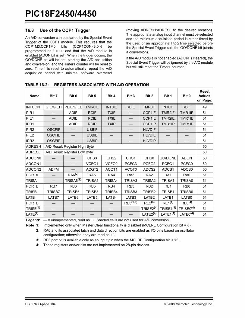
PIC18F2450/4450
DS39760D-page 184 © 2008 Microchip Technology Inc.
16.8 Use of the CCP1 TriggerAn A/D conversion can be started by the Special EventTrigger of the CCP1 module. This requires that theCCP1M3:CCP1M0 bits (CCP1CON<3:0>) beprogrammed as �1011� and that the A/D module isenabled (ADON bit is set). When the trigger occurs, theGO/DONE bit will be set, starting the A/D acquisitionand conversion, and the Timer1 counter will be reset tozero. Timer1 is reset to automatically repeat the A/Dacquisition period with minimal software overhead
(moving ADRESH:ADRESL to the desired location).The appropriate analog input channel must be selectedand the minimum acquisition period is either timed bythe user, or an appropriate TACQ time selected beforethe Special Event Trigger sets the GO/DONE bit (startsa conversion).
If the A/D module is not enabled (ADON is cleared), theSpecial Event Trigger will be ignored by the A/D modulebut will still reset the Timer1 counter.
TABLE 16-2: REGISTERS ASSOCIATED WITH A/D OPERATION
Name Bit 7 Bit 6 Bit 5 Bit 4 Bit 3 Bit 2 Bit 1 Bit 0Reset Values
on Page:
INTCON GIE/GIEH PEIE/GIEL TMR0IE INT0IE RBIE TMR0IF INT0IF RBIF 49PIR1 � ADIF RCIF TXIF � CCP1IF TMR2IF TMR1IF 51PIE1 � ADIE RCIE TXIE � CCP1IE TMR2IE TMR1IE 51IPR1 � ADIP RCIP TXIP � CCP1IP TMR2IP TMR1IP 51PIR2 OSCFIF � USBIF � � HLVDIF � � 51PIE2 OSCFIE � USBIE � � HLVDIE � � 51IPR2 OSCFIP � USBIP � � HLVDIP � � 51ADRESH A/D Result Register High Byte 50ADRESL A/D Result Register Low Byte 50
ADCON0 � � CHS3 CHS2 CHS1 CHS0 GO/DONE ADON 50ADCON1 � � VCFG1 VCFG0 PCFG3 PCFG2 PCFG1 PCFG0 50ADCON2 ADFM � ACQT2 ACQT1 ACQT0 ADCS2 ADCS1 ADCS0 50PORTA � RA6(2) RA5 RA4 RA3 RA2 RA1 RA0 51TRISA � TRISA6(2) TRISA5 TRISA4 TRISA3 TRISA2 TRISA1 TRISA0 51PORTB RB7 RB6 RB5 RB4 RB3 RB2 RB1 RB0 51TRISB TRISB7 TRISB6 TRISB5 TRISB4 TRISB3 TRISB2 TRISB1 TRISB0 51LATB LATB7 LATB6 LATB5 LATB4 LATB3 LATB2 LATB1 LATB0 51PORTE � � � � RE3(1,3) RE2(4) RE1(4) RE0(4) 51TRISE(4) � � � � � TRISE2(4) TRISE1(4) TRISE0(4) 51LATE(4) � � � � � LATE2(4) LATE1(4) LATE0(4) 51Legend: � = unimplemented, read as �0�. Shaded cells are not used for A/D conversion.Note 1: Implemented only when Master Clear functionality is disabled (MCLRE Configuration bit = 0).
2: RA6 and its associated latch and data direction bits are enabled as I/O pins based on oscillator configuration; otherwise, they are read as �0�.
3: RE3 port bit is available only as an input pin when the MCLRE Configuration bit is �0�.4: These registers and/or bits are not implemented on 28-pin devices.
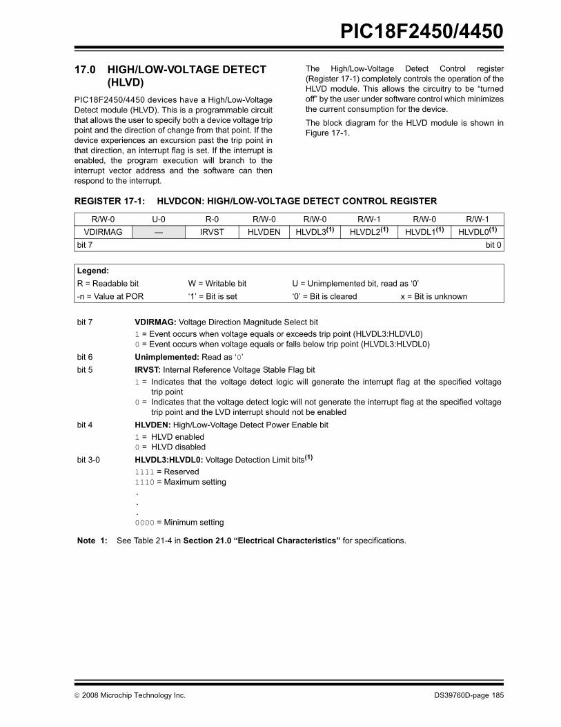
PIC18F2450/4450
© 2008 Microchip Technology Inc. DS39760D-page 185
17.0 HIGH/LOW-VOLTAGE DETECT (HLVD)
PIC18F2450/4450 devices have a High/Low-VoltageDetect module (HLVD). This is a programmable circuitthat allows the user to specify both a device voltage trippoint and the direction of change from that point. If thedevice experiences an excursion past the trip point inthat direction, an interrupt flag is set. If the interrupt isenabled, the program execution will branch to theinterrupt vector address and the software can thenrespond to the interrupt.
The High/Low-Voltage Detect Control register(Register 17-1) completely controls the operation of theHLVD module. This allows the circuitry to be �turnedoff� by the user under software control which minimizesthe current consumption for the device.
The block diagram for the HLVD module is shown inFigure 17-1.
REGISTER 17-1: HLVDCON: HIGH/LOW-VOLTAGE DETECT CONTROL REGISTER
R/W-0 U-0 R-0 R/W-0 R/W-0 R/W-1 R/W-0 R/W-1VDIRMAG � IRVST HLVDEN HLVDL3(1) HLVDL2(1) HLVDL1(1) HLVDL0(1)
bit 7 bit 0
Legend:R = Readable bit W = Writable bit U = Unimplemented bit, read as �0�-n = Value at POR �1� = Bit is set �0� = Bit is cleared x = Bit is unknown
bit 7 VDIRMAG: Voltage Direction Magnitude Select bit1 = Event occurs when voltage equals or exceeds trip point (HLVDL3:HLDVL0)0 = Event occurs when voltage equals or falls below trip point (HLVDL3:HLVDL0)
bit 6 Unimplemented: Read as �0�bit 5 IRVST: Internal Reference Voltage Stable Flag bit
1 = Indicates that the voltage detect logic will generate the interrupt flag at the specified voltagetrip point
0 = Indicates that the voltage detect logic will not generate the interrupt flag at the specified voltagetrip point and the LVD interrupt should not be enabled
bit 4 HLVDEN: High/Low-Voltage Detect Power Enable bit1 = HLVD enabled0 = HLVD disabled
bit 3-0 HLVDL3:HLVDL0: Voltage Detection Limit bits(1)
1111 = Reserved 1110 = Maximum setting ...0000 = Minimum setting
Note 1: See Table 21-4 in Section 21.0 �Electrical Characteristics� for specifications.

PIC18F2450/4450
DS39760D-page 186 © 2008 Microchip Technology Inc.
The module is enabled by setting the HLVDEN bit.Each time that the HLVD module is enabled, thecircuitry requires some time to stabilize. The IRVST bitis a read-only bit and is used to indicate when the circuitis stable. The module can only generate an interruptafter the circuit is stable and IRVST is set.
The VDIRMAG bit determines the overall operation ofthe module. When VDIRMAG is cleared, the modulemonitors for drops in VDD below a predetermined setpoint. When the bit is set, the module monitors for risesin VDD above the set point.
17.1 OperationWhen the HLVD module is enabled, a comparator usesan internally generated reference voltage as the setpoint. The set point is compared with the trip point,where each node in the resistor divider represents atrip point voltage. The �trip point� voltage is the voltagelevel at which the device detects a high or low-voltage
event, depending on the configuration of the module.When the supply voltage is equal to the trip point, thevoltage tapped off of the resistor array is equal to theinternal reference voltage generated by the voltagereference module. The comparator then generates aninterrupt signal by setting the HLVDIF bit.
The trip point voltage is software programmable to anyone of 16 values. The trip point is selected byprogramming the HLVDL3:HLVDL0 bits(HLVDCON<3:0>).
The HLVD module has an additional feature that allowsthe user to supply the trip voltage to the module from anexternal source. This mode is enabled when bits,HLVDL3:HLVDL0, are set to �1111�. In this state, thecomparator input is multiplexed from the external inputpin, HLVDIN. This gives users flexibility because itallows them to configure the High/Low-Voltage Detectinterrupt to occur at any voltage in the valid operatingrange.
FIGURE 17-1: HLVD MODULE BLOCK DIAGRAM (WITH EXTERNAL INPUT)
Set
VDD
16-to
-1 M
UX
HLVDEN
HLVDCONHLVDL3:HLVDL0Register
HLVDIN
VDD
Externally GeneratedTrip Point
HLVDIF
HLVDEN
BOREN
Internal VoltageReference
VDIRMAG
1.2V Typical
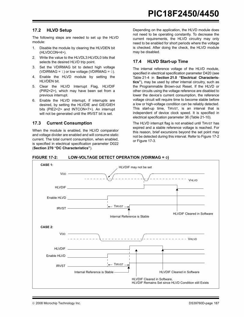
PIC18F2450/4450
© 2008 Microchip Technology Inc. DS39760D-page 187
17.2 HLVD SetupThe following steps are needed to set up the HLVDmodule:
1. Disable the module by clearing the HLVDEN bit(HLVDCON<4>).
2. Write the value to the HLVDL3:HLVDL0 bits thatselects the desired HLVD trip point.
3. Set the VDIRMAG bit to detect high voltage(VDIRMAG = 1) or low voltage (VDIRMAG = 0).
4. Enable the HLVD module by setting theHLVDEN bit.
5. Clear the HLVD Interrupt Flag, HLVDIF(PIR2<2>), which may have been set from aprevious interrupt.
6. Enable the HLVD interrupt, if interrupts aredesired, by setting the HLVDIE and GIE/GIEHbits (PIE2<2> and INTCON<7>). An interruptwill not be generated until the IRVST bit is set.
17.3 Current ConsumptionWhen the module is enabled, the HLVD comparatorand voltage divider are enabled and will consume staticcurrent. The total current consumption, when enabled,is specified in electrical specification parameter D022(Section 270 �DC Characteristics�).
Depending on the application, the HLVD module doesnot need to be operating constantly. To decrease thecurrent requirements, the HLVD circuitry may onlyneed to be enabled for short periods where the voltageis checked. After doing the check, the HLVD modulemay be disabled.
17.4 HLVD Start-up TimeThe internal reference voltage of the HLVD module,specified in electrical specification parameter D420 (seeTable 21-4 in Section 21.0 �Electrical Characteris-tics�), may be used by other internal circuitry, such asthe Programmable Brown-out Reset. If the HLVD orother circuits using the voltage reference are disabled tolower the device�s current consumption, the referencevoltage circuit will require time to become stable beforea low or high-voltage condition can be reliably detected.This start-up time, TIRVST, is an interval that isindependent of device clock speed. It is specified inelectrical specification parameter 36 (Table 21-10).
The HLVD interrupt flag is not enabled until TIRVST hasexpired and a stable reference voltage is reached. Forthis reason, brief excursions beyond the set point maynot be detected during this interval. Refer to Figure 17-2or Figure 17-3.
FIGURE 17-2: LOW-VOLTAGE DETECT OPERATION (VDIRMAG = 0)
VHLVD
VDD
HLVDIF
VHLVD
VDD
Enable HLVD
TIRVST
HLVDIF may not be set
Enable HLVD
HLVDIF
HLVDIF Cleared in Software
HLVDIF Cleared in Software
HLVDIF Cleared in Software,
CASE 1:
CASE 2:
HLVDIF Remains Set since HLVD Condition still Exists
TIRVST
Internal Reference is Stable
Internal Reference is Stable
IRVST
IRVST
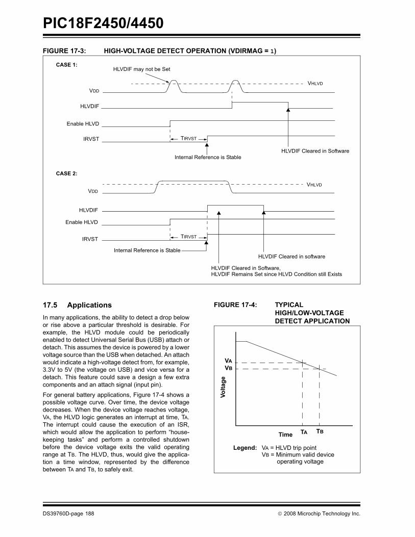
PIC18F2450/4450
DS39760D-page 188 © 2008 Microchip Technology Inc.
FIGURE 17-3: HIGH-VOLTAGE DETECT OPERATION (VDIRMAG = 1)
17.5 ApplicationsIn many applications, the ability to detect a drop belowor rise above a particular threshold is desirable. Forexample, the HLVD module could be periodicallyenabled to detect Universal Serial Bus (USB) attach ordetach. This assumes the device is powered by a lowervoltage source than the USB when detached. An attachwould indicate a high-voltage detect from, for example,3.3V to 5V (the voltage on USB) and vice versa for adetach. This feature could save a design a few extracomponents and an attach signal (input pin).
For general battery applications, Figure 17-4 shows apossible voltage curve. Over time, the device voltagedecreases. When the device voltage reaches voltage,VA, the HLVD logic generates an interrupt at time, TA.The interrupt could cause the execution of an ISR,which would allow the application to perform �house-keeping tasks� and perform a controlled shutdownbefore the device voltage exits the valid operatingrange at TB. The HLVD, thus, would give the applica-tion a time window, represented by the differencebetween TA and TB, to safely exit.
FIGURE 17-4: TYPICAL HIGH/LOW-VOLTAGE DETECT APPLICATION
VHLVD
VDD
HLVDIF
VHLVDVDD
Enable HLVD
TIRVST
HLVDIF may not be Set
Enable HLVD
HLVDIF
HLVDIF Cleared in Software
HLVDIF Cleared in software
HLVDIF Cleared in Software,
CASE 1:
CASE 2:
HLVDIF Remains Set since HLVD Condition still Exists
TIRVST
IRVST
Internal Reference is Stable
Internal Reference is Stable
IRVST
Time
Volta
ge
VAVB
TA TB
VA = HLVD trip pointVB = Minimum valid device operating voltage
Legend:

PIC18F2450/4450
© 2008 Microchip Technology Inc. DS39760D-page 189
17.6 Operation During SleepWhen enabled, the HLVD circuitry continues to operateduring Sleep. If the device voltage crosses the trippoint, the HLVDIF bit will be set and the device willwake-up from Sleep. Device execution will continuefrom the interrupt vector address if interrupts havebeen globally enabled.
17.7 Effects of a Reset A device Reset forces all registers to their Reset state.This forces the HLVD module to be turned off.
TABLE 17-1: REGISTERS ASSOCIATED WITH HIGH/LOW-VOLTAGE DETECT MODULE
Name Bit 7 Bit 6 Bit 5 Bit 4 Bit 3 Bit 2 Bit 1 Bit 0Reset Values
on Page:
HLVDCON VDIRMAG � IRVST HLVDEN HLVDL3 HLVDL2 HLVDL1 HLVDL0 50INTCON GIE/GIEH PEIE/GIEL TMR0IE INT0IE RBIE TMR0IF INT0IF RBIF 49PIR2 OSCFIF � USBIF � � HLVDIF � � 51PIE2 OSCFIE � USBIE � � HLVDIE � � 51IPR2 OSCFIP � USBIP � � HLVDIP � � 51Legend: � = unimplemented, read as �0�. Shaded cells are unused by the HLVD module.

PIC18F2450/4450
DS39760D-page 190 © 2008 Microchip Technology Inc.
NOTES:

PIC18F2450/4450
© 2008 Microchip Technology Inc. DS39760D-page 191
18.0 SPECIAL FEATURES OF THE CPU
PIC18F2450/4450 devices include several featuresintended to maximize reliability and minimize costthrough elimination of external components. These are:
� Oscillator Selection� Resets:
- Power-on Reset (POR)- Power-up Timer (PWRT)- Oscillator Start-up Timer (OST)- Brown-out Reset (BOR)
� Interrupts� Watchdog Timer (WDT)� Fail-Safe Clock Monitor (FSCM)� Two-Speed Start-up� Code Protection� ID Locations� In-Circuit Serial Programming (ICSP)
The oscillator can be configured for the applicationdepending on frequency, power, accuracy and cost. Allof the options are discussed in detail in Section 2.0�Oscillator Configurations�.
A complete discussion of device Resets and interruptsis available in previous sections of this data sheet.
In addition to their Power-up and Oscillator Start-upTimers provided for Resets, PIC18F2450/4450 deviceshave a Watchdog Timer, which is either permanentlyenabled via the Configuration bits or softwarecontrolled (if configured as disabled).
The inclusion of an internal RC oscillator also providesthe additional benefits of a Fail-Safe Clock Monitor(FSCM) and Two-Speed Start-up. FSCM provides forbackground monitoring of the peripheral clock andautomatic switchover in the event of its failure. Two-Speed Start-up enables code to be executed almostimmediately on start-up, while the primary clock sourcecompletes its start-up delays.
All of these features are enabled and configured bysetting the appropriate Configuration register bits.

PIC18F2450/4450
DS39760D-page 192 © 2008 Microchip Technology Inc.
18.1 Configuration BitsThe Configuration bits can be programmed (read as�0�) or left unprogrammed (read as �1�) to select variousdevice configurations. These bits are mapped startingat program memory location 300000h.
The user will note that address 300000h is beyond theuser program memory space. In fact, it belongs to theconfiguration memory space (300000h-3FFFFFh), whichcan only be accessed using table reads and table writes.
Programming the Configuration registers is done in amanner similar to programming the Flash memory. TheWR bit in the EECON1 register starts a self-timed writeto the Configuration register. In normal operation mode,a TBLWT instruction, with the TBLPTR pointing to theConfiguration register, sets up the address and thedata for the Configuration register write. Setting the WRbit starts a long write to the Configuration register. TheConfiguration registers are written a byte at a time. Towrite or erase a configuration cell, a TBLWT instructioncan write a �1� or a �0� into the cell. For additional detailson Flash programming, refer to Section 6.5 �Writingto Flash Program Memory�.
TABLE 18-1: CONFIGURATION BITS AND DEVICE IDs
File Name Bit 7 Bit 6 Bit 5 Bit 4 Bit 3 Bit 2 Bit 1 Bit 0Default/
UnprogrammedValue
300000h CONFIG1L � � USBDIV CPUDIV1 CPUDIV0 PLLDIV2 PLLDIV1 PLLDIV0 --00 0111
300001h CONFIG1H IESO FCMEN � � FOSC3 FOSC2 FOSC1 FOSC0 00-- 0111
300002h CONFIG2L � � VREGEN BORV1 BORV0 BOREN1 BOREN0 PWRTEN --01 1111
300003h CONFIG2H � � � WDTPS3 WDTPS2 WDTPS1 WDTPS0 WDTEN ---1 1111
300005h CONFIG3H MCLRE � � � � LPT1OSC PBADEN � 1--- -01-
300006h CONFIG4L DEBUG XINST ICPRT(2) � BBSIZ LVP � STVREN 100- 01-1
300008h CONFIG5L � � � � � � CP1 CP0 ---- --11
300009h CONFIG5H � CPB � � � � � � -1-- ----
30000Ah CONFIG6L � � � � � � WRT1 WRT0 ---- --11
30000Bh CONFIG6H � WRTB WRTC � � � � � -11- ----
30000Ch CONFIG7L � � � � � � EBTR1 EBTR0 ---- --11
30000Dh CONFIG7H � EBTRB � � � � � � -1-- ----
3FFFFEh DEVID1 DEV2 DEV1 DEV0 REV4 REV3 REV2 REV1 REV0 xxxx xxxx(1)
3FFFFFh DEVID2 DEV10 DEV9 DEV8 DEV7 DEV6 DEV5 DEV4 DEV3 0001 0010(1)
Legend: x = unknown, u = unchanged, - = unimplemented. Shaded cells are unimplemented, read as �0�.Note 1: See Register 18-13 and Register 18-14 for device ID values. DEVID registers are read-only and cannot be programmed
by the user.2: Available only on PIC18F4450 devices in 44-pin TQFP packages. Always leave this bit clear in all other devices.
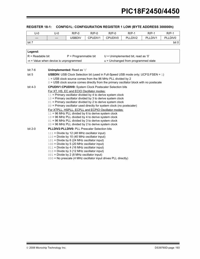
PIC18F2450/4450
© 2008 Microchip Technology Inc. DS39760D-page 193
REGISTER 18-1: CONFIG1L: CONFIGURATION REGISTER 1 LOW (BYTE ADDRESS 300000h)
U-0 U-0 R/P-0 R/P-0 R/P-0 R/P-1 R/P-1 R/P-1� � USBDIV CPUDIV1 CPUDIV0 PLLDIV2 PLLDIV1 PLLDIV0
bit 7 bit 0
Legend:R = Readable bit P = Programmable bit U = Unimplemented bit, read as �0�-n = Value when device is unprogrammed u = Unchanged from programmed state
bit 7-6 Unimplemented: Read as �0�bit 5 USBDIV: USB Clock Selection bit (used in Full-Speed USB mode only; UCFG:FSEN = 1)
1 = USB clock source comes from the 96 MHz PLL divided by 20 = USB clock source comes directly from the primary oscillator block with no postscale
bit 4-3 CPUDIV1:CPUDIV0: System Clock Postscaler Selection bitsFor XT, HS, EC and ECIO Oscillator modes:11 = Primary oscillator divided by 4 to derive system clock10 = Primary oscillator divided by 3 to derive system clock01 = Primary oscillator divided by 2 to derive system clock00 = Primary oscillator used directly for system clock (no postscaler)For XTPLL, HSPLL, ECPLL and ECPIO Oscillator modes:11 = 96 MHz PLL divided by 6 to derive system clock10 = 96 MHz PLL divided by 4 to derive system clock01 = 96 MHz PLL divided by 3 to derive system clock00 = 96 MHz PLL divided by 2 to derive system clock
bit 2-0 PLLDIV2:PLLDIV0: PLL Prescaler Selection bits111 = Divide by 12 (48 MHz oscillator input)110 = Divide by 10 (40 MHz oscillator input)101 = Divide by 6 (24 MHz oscillator input)100 = Divide by 5 (20 MHz oscillator input)011 = Divide by 4 (16 MHz oscillator input)010 = Divide by 3 (12 MHz oscillator input)001 = Divide by 2 (8 MHz oscillator input)000 = No prescale (4 MHz oscillator input drives PLL directly)
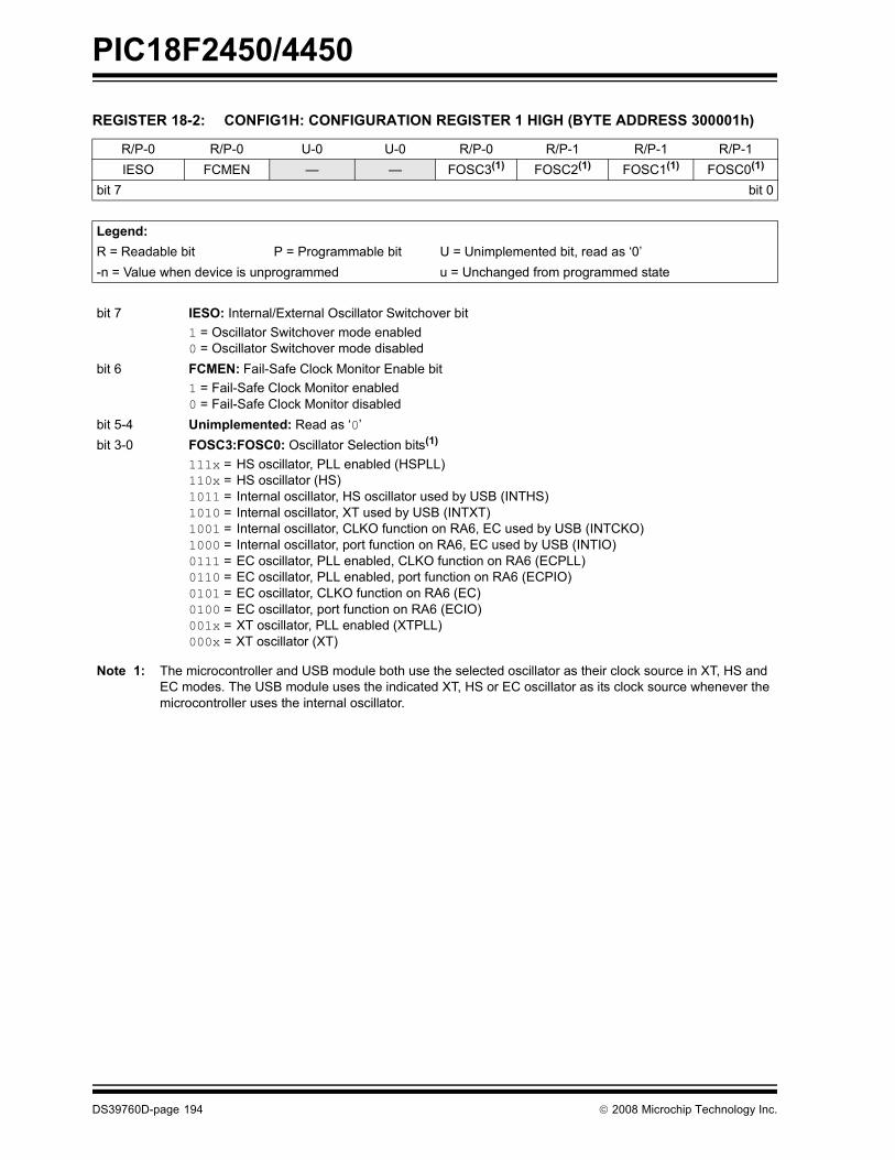
PIC18F2450/4450
DS39760D-page 194 © 2008 Microchip Technology Inc.
REGISTER 18-2: CONFIG1H: CONFIGURATION REGISTER 1 HIGH (BYTE ADDRESS 300001h)
R/P-0 R/P-0 U-0 U-0 R/P-0 R/P-1 R/P-1 R/P-1IESO FCMEN � � FOSC3(1) FOSC2(1) FOSC1(1) FOSC0(1)
bit 7 bit 0
Legend:R = Readable bit P = Programmable bit U = Unimplemented bit, read as �0�-n = Value when device is unprogrammed u = Unchanged from programmed state
bit 7 IESO: Internal/External Oscillator Switchover bit1 = Oscillator Switchover mode enabled0 = Oscillator Switchover mode disabled
bit 6 FCMEN: Fail-Safe Clock Monitor Enable bit1 = Fail-Safe Clock Monitor enabled0 = Fail-Safe Clock Monitor disabled
bit 5-4 Unimplemented: Read as �0�bit 3-0 FOSC3:FOSC0: Oscillator Selection bits(1)
111x = HS oscillator, PLL enabled (HSPLL)110x = HS oscillator (HS)1011 = Internal oscillator, HS oscillator used by USB (INTHS)1010 = Internal oscillator, XT used by USB (INTXT)1001 = Internal oscillator, CLKO function on RA6, EC used by USB (INTCKO)1000 = Internal oscillator, port function on RA6, EC used by USB (INTIO)0111 = EC oscillator, PLL enabled, CLKO function on RA6 (ECPLL)0110 = EC oscillator, PLL enabled, port function on RA6 (ECPIO)0101 = EC oscillator, CLKO function on RA6 (EC)0100 = EC oscillator, port function on RA6 (ECIO)001x = XT oscillator, PLL enabled (XTPLL)000x = XT oscillator (XT)
Note 1: The microcontroller and USB module both use the selected oscillator as their clock source in XT, HS and EC modes. The USB module uses the indicated XT, HS or EC oscillator as its clock source whenever the microcontroller uses the internal oscillator.
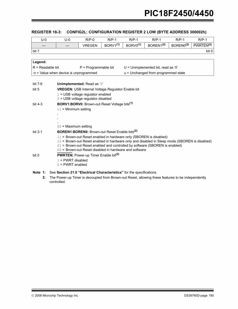
PIC18F2450/4450
© 2008 Microchip Technology Inc. DS39760D-page 195
REGISTER 18-3: CONFIG2L: CONFIGURATION REGISTER 2 LOW (BYTE ADDRESS 300002h)
U-0 U-0 R/P-0 R/P-1 R/P-1 R/P-1 R/P-1 R/P-1
� � VREGEN BORV1(1) BORV0(1) BOREN1(2) BOREN0(2) PWRTEN(2)
bit 7 bit 0
Legend:R = Readable bit P = Programmable bit U = Unimplemented bit, read as �0�-n = Value when device is unprogrammed u = Unchanged from programmed state
bit 7-6 Unimplemented: Read as �0�bit 5 VREGEN: USB Internal Voltage Regulator Enable bit
1 = USB voltage regulator enabled0 = USB voltage regulator disabled
bit 4-3 BORV1:BORV0: Brown-out Reset Voltage bits(1)
11 = Minimum setting ... 00 = Maximum setting
bit 2-1 BOREN1:BOREN0: Brown-out Reset Enable bits(2)
11 = Brown-out Reset enabled in hardware only (SBOREN is disabled)10 = Brown-out Reset enabled in hardware only and disabled in Sleep mode (SBOREN is disabled) 01 = Brown-out Reset enabled and controlled by software (SBOREN is enabled) 00 = Brown-out Reset disabled in hardware and software
bit 0 PWRTEN: Power-up Timer Enable bit(2)
1 = PWRT disabled 0 = PWRT enabled
Note 1: See Section 21.0 �Electrical Characteristics� for the specifications.2: The Power-up Timer is decoupled from Brown-out Reset, allowing these features to be independently
controlled.

PIC18F2450/4450
DS39760D-page 196 © 2008 Microchip Technology Inc.
REGISTER 18-4: CONFIG2H: CONFIGURATION REGISTER 2 HIGH (BYTE ADDRESS 300003h)
U-0 U-0 U-0 R/P-1 R/P-1 R/P-1 R/P-1 R/P-1
� � � WDTPS3 WDTPS2 WDTPS1 WDTPS0 WDTEN
bit 7 bit 0
Legend:R = Readable bit P = Programmable bit U = Unimplemented bit, read as �0�-n = Value when device is unprogrammed u = Unchanged from programmed state
bit 7-5 Unimplemented: Read as �0�bit 4-1 WDTPS3:WDTPS0: Watchdog Timer Postscale Select bits
1111 = 1:32,7681110 = 1:16,3841101 = 1:8,1921100 = 1:4,0961011 = 1:2,0481010 = 1:1,0241001 = 1:5121000 = 1:2560111 = 1:1280110 = 1:640101 = 1:320100 = 1:160011 = 1:80010 = 1:40001 = 1:20000 = 1:1
bit 0 WDTEN: Watchdog Timer Enable bit1 = WDT enabled0 = WDT disabled (control is placed on the SWDTEN bit)

PIC18F2450/4450
© 2008 Microchip Technology Inc. DS39760D-page 197
REGISTER 18-5: CONFIG3H: CONFIGURATION REGISTER 3 HIGH (BYTE ADDRESS 300005h)
R/P-1 U-0 U-0 U-0 U-0 R/P-0 R/P-1 U-0MCLRE � � � � LPT1OSC PBADEN �
bit 7 bit 0
Legend:R = Readable bit P = Programmable bit U = Unimplemented bit, read as �0�-n = Value when device is unprogrammed u = Unchanged from programmed state
bit 7 MCLRE: MCLR Pin Enable bit1 = MCLR pin enabled, RA5 input pin disabled0 = RA5 input pin enabled, MCLR pin disabled
bit 6-3 Unimplemented: Read as �0�bit 2 LPT1OSC: Low-Power Timer1 Oscillator Enable bit
1 = Timer1 configured for low-power operation0 = Timer1 configured for higher power operation
bit 1 PBADEN: PORTB A/D Enable bit (Affects ADCON1 Reset state. ADCON1 controls PORTB<4:0> pin configuration.)1 = PORTB<4:0> pins are configured as analog input channels on Reset0 = PORTB<4:0> pins are configured as digital I/O on Reset
bit 0 Unimplemented: Read as �0�

PIC18F2450/4450
DS39760D-page 198 © 2008 Microchip Technology Inc.
REGISTER 18-6: CONFIG4L: CONFIGURATION REGISTER 4 LOW (BYTE ADDRESS 300006h)
R/P-1 R/P-0 R/P-0 U-0 R/P-0 R/P-1 U-0 R/P-1
DEBUG XINST ICPRT(1) � BBSIZ LVP � STVRENbit 7 bit 0
Legend:R = Readable bit P = Programmable bit U = Unimplemented bit, read as �0�-n = Value when device is unprogrammed u = Unchanged from programmed state
bit 7 DEBUG: Background Debugger Enable bit1 = Background debugger disabled, RB6 and RB7 configured as general purpose I/O pins 0 = Background debugger enabled, RB6 and RB7 are dedicated to In-Circuit Debug
bit 6 XINST: Extended Instruction Set Enable bit1 = Instruction set extension and Indexed Addressing mode enabled 0 = Instruction set extension and Indexed Addressing mode disabled (Legacy mode)
bit 5 ICPRT: Dedicated In-Circuit Debug/Programming Port (ICPORT) Enable bit(1)
1 = ICPORT enabled0 = ICPORT disabled
bit 4 Unimplemented: Read as �0�bit 3 BBSIZ: Boot Block Size Select bit
1 = 2 kW boot block size 0 = 1 kW boot block size
bit 2 LVP: Single-Supply ICSP� Enable bit1 = Single-Supply ICSP enabled 0 = Single-Supply ICSP disabled
bit 1 Unimplemented: Read as �0�bit 0 STVREN: Stack Full/Underflow Reset Enable bit
1 = Stack full/underflow will cause Reset 0 = Stack full/underflow will not cause Reset
Note 1: Available only on PIC18F4450 devices in 44-pin TQFP packages. Always leave this bit clear in all other devices.

PIC18F2450/4450
© 2008 Microchip Technology Inc. DS39760D-page 199
REGISTER 18-7: CONFIG5L: CONFIGURATION REGISTER 5 LOW (BYTE ADDRESS 300008h)
U-0 U-0 U-0 U-0 U-0 U-0 R/C-1 R/C-1� � � � � � CP1 CP0
bit 7 bit 0
Legend:R = Readable bit C = Clearable bit U = Unimplemented bit, read as �0�-n = Value when device is unprogrammed u = Unchanged from programmed state
bit 7-2 Unimplemented: Read as �0�bit 1 CP1: Code Protection bit
1 = Block 1 (002000-003FFFh) is not code-protected 0 = Block 1 (002000-003FFFh) is code-protected
bit 0 CP0: Code Protection bit1 = Block 0 (000800-001FFFh) or (001000-001FFFh) is not code-protected 0 = Block 0 (000800-001FFFh) or (001000-001FFFh) is code-protected
REGISTER 18-8: CONFIG5H: CONFIGURATION REGISTER 5 HIGH (BYTE ADDRESS 300009h)
U-0 R/C-1 U-0 U-0 U-0 U-0 U-0 U-0� CPB � � � � � �
bit 7 bit 0
Legend:R = Readable bit C = Clearable bit U = Unimplemented bit, read as �0�-n = Value when device is unprogrammed u = Unchanged from programmed state
bit 7 Unimplemented: Read as �0�bit 6 CPB: Boot Block Code Protection bit
1 = Boot block (000000-0007FFh) or (000000-000FFFh) is not code-protected0 = Boot block (000000-0007FFh) or (000000-000FFFh) is code-protected
bit 5-0 Unimplemented: Read as �0�

PIC18F2450/4450
DS39760D-page 200 © 2008 Microchip Technology Inc.
REGISTER 18-9: CONFIG6L: CONFIGURATION REGISTER 6 LOW (BYTE ADDRESS 30000Ah)
U-0 U-0 U-0 U-0 U-0 U-0 R/C-1 R/C-1� � � � � � WRT1 WRT0
bit 7 bit 0
Legend:R = Readable bit C = Clearable bit U = Unimplemented bit, read as �0�-n = Value when device is unprogrammed u = Unchanged from programmed state
bit 7-2 Unimplemented: Read as �0�bit 1 WRT1: Write Protection bit
1 = Block 1 (002000-003FFFh) is not write-protected 0 = Block 1 (002000-003FFFh) is write-protected
bit 0 WRT0: Write Protection bit1 = Block 0 (000800-001FFFh) or (001000-001FFFh) is not write-protected 0 = Block 0 (000800-001FFFh) or (001000-001FFFh) is write-protected
REGISTER 18-10: CONFIG6H: CONFIGURATION REGISTER 6 HIGH (BYTE ADDRESS 30000Bh)
U-0 R/C-1 R-1 U-0 U-0 U-0 U-0 U-0� WRTB WRTC(1) � � � � �
bit 7 bit 0
Legend:R = Readable bit C = Clearable bit U = Unimplemented bit, read as �0�-n = Value when device is unprogrammed u = Unchanged from programmed state
bit 7 Unimplemented: Read as �0�bit 6 WRTB: Boot Block Write Protection bit
1 = Boot block (000000-0007FFh) or (000000-000FFFh) is not write-protected0 = Boot block (000000-0007FFh) or (000000-000FFFh) is write-protected
bit 5 WRTC: Configuration Register Write Protection bit(1)
1 = Configuration registers (300000-3000FFh) are not write-protected0 = Configuration registers (300000-3000FFh) are write-protected
bit 4-0 Unimplemented: Read as �0�
Note 1: This bit is read-only in normal execution mode; it can be written only in Program mode.
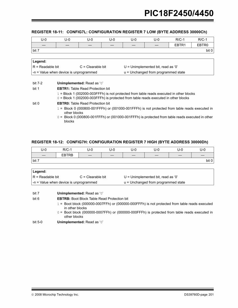
PIC18F2450/4450
© 2008 Microchip Technology Inc. DS39760D-page 201
REGISTER 18-11: CONFIG7L: CONFIGURATION REGISTER 7 LOW (BYTE ADDRESS 30000Ch)
U-0 U-0 U-0 U-0 U-0 U-0 R/C-1 R/C-1� � � � � � EBTR1 EBTR0
bit 7 bit 0
Legend:R = Readable bit C = Clearable bit U = Unimplemented bit, read as �0�-n = Value when device is unprogrammed u = Unchanged from programmed state
bit 7-2 Unimplemented: Read as �0�bit 1 EBTR1: Table Read Protection bit
1 = Block 1 (002000-003FFFh) is not protected from table reads executed in other blocks 0 = Block 1 (002000-003FFFh) is protected from table reads executed in other blocks
bit 0 EBTR0: Table Read Protection bit1 = Block 0 (000800-001FFFh) or (001000-001FFFh) is not protected from table reads executed in
other blocks 0 = Block 0 (000800-001FFFh) or (001000-001FFFh) is protected from table reads executed in other
blocks
REGISTER 18-12: CONFIG7H: CONFIGURATION REGISTER 7 HIGH (BYTE ADDRESS 30000Dh)
U-0 R/C-1 U-0 U-0 U-0 U-0 U-0 U-0� EBTRB � � � � � �
bit 7 bit 0
Legend:R = Readable bit C = Clearable bit U = Unimplemented bit, read as �0�-n = Value when device is unprogrammed u = Unchanged from programmed state
bit 7 Unimplemented: Read as �0�bit 6 EBTRB: Boot Block Table Read Protection bit
1 = Boot block (000000-0007FFh) or (000000-000FFFh) is not protected from table reads executedin other blocks
0 = Boot block (000000-0007FFh) or (000000-000FFFh) is protected from table reads executed inother blocks
bit 5-0 Unimplemented: Read as �0�

PIC18F2450/4450
DS39760D-page 202 © 2008 Microchip Technology Inc.
REGISTER 18-13: DEVID1: DEVICE ID REGISTER 1 FOR PIC18F2450/4450 DEVICES
R R R R R R R RDEV2 DEV1 DEV0 REV4 REV3 REV2 REV1 REV0
bit 7 bit 0
Legend:R = Read-only bit P = Programmable bit U = Unimplemented bit, read as �0�-n = Value when device is unprogrammed u = Unchanged from programmed state
bit 7-5 DEV2:DEV0: Device ID bits001 = PIC18F2450000 = PIC18F4450
bit 4-0 REV4:REV0: Revision ID bitsThese bits are used to indicate the device revision.
REGISTER 18-14: DEVID2: DEVICE ID REGISTER 2 FOR PIC18F2450/4450 DEVICES
R R R R R R R RDEV10(1) DEV9(1) DEV8(1) DEV7(1) DEV6(1) DEV5(1) DEV4(1) DEV3(1)
bit 7 bit 0
Legend:R = Read-only bit P = Programmable bit U = Unimplemented bit, read as �0�-n = Value when device is unprogrammed u = Unchanged from programmed state
bit 7-0 DEV10:DEV3: Device ID bits(1)
These bits are used with the DEV2:DEV0 bits in the DEVID1 register to identify the part number.0010 0100 = PIC18F2450/4450 devices
Note 1: These values for DEV10:DEV3 may be shared with other devices. The specific device is always identified by using the entire DEV10:DEV0 bit sequence.

PIC18F2450/4450
© 2008 Microchip Technology Inc. DS39760D-page 203
18.2 Watchdog Timer (WDT)For PIC18F2450/4450 devices, the WDT is driven bythe INTRC source. When the WDT is enabled, theclock source is also enabled. The nominal WDT periodis 4 ms and has the same stability as the INTRCoscillator.
The 4 ms period of the WDT is multiplied by a 16-bitpostscaler. Any output of the WDT postscaler isselected by a multiplexer, controlled by bits inConfiguration Register 2H. Available periods rangefrom 4 ms to 131.072 seconds (2.18 minutes). TheWDT and postscaler are cleared when any of thefollowing events occur: a SLEEP or CLRWDT instructionis executed or a clock failure has occurred.
18.2.1 CONTROL REGISTER
Register 18-15 shows the WDTCON register. This is areadable and writable register which contains a controlbit that allows software to override the WDT enableConfiguration bit, but only if the Configuration bit hasdisabled the WDT.
FIGURE 18-1: WDT BLOCK DIAGRAM
Note 1: The CLRWDT and SLEEP instructionsclear the WDT and postscaler countswhen executed.
2: When a CLRWDT instruction is executed,the postscaler count will be cleared.
INTRC Source
WDT
Wake-up from
Reset
WDT
WDT Counter
Programmable Postscaler1:1 to 1:32,768
Enable WDT
WDTPS<3:0>
SWDTENWDTEN
CLRWDT
4
Power-Managed
ResetAll Device Resets
SLEEP
INTRC Control
÷128
Modes
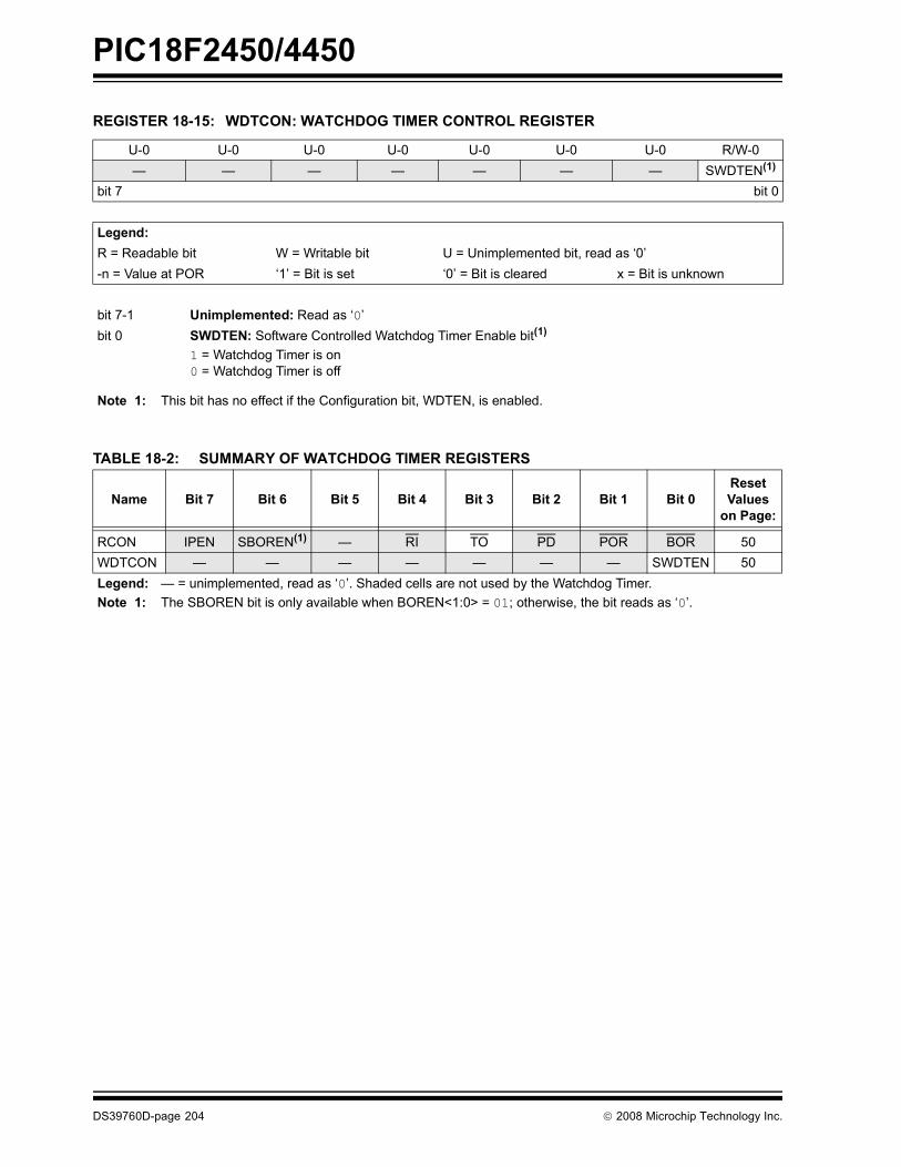
PIC18F2450/4450
DS39760D-page 204 © 2008 Microchip Technology Inc.
TABLE 18-2: SUMMARY OF WATCHDOG TIMER REGISTERS
REGISTER 18-15: WDTCON: WATCHDOG TIMER CONTROL REGISTER
U-0 U-0 U-0 U-0 U-0 U-0 U-0 R/W-0� � � � � � � SWDTEN(1)
bit 7 bit 0
Legend:R = Readable bit W = Writable bit U = Unimplemented bit, read as �0�-n = Value at POR �1� = Bit is set �0� = Bit is cleared x = Bit is unknown
bit 7-1 Unimplemented: Read as �0�bit 0 SWDTEN: Software Controlled Watchdog Timer Enable bit(1)
1 = Watchdog Timer is on0 = Watchdog Timer is off
Note 1: This bit has no effect if the Configuration bit, WDTEN, is enabled.
Name Bit 7 Bit 6 Bit 5 Bit 4 Bit 3 Bit 2 Bit 1 Bit 0Reset Values
on Page:
RCON IPEN SBOREN(1) � RI TO PD POR BOR 50WDTCON � � � � � � � SWDTEN 50Legend: � = unimplemented, read as �0�. Shaded cells are not used by the Watchdog Timer.Note 1: The SBOREN bit is only available when BOREN<1:0> = 01; otherwise, the bit reads as �0�.
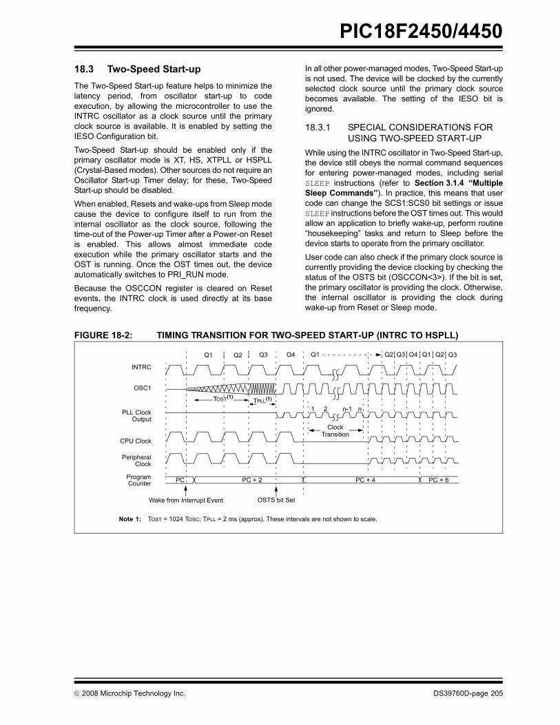
PIC18F2450/4450
© 2008 Microchip Technology Inc. DS39760D-page 205
18.3 Two-Speed Start-upThe Two-Speed Start-up feature helps to minimize thelatency period, from oscillator start-up to codeexecution, by allowing the microcontroller to use theINTRC oscillator as a clock source until the primaryclock source is available. It is enabled by setting theIESO Configuration bit.
Two-Speed Start-up should be enabled only if theprimary oscillator mode is XT, HS, XTPLL or HSPLL(Crystal-Based modes). Other sources do not require anOscillator Start-up Timer delay; for these, Two-SpeedStart-up should be disabled.
When enabled, Resets and wake-ups from Sleep modecause the device to configure itself to run from theinternal oscillator as the clock source, following thetime-out of the Power-up Timer after a Power-on Resetis enabled. This allows almost immediate codeexecution while the primary oscillator starts and theOST is running. Once the OST times out, the deviceautomatically switches to PRI_RUN mode.
Because the OSCCON register is cleared on Resetevents, the INTRC clock is used directly at its basefrequency.
In all other power-managed modes, Two-Speed Start-upis not used. The device will be clocked by the currentlyselected clock source until the primary clock sourcebecomes available. The setting of the IESO bit isignored.
18.3.1 SPECIAL CONSIDERATIONS FOR USING TWO-SPEED START-UP
While using the INTRC oscillator in Two-Speed Start-up,the device still obeys the normal command sequencesfor entering power-managed modes, including serialSLEEP instructions (refer to Section 3.1.4 �MultipleSleep Commands�). In practice, this means that usercode can change the SCS1:SCS0 bit settings or issueSLEEP instructions before the OST times out. This wouldallow an application to briefly wake-up, perform routine�housekeeping� tasks and return to Sleep before thedevice starts to operate from the primary oscillator.
User code can also check if the primary clock source iscurrently providing the device clocking by checking thestatus of the OSTS bit (OSCCON<3>). If the bit is set,the primary oscillator is providing the clock. Otherwise,the internal oscillator is providing the clock duringwake-up from Reset or Sleep mode.
FIGURE 18-2: TIMING TRANSITION FOR TWO-SPEED START-UP (INTRC TO HSPLL)
Q1 Q3 Q4
OSC1
Peripheral
Program PC PC + 2
INTRC
PLL Clock
Q1
PC + 6
Q2
Output
Q3 Q4 Q1
CPU Clock
PC + 4
Clock
Counter
Q2 Q2 Q3
Note 1: TOST = 1024 TOSC; TPLL = 2 ms (approx). These intervals are not shown to scale.
Wake from Interrupt Event
TPLL(1)
1 2 n-1 n
Clock
OSTS bit Set
Transition
TOST(1)
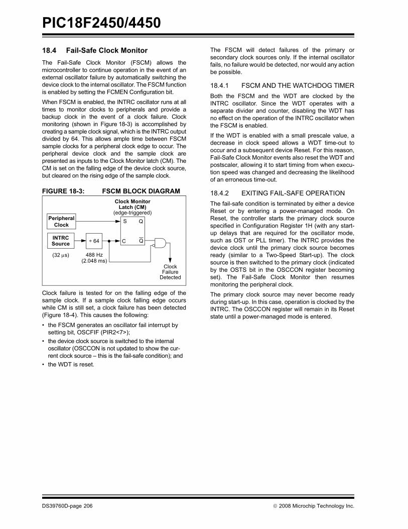
PIC18F2450/4450
DS39760D-page 206 © 2008 Microchip Technology Inc.
18.4 Fail-Safe Clock MonitorThe Fail-Safe Clock Monitor (FSCM) allows themicrocontroller to continue operation in the event of anexternal oscillator failure by automatically switching thedevice clock to the internal oscillator. The FSCM functionis enabled by setting the FCMEN Configuration bit.
When FSCM is enabled, the INTRC oscillator runs at alltimes to monitor clocks to peripherals and provide abackup clock in the event of a clock failure. Clockmonitoring (shown in Figure 18-3) is accomplished bycreating a sample clock signal, which is the INTRC outputdivided by 64. This allows ample time between FSCMsample clocks for a peripheral clock edge to occur. Theperipheral device clock and the sample clock arepresented as inputs to the Clock Monitor latch (CM). TheCM is set on the falling edge of the device clock source,but cleared on the rising edge of the sample clock.
FIGURE 18-3: FSCM BLOCK DIAGRAM
Clock failure is tested for on the falling edge of thesample clock. If a sample clock falling edge occurswhile CM is still set, a clock failure has been detected(Figure 18-4). This causes the following:
� the FSCM generates an oscillator fail interrupt by setting bit, OSCFIF (PIR2<7>);
� the device clock source is switched to the internal oscillator (OSCCON is not updated to show the cur-rent clock source � this is the fail-safe condition); and
� the WDT is reset.
The FSCM will detect failures of the primary orsecondary clock sources only. If the internal oscillatorfails, no failure would be detected, nor would any actionbe possible.
18.4.1 FSCM AND THE WATCHDOG TIMERBoth the FSCM and the WDT are clocked by theINTRC oscillator. Since the WDT operates with aseparate divider and counter, disabling the WDT hasno effect on the operation of the INTRC oscillator whenthe FSCM is enabled.
If the WDT is enabled with a small prescale value, adecrease in clock speed allows a WDT time-out tooccur and a subsequent device Reset. For this reason,Fail-Safe Clock Monitor events also reset the WDT andpostscaler, allowing it to start timing from when execu-tion speed was changed and decreasing the likelihoodof an erroneous time-out.
18.4.2 EXITING FAIL-SAFE OPERATIONThe fail-safe condition is terminated by either a deviceReset or by entering a power-managed mode. OnReset, the controller starts the primary clock sourcespecified in Configuration Register 1H (with any start-up delays that are required for the oscillator mode,such as OST or PLL timer). The INTRC provides thedevice clock until the primary clock source becomesready (similar to a Two-Speed Start-up). The clocksource is then switched to the primary clock (indicatedby the OSTS bit in the OSCCON register becomingset). The Fail-Safe Clock Monitor then resumesmonitoring the peripheral clock.
The primary clock source may never become readyduring start-up. In this case, operation is clocked by theINTRC. The OSCCON register will remain in its Resetstate until a power-managed mode is entered.
Peripheral
INTRC ÷ 64
S
C
Q
(32 μs) 488 Hz(2.048 ms)
Clock MonitorLatch (CM)
(edge-triggered)
ClockFailure
Detected
Source
Clock
Q
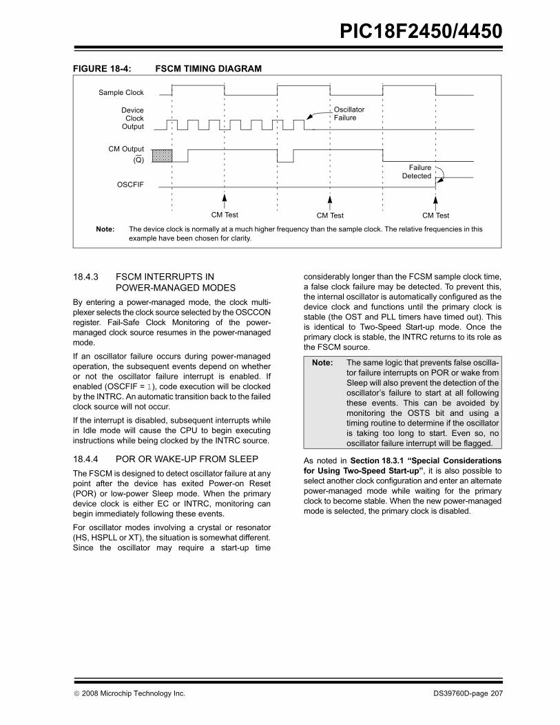
PIC18F2450/4450
© 2008 Microchip Technology Inc. DS39760D-page 207
FIGURE 18-4: FSCM TIMING DIAGRAM
18.4.3 FSCM INTERRUPTS IN POWER-MANAGED MODES
By entering a power-managed mode, the clock multi-plexer selects the clock source selected by the OSCCONregister. Fail-Safe Clock Monitoring of the power-managed clock source resumes in the power-managedmode.
If an oscillator failure occurs during power-managedoperation, the subsequent events depend on whetheror not the oscillator failure interrupt is enabled. Ifenabled (OSCFIF = 1), code execution will be clockedby the INTRC. An automatic transition back to the failedclock source will not occur.
If the interrupt is disabled, subsequent interrupts whilein Idle mode will cause the CPU to begin executinginstructions while being clocked by the INTRC source.
18.4.4 POR OR WAKE-UP FROM SLEEPThe FSCM is designed to detect oscillator failure at anypoint after the device has exited Power-on Reset(POR) or low-power Sleep mode. When the primarydevice clock is either EC or INTRC, monitoring canbegin immediately following these events.
For oscillator modes involving a crystal or resonator(HS, HSPLL or XT), the situation is somewhat different.Since the oscillator may require a start-up time
considerably longer than the FCSM sample clock time,a false clock failure may be detected. To prevent this,the internal oscillator is automatically configured as thedevice clock and functions until the primary clock isstable (the OST and PLL timers have timed out). Thisis identical to Two-Speed Start-up mode. Once theprimary clock is stable, the INTRC returns to its role asthe FSCM source.
As noted in Section 18.3.1 �Special Considerationsfor Using Two-Speed Start-up�, it is also possible toselect another clock configuration and enter an alternatepower-managed mode while waiting for the primaryclock to become stable. When the new power-managedmode is selected, the primary clock is disabled.
OSCFIF
CM Output
DeviceClock
Output
Sample Clock
FailureDetected
OscillatorFailure
Note: The device clock is normally at a much higher frequency than the sample clock. The relative frequencies in thisexample have been chosen for clarity.
(Q)
CM Test CM Test CM Test
Note: The same logic that prevents false oscilla-tor failure interrupts on POR or wake fromSleep will also prevent the detection of theoscillator�s failure to start at all followingthese events. This can be avoided bymonitoring the OSTS bit and using atiming routine to determine if the oscillatoris taking too long to start. Even so, nooscillator failure interrupt will be flagged.

PIC18F2450/4450
DS39760D-page 208 © 2008 Microchip Technology Inc.
18.5 Program Verification and Code Protection
The overall structure of the code protection on thePIC18 Flash devices differs significantly from otherPIC® microcontrollers.
The user program memory is divided into three blocks.One of these is a boot block of 1 or 2 Kbytes. Theremainder of the memory is divided into two blocks onbinary boundaries.
Each of the three blocks has three code protection bitsassociated with them. They are:
� Code-Protect bit (CPx)� Write-Protect bit (WRTx)� External Block Table Read bit (EBTRx)
Figure 18-5 shows the program memory organizationfor 24 and 32-Kbyte devices and the specific codeprotection bit associated with each block. The actuallocations of the bits are summarized in Table 18-3.
FIGURE 18-5: CODE-PROTECTED PROGRAM MEMORY FOR PIC18F2450/4450
TABLE 18-3: SUMMARY OF CODE PROTECTION REGISTERSFile Name Bit 7 Bit 6 Bit 5 Bit 4 Bit 3 Bit 2 Bit 1 Bit 0
300008h CONFIG5L � � � � � � CP1 CP0300009h CONFIG5H � CPB � � � � � �30000Ah CONFIG6L � � � � � � WRT1 WRT030000Bh CONFIG6H � WRTB WRTC � � � � �30000Ch CONFIG7L � � � � � � EBTR1 EBTR030000Dh CONFIG7H � EBTRB � � � � � �Legend: Shaded cells are unimplemented.
MEMORY SIZE/DEVICE Block Code Protection
Controlled By:16 Kbytes(PIC18F2450/4450)
Address Range
Boot Block000000h0007FFh000FFFh
CPB, WRTB, EBTRB
Block 0001000h
001FFFhCP0, WRT0, EBTR0
Block 1002000h
003FFFhCP1, WRT1, EBTR1
UnimplementedRead �0�s
UnimplementedRead �0�s
UnimplementedRead �0�s
1FFFFFh
(Unimplemented Memory Space)

PIC18F2450/4450
© 2008 Microchip Technology Inc. DS39760D-page 209
18.5.1 PROGRAM MEMORYCODE PROTECTION
The program memory may be read to or written fromany location using the table read and table writeinstructions. The device ID may be read with tablereads. The Configuration registers may be read andwritten with the table read and table write instructions.
In normal execution mode, the CPx bits have no directeffect. CPx bits inhibit external reads and writes. Ablock of user memory may be protected from tablewrites if the WRTx Configuration bit is �0�. The EBTRxbits control table reads. For a block of user memorywith the EBTRx bit set to �0�, a table read instructionthat executes from within that block is allowed to read.
A table read instruction that executes from a locationoutside of that block is not allowed to read and willresult in reading �0�s. Figure 18-6 through Figure 18-8illustrate table write and table read protection.
FIGURE 18-6: TABLE WRITE (WRTx) DISALLOWED
Note: Code protection bits may only be written toa �0� from a �1� state. It is not possible towrite a �1� to a bit in the �0� state. Codeprotection bits are only set to �1� by a fullChip Erase or Block Erase function. Thefull Chip Erase and Block Erase functionscan only be initiated via ICSP operation oran external programmer.
000000h
000FFFh001000h
001FFFh002000h
003FFFh
WRTB, EBTRB = 11
WRT0, EBTR0 = 01
WRT1, EBTR1 = 11
WRT2, EBTR2 = 11
WRT3, EBTR3 = 11
TBLWT*
TBLPTR = 0008FFhPC = 001FFEh
Register Values Program Memory Configuration Bit Settings
Results: All table writes disabled to Blockn whenever WRTx = 0.
0007FFh
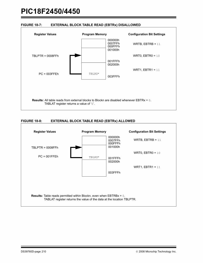
PIC18F2450/4450
DS39760D-page 210 © 2008 Microchip Technology Inc.
FIGURE 18-7: EXTERNAL BLOCK TABLE READ (EBTRx) DISALLOWED
FIGURE 18-8: EXTERNAL BLOCK TABLE READ (EBTRx) ALLOWED
WRTB, EBTRB = 11
WRT0, EBTR0 = 10
WRT1, EBTR1 = 11TBLRD*
TBLPTR = 0008FFh
PC = 003FFEh
Results: All table reads from external blocks to Blockn are disabled whenever EBTRx = 0.TABLAT register returns a value of �0�.
Register Values Program Memory Configuration Bit Settings
000000h
000FFFh001000h
001FFFh002000h
003FFFh
0007FFh
WRTB, EBTRB = 11
WRT0, EBTR0 = 10
WRT1, EBTR1 = 11
TBLRD*
TBLPTR = 0008FFh
PC = 001FFEh
Register Values Program Memory Configuration Bit Settings
Results: Table reads permitted within Blockn, even when EBTRBx = 0.TABLAT register returns the value of the data at the location TBLPTR.
000000h
000FFFh001000h
001FFFh002000h
003FFFh
0007FFh
PIC18F2450/4450
© 2008 Microchip Technology Inc. DS39760D-page 211
18.5.2 CONFIGURATION REGISTER PROTECTION
The Configuration registers can be write-protected.The WRTC bit controls protection of the Configurationregisters. In normal execution mode, the WRTC bit isreadable only. WRTC can only be written via ICSPoperation or an external programmer.
18.6 ID LocationsEight memory locations (200000h-200007h) aredesignated as ID locations, where the user can storechecksum or other code identification numbers. Theselocations are both readable and writable during normalexecution through the TBLRD and TBLWT instructionsor during program/verify. The ID locations can be readwhen the device is code-protected.
18.7 In-Circuit Serial ProgrammingPIC18F2450/4450 microcontrollers can be seriallyprogrammed while in the end application circuit. This issimply done with two lines for clock and data and threeother lines for power, ground and the programmingvoltage. This allows customers to manufacture boardswith unprogrammed devices and then program themicrocontroller just before shipping the product. Thisalso allows the most recent firmware or a customfirmware to be programmed.
18.8 In-Circuit DebuggerWhen the DEBUG Configuration bit is programmed toa �0�, the In-Circuit Debugger functionality is enabled.This function allows simple debugging functions whenused with MPLAB® IDE. When the microcontroller hasthis feature enabled, some resources are not availablefor general use. Table 18-4 shows which resources arerequired by the background debugger.
TABLE 18-4: DEBUGGER RESOURCES
To use the In-Circuit Debugger function of themicrocontroller, the design must implement In-CircuitSerial Programming connections to MCLR/VPP/RE3,VDD, VSS, RB7 and RB6. This will interface to theIn-Circuit Debugger module available from Microchipor one of the third party development tool companies.
18.9 Special ICPORT Features (Designated Packages Only)
Under specific circumstances, the No Connect (NC)pins of PIC18F4450 devices in 44-pin TQFP packagescan provide additional functionality. These features arecontrolled by device Configuration bits and areavailable only in this package type and pin count.
18.9.1 DEDICATED ICD/ICSP PORTThe 44-pin TQFP devices can use NC pins to provide analternate port for In-Circuit Debugging (ICD) and In-Circuit Serial Programming (ICSP). These pins arecollectively known as the dedicated ICSP/ICD port, sincethey are not shared with any other function of the device.
When implemented, the dedicated port activates threeNC pins to provide an alternate device Reset, data andclock ports. None of these ports overlap with standardI/O pins, making the I/O pins available to the user�sapplication.
The dedicated ICSP/ICD port is enabled by setting theICPRT Configuration bit. The port functions the sameway as the legacy ICSP/ICD port on RB6/RB7.Table 18-5 identifies the functionally equivalent pins forICSP and ICD purposes.
TABLE 18-5: EQUIVALENT PINS FOR LEGACY AND DEDICATED ICD/ICSP� PORTS
I/O pins: RB6, RB7Stack: 2 levelsProgram Memory: 512 bytesData Memory: 10 bytes
Pin NamePin
Type Pin FunctionLegacy Port
Dedicated Port
MCLR/VPP/RE3
NC/ICRST/ICVPP
P Device Reset and Programming Enable
RB6/KBI2/PGC
NC/ICCK/ICPGC
I Serial Clock
RB7/KBI3/PGD
NC/ICDT/ICPGD
I/O Serial Data
Legend: I = Input, O = Output, P = Power
PIC18F2450/4450
DS39760D-page 212 © 2008 Microchip Technology Inc.
Even when the dedicated port is enabled, the ICSP andICD functions remain available through the legacy port.When VIHH is seen on the MCLR/VPP/RE3 pin, thestate of the ICRST/ICVPP pin is ignored.
18.9.2 28-PIN EMULATIONPIC18F4450 devices in 44-pin TQFP packages alsohave the ability to change their configuration underexternal control for debugging purposes. This allowsthe device to behave as if it were a PIC18F2450/445028-pin device.
This 28-pin Configuration mode is controlled through asingle pin, NC/ICPORTS. Connecting this pin to VSSforces the device to function as a 28-pin device.Features normally associated with the 40/44-pindevices are disabled, along with their correspondingcontrol registers and bits. On the other hand,connecting the pin to VDD forces the device to functionin its default configuration.
The configuration option is only available whenbackground debugging and the dedicated ICD/ICSPport are both enabled (DEBUG Configuration bit isclear and ICPRT Configuration bit is set). Whendisabled, NC/ICPORTS is a No Connect pin.
18.10 Single-Supply ICSP ProgrammingThe LVP Configuration bit enables Single-SupplyICSP Programming (formerly known as Low-VoltageICSP Programming or LVP). When Single-SupplyProgramming is enabled, the microcontroller can beprogrammed without requiring high voltage beingapplied to the MCLR/VPP/RE3 pin, but the RB5/KBI1/PGM pin is then dedicated to controlling Programmode entry and is not available as a general purposeI/O pin.
While programming using Single-Supply Program-ming, VDD is applied to the MCLR/VPP/RE3 pin as innormal execution mode. To enter Programming mode,VDD is applied to the PGM pin.
If Single-Supply ICSP Programming mode will not beused, the LVP bit can be cleared. RB5/KBI1/PGM thenbecomes available as the digital I/O pin, RB5. The LVPbit may be set or cleared only when using standardhigh-voltage programming (VIHH applied to the MCLR/VPP/RE3 pin). Once LVP has been disabled, only thestandard high-voltage programming is available andmust be used to program the device.
Memory that is not code-protected can be erased usingeither a Block Erase, or erased row by row, then writtenat any specified VDD. If code-protected memory is to beerased, a Block Erase is required. If a Block Erase is tobe performed when using Low-Voltage Programming,the device must be supplied with VDD of 4.5V to 5.5V.
Note 1: The ICPRT Configuration bit can only beprogrammed through the default ICSPport.
2: The ICPRT Configuration bit must bemaintained clear for all 28-pin and 40-pindevices; otherwise, unexpected operationmay occur.
Note 1: High-Voltage Programming is alwaysavailable, regardless of the state of theLVP bit, by applying VIHH to the MCLR pin.
2: While in Low-Voltage ICSP Programmingmode, the RB5 pin can no longer be usedas a general purpose I/O pin and shouldbe held low during normal operation.
3: When using Low-Voltage ICSP Program-ming (LVP) and the pull-ups on PORTBare enabled, bit 5 in the TRISB registermust be cleared to disable the pull-up onRB5 and ensure the proper operation ofthe device.
4: If the device Master Clear is disabled,verify that either of the following is done toensure proper entry into ICSP mode:
a) Disable Low-Voltage Programming(CONFIG4L<2> = 0); or
b) Make certain that RB5/KBI1/PGMis held low during entry into ICSP.

PIC18F2450/4450
© 2008 Microchip Technology Inc. DS39760D-page 213
19.0 INSTRUCTION SET SUMMARYPIC18F2450/4450 devices incorporate the standardset of 75 PIC18 core instructions, as well as anextended set of eight new instructions for theoptimization of code that is recursive or that utilizes asoftware stack. The extended set is discussed later inthis section.
19.1 Standard Instruction SetThe standard PIC18 instruction set adds manyenhancements to the previous PIC MCU instructionsets, while maintaining an easy migration from thesePIC MCU instruction sets. Most instructions are asingle program memory word (16 bits) but there arefour instructions that require two program memorylocations.
Each single-word instruction is a 16-bit word dividedinto an opcode, which specifies the instruction type andone or more operands, which further specify theoperation of the instruction.
The instruction set is highly orthogonal and is groupedinto four basic categories:
� Byte-oriented operations� Bit-oriented operations� Literal operations� Control operations
The PIC18 instruction set summary in Table 19-2 listsbyte-oriented, bit-oriented, literal and controloperations. Table 19-1 shows the opcode fielddescriptions.
Most byte-oriented instructions have three operands:
1. The file register (specified by �f�) 2. The destination of the result (specified by �d�) 3. The accessed memory (specified by �a�)
The file register designator, �f�, specifies which fileregister is to be used by the instruction. The destinationdesignator, �d�, specifies where the result of theoperation is to be placed. If �d� is �0�, the result is placedin the WREG register. If �d� is �1�, the result is placed inthe file register specified in the instruction.
All bit-oriented instructions have three operands:
1. The file register (specified by �f�) 2. The bit in the file register (specified by �b�) 3. The accessed memory (specified by �a�)
The bit field designator �b� selects the number of the bitaffected by the operation, while the file registerdesignator, �f�, represents the number of the file inwhich the bit is located.
The literal instructions may use some of the followingoperands:
� A literal value to be loaded into a file register (specified by �k�)
� The desired FSR register to load the literal value into (specified by �f�)
� No operand required (specified by ���)
The control instructions may use some of the followingoperands:
� A program memory address (specified by �n�)� The mode of the CALL or RETURN instructions
(specified by �s�)� The mode of the table read and table write
instructions (specified by �m�)� No operand required
(specified by ���)
All instructions are a single word, except for fourdouble-word instructions. These instructions weremade double-word to contain the required informationin 32 bits. In the second word, the 4 MSbs are �1�s. Ifthis second word is executed as an instruction (byitself), it will execute as a NOP.
All single-word instructions are executed in a singleinstruction cycle, unless a conditional test is true or theprogram counter is changed as a result of the instruc-tion. In these cases, the execution takes two instructioncycles with the additional instruction cycle(s) executedas a NOP.
The double-word instructions execute in two instructioncycles.
One instruction cycle consists of four oscillator periods.Thus, for an oscillator frequency of 4 MHz, the normalinstruction execution time is 1 μs. If a conditional test istrue, or the program counter is changed as a result ofan instruction, the instruction execution time is 2 μs.Two-word branch instructions (if true) would take 3 μs.
Figure 19-1 shows the general formats that theinstructions can have. All examples use the convention�nnh� to represent a hexadecimal number.
The instruction set summary, shown in Table 19-2, liststhe standard instructions recognized by the MicrochipMPASMTM Assembler.
Section 19.1.1 �Standard Instruction Set� providesa description of each instruction.
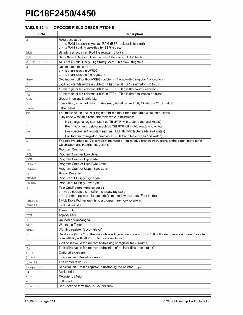
PIC18F2450/4450
DS39760D-page 214 © 2008 Microchip Technology Inc.
TABLE 19-1: OPCODE FIELD DESCRIPTIONS Field Description
a RAM access bita = 0: RAM location in Access RAM (BSR register is ignored)a = 1: RAM bank is specified by BSR register
bbb Bit address within an 8-bit file register (0 to 7).BSR Bank Select Register. Used to select the current RAM bank.C, DC, Z, OV, N ALU Status bits: Carry, Digit Carry, Zero, Overflow, Negative.d Destination select bit
d = 0: store result in WREGd = 1: store result in file register f
dest Destination: either the WREG register or the specified register file location.f 8-bit register file address (00h to FFh) or 2-bit FSR designator (0h to 3h).fs 12-bit register file address (000h to FFFh). This is the source address. fd 12-bit register file address (000h to FFFh). This is the destination address. GIE Global Interrupt Enable bit.k Literal field, constant data or label (may be either an 8-bit, 12-bit or a 20-bit value).label Label name.mm The mode of the TBLPTR register for the table read and table write instructions.
Only used with table read and table write instructions:* No change to register (such as TBLPTR with table reads and writes)*+ Post-Increment register (such as TBLPTR with table reads and writes)*- Post-Decrement register (such as TBLPTR with table reads and writes)+* Pre-Increment register (such as TBLPTR with table reads and writes)n The relative address (2�s complement number) for relative branch instructions or the direct address for
Call/Branch and Return instructions.PC Program Counter.PCL Program Counter Low Byte.PCH Program Counter High Byte.PCLATH Program Counter High Byte Latch.PCLATU Program Counter Upper Byte Latch.PD Power-Down bit.PRODH Product of Multiply High Byte.PRODL Product of Multiply Low Byte.s Fast Call/Return mode select bit
s = 0: do not update into/from shadow registerss = 1: certain registers loaded into/from shadow registers (Fast mode)
TBLPTR 21-bit Table Pointer (points to a program memory location).TABLAT 8-bit Table Latch.TO Time-out bit.TOS Top-of-Stack.u Unused or unchanged.WDT Watchdog Timer.WREG Working register (accumulator).x Don�t care (�0� or �1�). The assembler will generate code with x = 0. It is the recommended form of use for
compatibility with all Microchip software tools.zs 7-bit offset value for indirect addressing of register files (source).zd 7-bit offset value for indirect addressing of register files (destination).{ } Optional argument.[text] Indicates an indexed address.(text) The contents of text.[expr]<n> Specifies bit n of the register indicated by the pointer, expr.→ Assigned to.< > Register bit field.∈ In the set of.italics User-defined term (font is Courier New).

PIC18F2450/4450
© 2008 Microchip Technology Inc. DS39760D-page 215
FIGURE 19-1: GENERAL FORMAT FOR INSTRUCTIONS
Byte-oriented file register operations
15 10 9 8 7 0
d = 0 for result destination to be WREG register
OPCODE d a f (FILE #)
d = 1 for result destination to be file register (f)a = 0 to force Access Bank
Bit-oriented file register operations
15 12 11 9 8 7 0OPCODE b (BIT #) a f (FILE #)
b = 3-bit position of bit in file register (f)
Literal operations
15 8 7 0 OPCODE k (literal)
k = 8-bit immediate value
Byte to Byte move operations (2-word)
15 12 11 0OPCODE f (Source FILE #)
CALL, GOTO and Branch operations 15 8 7 0
OPCODE n<7:0> (literal)
n = 20-bit immediate value
a = 1 for BSR to select bankf = 8-bit file register address
a = 0 to force Access Banka = 1 for BSR to select bankf = 8-bit file register address
15 12 11 01111 n<19:8> (literal)
15 12 11 0 1111 f (Destination FILE #)
f = 12-bit file register address
Control operations
Example Instruction
ADDWF MYREG, W, B
MOVFF MYREG1, MYREG2
BSF MYREG, bit, B
MOVLW 7Fh
GOTO Label
15 8 7 0
OPCODE n<7:0> (literal)
15 12 11 0
1111 n<19:8> (literal)
CALL MYFUNC
15 11 10 0
OPCODE n<10:0> (literal)
S = Fast bit
BRA MYFUNC
15 8 7 0
OPCODE n<7:0> (literal) BC MYFUNC
S
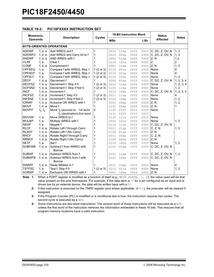
PIC18F2450/4450
DS39760D-page 216 © 2008 Microchip Technology Inc.
TABLE 19-2: PIC18FXXXX INSTRUCTION SET
Mnemonic,Operands Description Cycles
16-Bit Instruction Word StatusAffected Notes
MSb LSb
BYTE-ORIENTED OPERATIONSADDWFADDWFCANDWFCLRFCOMFCPFSEQCPFSGTCPFSLTDECFDECFSZDCFSNZINCFINCFSZINFSNZIORWFMOVFMOVFF
MOVWFMULWFNEGFRLCFRLNCFRRCFRRNCFSETFSUBFWB
SUBWFSUBWFB
SWAPFTSTFSZXORWF
f, d, af, d, af, d, af, af, d, af, af, af, af, d, af, d, af, d, af, d, af, d, af, d, af, d, af, d, afs, fd
f, af, af, af, d, af, d, af, d, af, d, af, af, d, a
f, d, af, d, a
f, d, af, af, d, a
Add WREG and fAdd WREG and Carry bit to fAND WREG with fClear fComplement fCompare f with WREG, Skip =Compare f with WREG, Skip >Compare f with WREG, Skip <Decrement fDecrement f, Skip if 0Decrement f, Skip if Not 0Increment fIncrement f, Skip if 0Increment f, Skip if Not 0Inclusive OR WREG with fMove fMove fs (source) to 1st word
fd (destination) 2nd wordMove WREG to fMultiply WREG with fNegate fRotate Left f through CarryRotate Left f (No Carry)Rotate Right f through CarryRotate Right f (No Carry)Set fSubtract f from WREG with Borrow Subtract WREG from fSubtract WREG from f with BorrowSwap Nibbles in fTest f, Skip if 0Exclusive OR WREG with f
111111 (2 or 3)1 (2 or 3)1 (2 or 3)11 (2 or 3)1 (2 or 3)11 (2 or 3)1 (2 or 3)112
111111111
11
11 (2 or 3)1
001000100001011000010110011001100000001001000010001101000001010111001111011000000110001101000011010001100101
01010101
001101100001
01da00da01da101a11da001a010a000a01da11da11da10da11da10da00da00daffffffff111a001a110a01da01da00da00da100a01da
11da10da
10da011a10da
ffffffffffffffffffffffffffffffffffffffffffffffffffffffffffffffffffffffffffffffffffffffffffffffffffffffffffff
ffffffff
ffffffffffff
ffffffffffffffffffffffffffffffffffffffffffffffffffffffffffffffffffffffffffffffffffffffffffffffffffffffffffff
ffffffff
ffffffffffff
C, DC, Z, OV, NC, DC, Z, OV, NZ, NZZ, NNoneNoneNoneC, DC, Z, OV, NNoneNoneC, DC, Z, OV, NNoneNoneZ, NZ, NNone
NoneNoneC, DC, Z, OV, NC, Z, NZ, NC, Z, NZ, NNoneC, DC, Z, OV, N
C, DC, Z, OV, NC, DC, Z, OV, N
NoneNoneZ, N
1, 21, 21,221, 2441, 21, 2, 3, 41, 2, 3, 41, 21, 2, 3, 441, 21, 21
1, 2
1, 2
1, 2
1, 2
41, 2
Note 1: When a PORT register is modified as a function of itself (e.g., MOVF PORTB, 1, 0), the value used will be that value present on the pins themselves. For example, if the data latch is �1� for a pin configured as an input and is driven low by an external device, the data will be written back with a �0�.
2: If this instruction is executed on the TMR0 register (and where applicable, �d� = 1), the prescaler will be cleared if assigned.
3: If the Program Counter (PC) is modified or a conditional test is true, the instruction requires two cycles. The second cycle is executed as a NOP.
4: Some instructions are two-word instructions. The second word of these instructions will be executed as a NOP unless the first word of the instruction retrieves the information embedded in these 16 bits. This ensures that all program memory locations have a valid instruction.
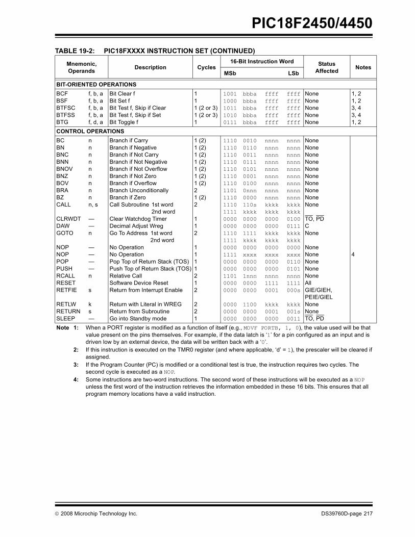
PIC18F2450/4450
© 2008 Microchip Technology Inc. DS39760D-page 217
BIT-ORIENTED OPERATIONSBCFBSFBTFSCBTFSSBTG
f, b, af, b, af, b, af, b, af, d, a
Bit Clear fBit Set fBit Test f, Skip if ClearBit Test f, Skip if SetBit Toggle f
111 (2 or 3)1 (2 or 3)1
10011000101110100111
bbbabbbabbbabbbabbba
ffffffffffffffffffff
ffffffffffffffffffff
NoneNoneNoneNoneNone
1, 21, 23, 43, 41, 2
CONTROL OPERATIONSBCBNBNCBNNBNOVBNZBOVBRABZCALL
CLRWDTDAWGOTO
NOPNOPPOPPUSHRCALLRESETRETFIE
RETLWRETURNSLEEP
nnnnnnnnnn, s
��n
����n
s
ks�
Branch if CarryBranch if NegativeBranch if Not CarryBranch if Not NegativeBranch if Not OverflowBranch if Not ZeroBranch if OverflowBranch Unconditionally Branch if ZeroCall Subroutine 1st word
2nd wordClear Watchdog TimerDecimal Adjust WregGo To Address 1st word
2nd wordNo OperationNo OperationPop Top of Return Stack (TOS)Push Top of Return Stack (TOS)Relative CallSoftware Device ResetReturn from Interrupt Enable
Return with Literal in WREG Return from SubroutineGo into Standby mode
1 (2)1 (2)1 (2)1 (2)1 (2)1 (2)1 (2)21 (2)2
112
1111212
221
1110111011101110111011101110110111101110111100000000111011110000111100000000110100000000
000000000000
00100110001101110101000101000nnn0000110skkkk000000001111kkkk0000xxxx000000001nnn00000000
110000000000
nnnnnnnnnnnnnnnnnnnnnnnnnnnnnnnnnnnnkkkkkkkk00000000kkkkkkkk0000xxxx00000000nnnn11110001
kkkk00010000
nnnnnnnnnnnnnnnnnnnnnnnnnnnnnnnnnnnnkkkkkkkk01000111kkkkkkkk0000xxxx01100101nnnn1111000s
kkkk001s0011
NoneNoneNoneNoneNoneNoneNoneNoneNoneNone
TO, PDCNone
NoneNoneNoneNoneNoneAllGIE/GIEH, PEIE/GIELNoneNoneTO, PD
4
TABLE 19-2: PIC18FXXXX INSTRUCTION SET (CONTINUED)
Mnemonic,Operands Description Cycles
16-Bit Instruction Word StatusAffected Notes
MSb LSb
Note 1: When a PORT register is modified as a function of itself (e.g., MOVF PORTB, 1, 0), the value used will be that value present on the pins themselves. For example, if the data latch is �1� for a pin configured as an input and is driven low by an external device, the data will be written back with a �0�.
2: If this instruction is executed on the TMR0 register (and where applicable, �d� = 1), the prescaler will be cleared if assigned.
3: If the Program Counter (PC) is modified or a conditional test is true, the instruction requires two cycles. The second cycle is executed as a NOP.
4: Some instructions are two-word instructions. The second word of these instructions will be executed as a NOP unless the first word of the instruction retrieves the information embedded in these 16 bits. This ensures that all program memory locations have a valid instruction.

PIC18F2450/4450
DS39760D-page 218 © 2008 Microchip Technology Inc.
LITERAL OPERATIONSADDLWANDLWIORLWLFSR
MOVLBMOVLWMULLWRETLWSUBLWXORLW
kkkf, k
kkkkkk
Add Literal and WREGAND Literal with WREGInclusive OR Literal with WREGMove Literal (12-bit) 2nd word to FSR(f) 1st wordMove Literal to BSR<3:0>Move Literal to WREGMultiply Literal with WREGReturn with Literal in WREG Subtract WREG from LiteralExclusive OR Literal with WREG
1112
111211
00000000000011101111000000000000000000000000
11111011100111100000000111101101110010001010
kkkkkkkkkkkk00ffkkkk0000kkkkkkkkkkkkkkkkkkkk
kkkkkkkkkkkkkkkkkkkkkkkkkkkkkkkkkkkkkkkkkkkk
C, DC, Z, OV, NZ, NZ, NNone
NoneNoneNoneNoneC, DC, Z, OV, NZ, N
DATA MEMORY ↔ PROGRAM MEMORY OPERATIONSTBLRD*TBLRD*+TBLRD*-TBLRD+*TBLWT*TBLWT*+TBLWT*-TBLWT+*
Table ReadTable Read with Post-IncrementTable Read with Post-DecrementTable Read with Pre-IncrementTable WriteTable Write with Post-IncrementTable Write with Post-DecrementTable Write with Pre-Increment
2
2
00000000000000000000000000000000
00000000000000000000000000000000
00000000000000000000000000000000
10001001101010111100110111101111
NoneNoneNoneNoneNoneNoneNoneNone
TABLE 19-2: PIC18FXXXX INSTRUCTION SET (CONTINUED)
Mnemonic,Operands Description Cycles
16-Bit Instruction Word StatusAffected Notes
MSb LSb
Note 1: When a PORT register is modified as a function of itself (e.g., MOVF PORTB, 1, 0), the value used will be that value present on the pins themselves. For example, if the data latch is �1� for a pin configured as an input and is driven low by an external device, the data will be written back with a �0�.
2: If this instruction is executed on the TMR0 register (and where applicable, �d� = 1), the prescaler will be cleared if assigned.
3: If the Program Counter (PC) is modified or a conditional test is true, the instruction requires two cycles. The second cycle is executed as a NOP.
4: Some instructions are two-word instructions. The second word of these instructions will be executed as a NOP unless the first word of the instruction retrieves the information embedded in these 16 bits. This ensures that all program memory locations have a valid instruction.
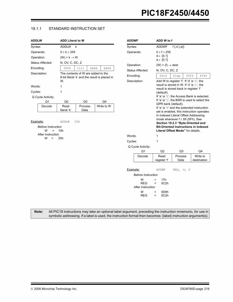
PIC18F2450/4450
© 2008 Microchip Technology Inc. DS39760D-page 219
19.1.1 STANDARD INSTRUCTION SET
ADDLW ADD Literal to W
Syntax: ADDLW k
Operands: 0 ≤ k ≤ 255
Operation: (W) + k → W
Status Affected: N, OV, C, DC, Z
Encoding: 0000 1111 kkkk kkkk
Description: The contents of W are added to the 8-bit literal �k� and the result is placed in W.
Words: 1
Cycles: 1
Q Cycle Activity:Q1 Q2 Q3 Q4
Decode Readliteral �k�
Process Data
Write to W
Example: ADDLW 15h
Before InstructionW = 10h
After InstructionW = 25h
ADDWF ADD W to f
Syntax: ADDWF f {,d {,a}}
Operands: 0 ≤ f ≤ 255d ∈ [0,1]a ∈ [0,1]
Operation: (W) + (f) → dest
Status Affected: N, OV, C, DC, Z
Encoding: 0010 01da ffff ffff
Description: Add W to register �f�. If �d� is �0�, the result is stored in W. If �d� is �1�, the result is stored back in register �f� (default). If �a� is �0�, the Access Bank is selected. If �a� is �1�, the BSR is used to select the GPR bank (default). If �a� is �0� and the extended instruction set is enabled, this instruction operates in Indexed Literal Offset Addressing mode whenever f ≤ 95 (5Fh). See Section 19.2.3 �Byte-Oriented and Bit-Oriented Instructions in Indexed Literal Offset Mode� for details.
Words: 1
Cycles: 1
Q Cycle Activity:Q1 Q2 Q3 Q4
Decode Readregister �f�
Process Data
Write todestination
Example: ADDWF REG, 0, 0
Before InstructionW = 17hREG = 0C2h
After InstructionW = 0D9hREG = 0C2h
Note: All PIC18 instructions may take an optional label argument, preceding the instruction mnemonic, for use insymbolic addressing. If a label is used, the instruction format then becomes: {label} instruction argument(s).

PIC18F2450/4450
DS39760D-page 220 © 2008 Microchip Technology Inc.
ADDWFC ADD W and Carry bit to f
Syntax: ADDWFC f {,d {,a}}
Operands: 0 ≤ f ≤ 255d ∈ [0,1]a ∈ [0,1]
Operation: (W) + (f) + (C) → dest
Status Affected: N, OV, C, DC, Z
Encoding: 0010 00da ffff ffff
Description: Add W, the Carry flag and data memory location �f�. If �d� is �0�, the result is placed in W. If �d� is �1�, the result is placed in data memory location �f�. If �a� is �0�, the Access Bank is selected. If �a� is �1�, the BSR is used to select the GPR bank (default). If �a� is �0� and the extended instruction set is enabled, this instruction operates in Indexed Literal Offset Addressing mode whenever f ≤ 95 (5Fh). See Section 19.2.3 �Byte-Oriented and Bit-Oriented Instructions in Indexed Literal Offset Mode� for details.
Words: 1
Cycles: 1
Q Cycle Activity:Q1 Q2 Q3 Q4
Decode Readregister �f�
Process Data
Write to destination
Example: ADDWFC REG, 0, 1
Before InstructionCarry bit = 1REG = 02hW = 4Dh
After InstructionCarry bit = 0REG = 02hW = 50h
ANDLW AND Literal with W
Syntax: ANDLW k
Operands: 0 ≤ k ≤ 255
Operation: (W) .AND. k → W
Status Affected: N, Z
Encoding: 0000 1011 kkkk kkkk
Description: The contents of W are ANDed with the 8-bit literal �k�. The result is placed in W.
Words: 1
Cycles: 1
Q Cycle Activity:Q1 Q2 Q3 Q4
Decode Read literal �k�
Process Data
Write to W
Example: ANDLW 05Fh
Before InstructionW = A3h
After InstructionW = 03h

PIC18F2450/4450
© 2008 Microchip Technology Inc. DS39760D-page 221
ANDWF AND W with f
Syntax: ANDWF f {,d {,a}}
Operands: 0 ≤ f ≤ 255d ∈ [0,1]a ∈ [0,1]
Operation: (W) .AND. (f) → dest
Status Affected: N, Z
Encoding: 0001 01da ffff ffff
Description: The contents of W are ANDed with register �f�. If �d� is �0�, the result is stored in W. If �d� is �1�, the result is stored back in register �f� (default). If �a� is �0�, the Access Bank is selected. If �a� is �1�, the BSR is used to select the GPR bank (default). If �a� is �0� and the extended instruction set is enabled, this instruction operates in Indexed Literal Offset Addressing mode whenever f ≤ 95 (5Fh). See Section 19.2.3 �Byte-Oriented and Bit-Oriented Instructions in Indexed Literal Offset Mode� for details.
Words: 1
Cycles: 1
Q Cycle Activity:Q1 Q2 Q3 Q4
Decode Readregister �f�
Process Data
Write to destination
Example: ANDWF REG, 0, 0
Before InstructionW = 17hREG = C2h
After InstructionW = 02hREG = C2h
BC Branch if Carry
Syntax: BC n
Operands: -128 ≤ n ≤ 127
Operation: if Carry bit is �1�,(PC) + 2 + 2n → PC
Status Affected: None
Encoding: 1110 0010 nnnn nnnn
Description: If the Carry bit is �1�, then the program will branch.The 2�s complement number �2n� is added to the PC. Since the PC will have incremented to fetch the next instruction, the new address will be PC + 2 + 2n. This instruction is then a two-cycle instruction.
Words: 1
Cycles: 1(2)
Q Cycle Activity:If Jump:
Q1 Q2 Q3 Q4Decode Read literal
�n�Process
DataWrite to PC
No operation
No operation
No operation
No operation
If No Jump:Q1 Q2 Q3 Q4
Decode Read literal �n�
Process Data
No operation
Example: HERE BC 5
Before InstructionPC = address (HERE)
After InstructionIf Carry = 1;
PC = address (HERE + 12)If Carry = 0;
PC = address (HERE + 2)
PIC18F2450/4450
DS39760D-page 222 © 2008 Microchip Technology Inc.
BCF Bit Clear f
Syntax: BCF f, b {,a}
Operands: 0 ≤ f ≤ 2550 ≤ b ≤ 7a ∈ [0,1]
Operation: 0 → f<b>
Status Affected: None
Encoding: 1001 bbba ffff ffff
Description: Bit �b� in register �f� is cleared.If �a� is �0�, the Access Bank is selected. If �a� is �1�, the BSR is used to select the GPR bank (default). If �a� is �0� and the extended instruction set is enabled, this instruction operates in Indexed Literal Offset Addressing mode whenever f ≤ 95 (5Fh). See Section 19.2.3 �Byte-Oriented and Bit-Oriented Instructions in Indexed Literal Offset Mode� for details.
Words: 1
Cycles: 1
Q Cycle Activity:Q1 Q2 Q3 Q4
Decode Readregister �f�
Process Data
Writeregister �f�
Example: BCF FLAG_REG, 7, 0
Before InstructionFLAG_REG = C7h
After InstructionFLAG_REG = 47h
BN Branch if Negative
Syntax: BN n
Operands: -128 ≤ n ≤ 127
Operation: if Negative bit is �1�,(PC) + 2 + 2n → PC
Status Affected: None
Encoding: 1110 0110 nnnn nnnn
Description: If the Negative bit is �1�, then the program will branch.The 2�s complement number �2n� is added to the PC. Since the PC will have incremented to fetch the next instruction, the new address will be PC + 2 + 2n. This instruction is then a two-cycle instruction.
Words: 1
Cycles: 1(2)
Q Cycle Activity:If Jump:
Q1 Q2 Q3 Q4Decode Read literal
�n�Process
DataWrite to PC
No operation
No operation
No operation
No operation
If No Jump:Q1 Q2 Q3 Q4
Decode Read literal �n�
Process Data
No operation
Example: HERE BN Jump
Before InstructionPC = address (HERE)
After InstructionIf Negative = 1;
PC = address (Jump)If Negative = 0;
PC = address (HERE + 2)
PIC18F2450/4450
© 2008 Microchip Technology Inc. DS39760D-page 223
BNC Branch if Not Carry
Syntax: BNC n
Operands: -128 ≤ n ≤ 127
Operation: if Carry bit is �0�,(PC) + 2 + 2n → PC
Status Affected: None
Encoding: 1110 0011 nnnn nnnn
Description: If the Carry bit is �0�, then the program will branch.The 2�s complement number �2n� is added to the PC. Since the PC will have incremented to fetch the next instruction, the new address will be PC + 2 + 2n. This instruction is then a two-cycle instruction.
Words: 1
Cycles: 1(2)
Q Cycle Activity:If Jump:
Q1 Q2 Q3 Q4Decode Read literal
�n�Process
DataWrite to PC
No operation
No operation
No operation
No operation
If No Jump:Q1 Q2 Q3 Q4
Decode Read literal �n�
Process Data
No operation
Example: HERE BNC Jump
Before InstructionPC = address (HERE)
After InstructionIf Carry = 0;
PC = address (Jump)If Carry = 1;
PC = address (HERE + 2)
BNN Branch if Not Negative
Syntax: BNN n
Operands: -128 ≤ n ≤ 127
Operation: if Negative bit is �0�,(PC) + 2 + 2n → PC
Status Affected: None
Encoding: 1110 0111 nnnn nnnn
Description: If the Negative bit is �0�, then the program will branch.The 2�s complement number �2n� is added to the PC. Since the PC will have incremented to fetch the next instruction, the new address will be PC + 2 + 2n. This instruction is then a two-cycle instruction.
Words: 1
Cycles: 1(2)
Q Cycle Activity:If Jump:
Q1 Q2 Q3 Q4Decode Read literal
�n�Process
DataWrite to PC
No operation
No operation
No operation
No operation
If No Jump:Q1 Q2 Q3 Q4
Decode Read literal �n�
Process Data
No operation
Example: HERE BNN Jump
Before InstructionPC = address (HERE)
After InstructionIf Negative = 0;
PC = address (Jump)If Negative = 1;
PC = address (HERE + 2)
PIC18F2450/4450
DS39760D-page 224 © 2008 Microchip Technology Inc.
BNOV Branch if Not Overflow
Syntax: BNOV n
Operands: -128 ≤ n ≤ 127
Operation: if Overflow bit is �0�,(PC) + 2 + 2n → PC
Status Affected: None
Encoding: 1110 0101 nnnn nnnn
Description: If the Overflow bit is �0�, then the program will branch.The 2�s complement number �2n� is added to the PC. Since the PC will have incremented to fetch the next instruction, the new address will be PC + 2 + 2n. This instruction is then a two-cycle instruction.
Words: 1
Cycles: 1(2)
Q Cycle Activity:If Jump:
Q1 Q2 Q3 Q4Decode Read literal
�n�Process
DataWrite to PC
No operation
No operation
No operation
No operation
If No Jump:Q1 Q2 Q3 Q4
Decode Read literal �n�
Process Data
No operation
Example: HERE BNOV Jump
Before InstructionPC = address (HERE)
After InstructionIf Overflow = 0;
PC = address (Jump)If Overflow = 1;
PC = address (HERE + 2)
BNZ Branch if Not Zero
Syntax: BNZ n
Operands: -128 ≤ n ≤ 127
Operation: if Zero bit is �0�,(PC) + 2 + 2n → PC
Status Affected: None
Encoding: 1110 0001 nnnn nnnn
Description: If the Zero bit is �0�, then the program will branch.The 2�s complement number �2n� is added to the PC. Since the PC will have incremented to fetch the next instruction, the new address will be PC + 2 + 2n. This instruction is then a two-cycle instruction.
Words: 1
Cycles: 1(2)
Q Cycle Activity:If Jump:
Q1 Q2 Q3 Q4Decode Read literal
�n�Process
DataWrite to PC
No operation
No operation
No operation
No operation
If No Jump:Q1 Q2 Q3 Q4
Decode Read literal �n�
Process Data
No operation
Example: HERE BNZ Jump
Before InstructionPC = address (HERE)
After InstructionIf Zero = 0;
PC = address (Jump)If Zero = 1;
PC = address (HERE + 2)
PIC18F2450/4450
© 2008 Microchip Technology Inc. DS39760D-page 225
BRA Unconditional Branch
Syntax: BRA n
Operands: -1024 ≤ n ≤ 1023
Operation: (PC) + 2 + 2n → PC
Status Affected: None
Encoding: 1101 0nnn nnnn nnnn
Description: Add the 2�s complement number �2n� to the PC. Since the PC will have incremented to fetch the next instruction, the new address will be PC + 2 + 2n. This instruction is a two-cycle instruction.
Words: 1
Cycles: 2
Q Cycle Activity:Q1 Q2 Q3 Q4
Decode Read literal �n�
Process Data
Write to PC
No operation
No operation
No operation
No operation
Example: HERE BRA Jump
Before InstructionPC = address (HERE)
After InstructionPC = address (Jump)
BSF Bit Set f
Syntax: BSF f, b {,a}
Operands: 0 ≤ f ≤ 2550 ≤ b ≤ 7a ∈ [0,1]
Operation: 1 → f<b>
Status Affected: None
Encoding: 1000 bbba ffff ffff
Description: Bit �b� in register �f� is set. If �a� is �0�, the Access Bank is selected. If �a� is �1�, the BSR is used to select the GPR bank (default). If �a� is �0� and the extended instruction set is enabled, this instruction operates in Indexed Literal Offset Addressing mode whenever f ≤ 95 (5Fh). See Section 19.2.3 �Byte-Oriented and Bit-Oriented Instructions in Indexed Literal Offset Mode� for details.
Words: 1
Cycles: 1
Q Cycle Activity:Q1 Q2 Q3 Q4
Decode Readregister �f�
Process Data
Writeregister �f�
Example: BSF FLAG_REG, 7, 1
Before InstructionFLAG_REG = 0Ah
After InstructionFLAG_REG = 8Ah

PIC18F2450/4450
DS39760D-page 226 © 2008 Microchip Technology Inc.
BTFSC Bit Test File, Skip if Clear
Syntax: BTFSC f, b {,a}
Operands: 0 ≤ f ≤ 2550 ≤ b ≤ 7a ∈ [0,1]
Operation: skip if (f<b>) = 0
Status Affected: None
Encoding: 1011 bbba ffff ffff
Description: If bit �b� in register �f� is �0�, then the next instruction is skipped. If bit �b� is �0�, then the next instruction fetched during the current instruction execution is discarded and a NOP is executed instead, making this a two-cycle instruction. If �a� is �0�, the Access Bank is selected. If �a� is �1�, the BSR is used to select the GPR bank (default). If �a� is �0� and the extended instruction set is enabled, this instruction operates in Indexed Literal Offset Addressing mode whenever f ≤ 95 (5Fh). See Section 19.2.3 �Byte-Oriented and Bit-Oriented Instructions in Indexed Literal Offset Mode� for details.
Words: 1
Cycles: 1(2)Note: 3 cycles if skip and followed
by a 2-word instruction.
Q Cycle Activity:Q1 Q2 Q3 Q4
Decode Readregister �f�
Process Data
No operation
If skip:Q1 Q2 Q3 Q4No
operationNo
operationNo
operationNo
operationIf skip and followed by 2-word instruction:
Q1 Q2 Q3 Q4No
operationNo
operationNo
operationNo
operationNo
operationNo
operationNo
operationNo
operation
Example: HEREFALSETRUE
BTFSC::
FLAG, 1, 0
Before InstructionPC = address (HERE)
After InstructionIf FLAG<1> = 0;
PC = address (TRUE)If FLAG<1> = 1;
PC = address (FALSE)
BTFSS Bit Test File, Skip if Set
Syntax: BTFSS f, b {,a}
Operands: 0 ≤ f ≤ 2550 ≤ b < 7a ∈ [0,1]
Operation: skip if (f<b>) = 1
Status Affected: None
Encoding: 1010 bbba ffff ffff
Description: If bit �b� in register �f� is �1�, then the next instruction is skipped. If bit �b� is �1�, then the next instruction fetched during the current instruction execution is discarded and a NOP is executed instead, making this a two-cycle instruction. If �a� is �0�, the Access Bank is selected. If �a� is �1�, the BSR is used to select the GPR bank (default). If �a� is �0� and the extended instruction set is enabled, this instruction operates in Indexed Literal Offset Addressing mode whenever f ≤ 95 (5Fh). See Section 19.2.3 �Byte-Oriented and Bit-Oriented Instructions in Indexed Literal Offset Mode� for details.
Words: 1
Cycles: 1(2)Note: 3 cycles if skip and followed
by a 2-word instruction.
Q Cycle Activity:Q1 Q2 Q3 Q4
Decode Readregister �f�
Process Data
No operation
If skip:Q1 Q2 Q3 Q4No
operationNo
operationNo
operationNo
operationIf skip and followed by 2-word instruction:
Q1 Q2 Q3 Q4No
operationNo
operationNo
operationNo
operationNo
operationNo
operationNo
operationNo
operation
Example: HEREFALSETRUE
BTFSS::
FLAG, 1, 0
Before InstructionPC = address (HERE)
After InstructionIf FLAG<1> = 0;
PC = address (FALSE)If FLAG<1> = 1;
PC = address (TRUE)

PIC18F2450/4450
© 2008 Microchip Technology Inc. DS39760D-page 227
BTG Bit Toggle f
Syntax: BTG f, b {,a}
Operands: 0 ≤ f ≤ 2550 ≤ b < 7a ∈ [0,1]
Operation: (f<b>) → f<b>
Status Affected: None
Encoding: 0111 bbba ffff ffff
Description: Bit �b� in data memory location �f� is inverted.If �a� is �0�, the Access Bank is selected. If �a� is �1�, the BSR is used to select the GPR bank (default). If �a� is �0� and the extended instruction set is enabled, this instruction operates in Indexed Literal Offset Addressing mode whenever f ≤ 95 (5Fh). See Section 19.2.3 �Byte-Oriented and Bit-Oriented Instructions in Indexed Literal Offset Mode� for details.
Words: 1
Cycles: 1
Q Cycle Activity:Q1 Q2 Q3 Q4
Decode Readregister �f�
Process Data
Writeregister �f�
Example: BTG PORTC, 4, 0
Before Instruction:PORTC = 0111 0101 [75h]
After Instruction:PORTC = 0110 0101 [65h]
BOV Branch if Overflow
Syntax: BOV n
Operands: -128 ≤ n ≤ 127
Operation: if Overflow bit is �1�,(PC) + 2 + 2n → PC
Status Affected: None
Encoding: 1110 0100 nnnn nnnn
Description: If the Overflow bit is �1�, then the program will branch.The 2�s complement number �2n� is added to the PC. Since the PC will have incremented to fetch the next instruction, the new address will be PC + 2 + 2n. This instruction is then a two-cycle instruction.
Words: 1
Cycles: 1(2)
Q Cycle Activity:If Jump:
Q1 Q2 Q3 Q4Decode Read literal
�n�Process
DataWrite to PC
No operation
No operation
No operation
No operation
If No Jump:Q1 Q2 Q3 Q4
Decode Read literal �n�
Process Data
No operation
Example: HERE BOV Jump
Before InstructionPC = address (HERE)
After InstructionIf Overflow = 1;
PC = address (Jump)If Overflow = 0;
PC = address (HERE + 2)
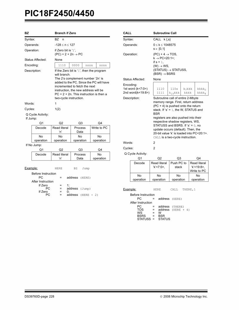
PIC18F2450/4450
DS39760D-page 228 © 2008 Microchip Technology Inc.
BZ Branch if Zero
Syntax: BZ n
Operands: -128 ≤ n ≤ 127
Operation: if Zero bit is �1�,(PC) + 2 + 2n → PC
Status Affected: None
Encoding: 1110 0000 nnnn nnnn
Description: If the Zero bit is �1�, then the program will branch.The 2�s complement number �2n� is added to the PC. Since the PC will have incremented to fetch the next instruction, the new address will be PC + 2 + 2n. This instruction is then a two-cycle instruction.
Words: 1
Cycles: 1(2)
Q Cycle Activity:If Jump:
Q1 Q2 Q3 Q4Decode Read literal
�n�Process
DataWrite to PC
No operation
No operation
No operation
No operation
If No Jump:Q1 Q2 Q3 Q4
Decode Read literal �n�
Process Data
No operation
Example: HERE BZ Jump
Before InstructionPC = address (HERE)
After InstructionIf Zero = 1;
PC = address (Jump)If Zero = 0;
PC = address (HERE + 2)
CALL Subroutine Call
Syntax: CALL k {,s}
Operands: 0 ≤ k ≤ 1048575s ∈ [0,1]
Operation: (PC) + 4 → TOS,k → PC<20:1>;if s = 1,(W) → WS,(STATUS) → STATUSS,(BSR) → BSRS
Status Affected: None
Encoding:1st word (k<7:0>)2nd word(k<19:8>)
11101111
110sk19kkk
k7kkkkkkk
kkkk0kkkk8
Description: Subroutine call of entire 2-Mbyte memory range. First, return address (PC + 4) is pushed onto the return stack. If �s� = 1, the W, STATUS and BSR registers are also pushed into their respective shadow registers, WS, STATUSS and BSRS. If �s� = 0, no update occurs (default). Then, the 20-bit value �k� is loaded into PC<20:1>. CALL is a two-cycle instruction.
Words: 2
Cycles: 2
Q Cycle Activity:Q1 Q2 Q3 Q4
Decode Read literal �k�<7:0>,
Push PC to stack
Read literal �k�<19:8>,
Write to PCNo
operationNo
operationNo
operationNo
operation
Example: HERE CALL THERE,1
Before InstructionPC = address (HERE)
After InstructionPC = address (THERE)TOS = address (HERE + 4)WS = WBSRS = BSRSTATUSS = STATUS
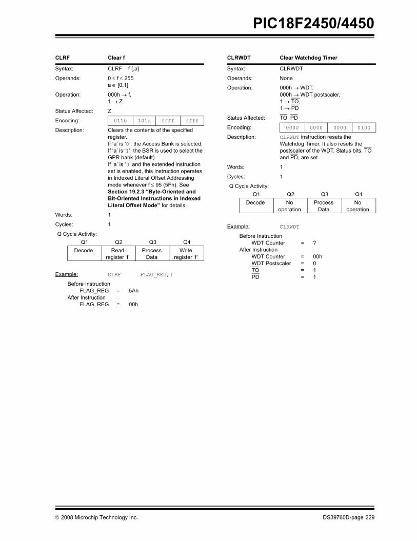
PIC18F2450/4450
© 2008 Microchip Technology Inc. DS39760D-page 229
CLRF Clear f
Syntax: CLRF f {,a}
Operands: 0 ≤ f ≤ 255a ∈ [0,1]
Operation: 000h → f,1 → Z
Status Affected: Z
Encoding: 0110 101a ffff ffff
Description: Clears the contents of the specified register. If �a� is �0�, the Access Bank is selected. If �a� is �1�, the BSR is used to select the GPR bank (default). If �a� is �0� and the extended instruction set is enabled, this instruction operates in Indexed Literal Offset Addressing mode whenever f ≤ 95 (5Fh). See Section 19.2.3 �Byte-Oriented and Bit-Oriented Instructions in Indexed Literal Offset Mode� for details.
Words: 1
Cycles: 1
Q Cycle Activity:Q1 Q2 Q3 Q4
Decode Readregister �f�
Process Data
Writeregister �f�
Example: CLRF FLAG_REG,1
Before InstructionFLAG_REG = 5Ah
After InstructionFLAG_REG = 00h
CLRWDT Clear Watchdog Timer
Syntax: CLRWDT
Operands: None
Operation: 000h → WDT,000h → WDT postscaler,1 → TO,1 → PD
Status Affected: TO, PD
Encoding: 0000 0000 0000 0100
Description: CLRWDT instruction resets the Watchdog Timer. It also resets the postscaler of the WDT. Status bits, TO and PD, are set.
Words: 1
Cycles: 1
Q Cycle Activity:Q1 Q2 Q3 Q4
Decode No operation
Process Data
No operation
Example: CLRWDT
Before InstructionWDT Counter = ?
After InstructionWDT Counter = 00hWDT Postscaler = 0TO = 1PD = 1
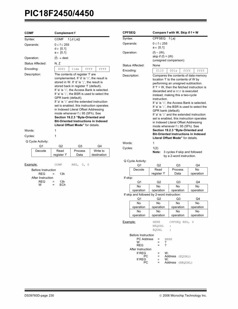
PIC18F2450/4450
DS39760D-page 230 © 2008 Microchip Technology Inc.
COMF Complement f
Syntax: COMF f {,d {,a}}
Operands: 0 ≤ f ≤ 255d ∈ [0,1]a ∈ [0,1]
Operation: (f) → dest
Status Affected: N, Z
Encoding: 0001 11da ffff ffff
Description: The contents of register �f� are complemented. If �d� is �0�, the result is stored in W. If �d� is �1�, the result is stored back in register �f� (default). If �a� is �0�, the Access Bank is selected. If �a� is �1�, the BSR is used to select the GPR bank (default). If �a� is �0� and the extended instruction set is enabled, this instruction operates in Indexed Literal Offset Addressing mode whenever f ≤ 95 (5Fh). See Section 19.2.3 �Byte-Oriented and Bit-Oriented Instructions in Indexed Literal Offset Mode� for details.
Words: 1
Cycles: 1
Q Cycle Activity:Q1 Q2 Q3 Q4
Decode Readregister �f�
Process Data
Write todestination
Example: COMF REG, 0, 0
Before InstructionREG = 13h
After InstructionREG = 13hW = ECh
CPFSEQ Compare f with W, Skip if f = W
Syntax: CPFSEQ f {,a}Operands: 0 ≤ f ≤ 255
a ∈ [0,1]Operation: (f) � (W),
skip if (f) = (W) (unsigned comparison)
Status Affected: NoneEncoding: 0110 001a ffff ffff
Description: Compares the contents of data memory location �f� to the contents of W by performing an unsigned subtraction.If �f� = W, then the fetched instruction is discarded and a NOP is executed instead, making this a two-cycle instruction. If �a� is �0�, the Access Bank is selected. If �a� is �1�, the BSR is used to select the GPR bank (default). If �a� is �0� and the extended instruction set is enabled, this instruction operates in Indexed Literal Offset Addressing mode whenever f ≤ 95 (5Fh). See Section 19.2.3 �Byte-Oriented and Bit-Oriented Instructions in Indexed Literal Offset Mode� for details.
Words: 1Cycles: 1(2)
Note: 3 cycles if skip and followedby a 2-word instruction.
Q Cycle Activity:Q1 Q2 Q3 Q4
Decode Readregister �f�
Process Data
No operation
If skip:Q1 Q2 Q3 Q4No
operationNo
operationNo
operationNo
operationIf skip and followed by 2-word instruction:
Q1 Q2 Q3 Q4No
operationNo
operationNo
operationNo
operationNo
operationNo
operationNo
operationNo
operation
Example: HERE CPFSEQ REG, 0NEQUAL :EQUAL :
Before InstructionPC Address = HEREW = ?REG = ?
After InstructionIf REG = W;
PC = Address (EQUAL)If REG ≠ W;
PC = Address (NEQUAL)
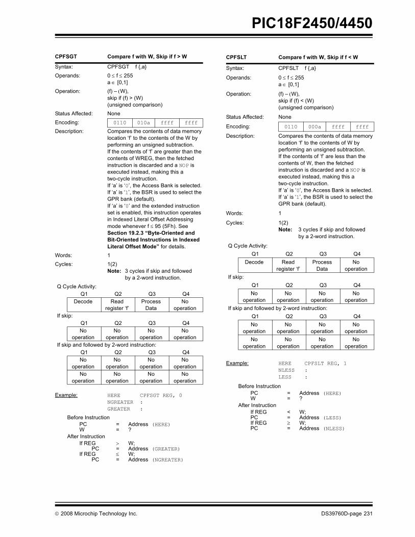
PIC18F2450/4450
© 2008 Microchip Technology Inc. DS39760D-page 231
CPFSGT Compare f with W, Skip if f > W
Syntax: CPFSGT f {,a}Operands: 0 ≤ f ≤ 255
a ∈ [0,1]Operation: (f) � (W),
skip if (f) > (W) (unsigned comparison)
Status Affected: NoneEncoding: 0110 010a ffff ffff
Description: Compares the contents of data memory location �f� to the contents of the W by performing an unsigned subtraction.If the contents of �f� are greater than the contents of WREG, then the fetched instruction is discarded and a NOP is executed instead, making this a two-cycle instruction. If �a� is �0�, the Access Bank is selected. If �a� is �1�, the BSR is used to select the GPR bank (default). If �a� is �0� and the extended instruction set is enabled, this instruction operates in Indexed Literal Offset Addressing mode whenever f ≤ 95 (5Fh). See Section 19.2.3 �Byte-Oriented and Bit-Oriented Instructions in Indexed Literal Offset Mode� for details.
Words: 1Cycles: 1(2)
Note: 3 cycles if skip and followedby a 2-word instruction.
Q Cycle Activity:Q1 Q2 Q3 Q4
Decode Readregister �f�
Process Data
No operation
If skip:Q1 Q2 Q3 Q4No
operationNo
operationNo
operationNo
operationIf skip and followed by 2-word instruction:
Q1 Q2 Q3 Q4No
operationNo
operationNo
operationNo
operationNo
operationNo
operationNo
operationNo
operation
Example: HERE CPFSGT REG, 0NGREATER :GREATER :
Before InstructionPC = Address (HERE)W = ?
After InstructionIf REG > W;
PC = Address (GREATER)If REG ≤ W;
PC = Address (NGREATER)
CPFSLT Compare f with W, Skip if f < W
Syntax: CPFSLT f {,a}
Operands: 0 ≤ f ≤ 255a ∈ [0,1]
Operation: (f) � (W),skip if (f) < (W) (unsigned comparison)
Status Affected: None
Encoding: 0110 000a ffff ffff
Description: Compares the contents of data memory location �f� to the contents of W by performing an unsigned subtraction.If the contents of �f� are less than the contents of W, then the fetched instruction is discarded and a NOP is executed instead, making this a two-cycle instruction. If �a� is �0�, the Access Bank is selected. If �a� is �1�, the BSR is used to select the GPR bank (default).
Words: 1
Cycles: 1(2)Note: 3 cycles if skip and followed
by a 2-word instruction.
Q Cycle Activity:Q1 Q2 Q3 Q4
Decode Readregister �f�
Process Data
No operation
If skip:Q1 Q2 Q3 Q4No
operationNo
operationNo
operationNo
operationIf skip and followed by 2-word instruction:
Q1 Q2 Q3 Q4No
operationNo
operationNo
operationNo
operationNo
operationNo
operationNo
operationNo
operation
Example: HERE CPFSLT REG, 1NLESS :LESS :
Before InstructionPC = Address (HERE)W = ?
After InstructionIf REG < W;PC = Address (LESS)If REG ≥ W;PC = Address (NLESS)
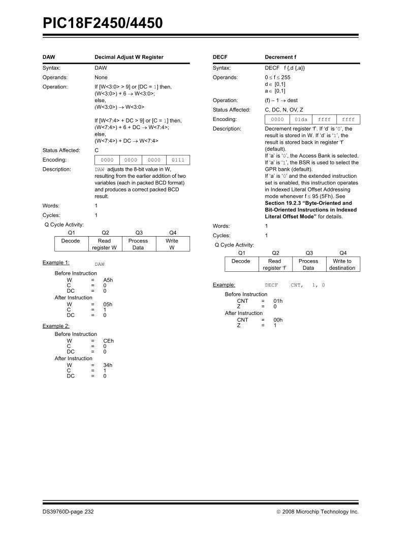
PIC18F2450/4450
DS39760D-page 232 © 2008 Microchip Technology Inc.
DAW Decimal Adjust W Register
Syntax: DAW
Operands: None
Operation: If [W<3:0> > 9] or [DC = 1] then,(W<3:0>) + 6 → W<3:0>;else, (W<3:0>) → W<3:0>
If [W<7:4> + DC > 9] or [C = 1] then,(W<7:4>) + 6 + DC → W<7:4>;else, (W<7:4>) + DC → W<7:4>
Status Affected: C
Encoding: 0000 0000 0000 0111
Description: DAW adjusts the 8-bit value in W, resulting from the earlier addition of two variables (each in packed BCD format) and produces a correct packed BCD result.
Words: 1
Cycles: 1
Q Cycle Activity:Q1 Q2 Q3 Q4
Decode Readregister W
Process Data
WriteW
Example 1: DAW
Before InstructionW = A5hC = 0DC = 0
After InstructionW = 05hC = 1DC = 0
Example 2:Before Instruction
W = CEhC = 0DC = 0
After InstructionW = 34hC = 1DC = 0
DECF Decrement f
Syntax: DECF f {,d {,a}}
Operands: 0 ≤ f ≤ 255d ∈ [0,1]a ∈ [0,1]
Operation: (f) � 1 → dest
Status Affected: C, DC, N, OV, Z
Encoding: 0000 01da ffff ffff
Description: Decrement register �f�. If �d� is �0�, the result is stored in W. If �d� is �1�, the result is stored back in register �f� (default). If �a� is �0�, the Access Bank is selected. If �a� is �1�, the BSR is used to select the GPR bank (default). If �a� is �0� and the extended instruction set is enabled, this instruction operates in Indexed Literal Offset Addressing mode whenever f ≤ 95 (5Fh). See Section 19.2.3 �Byte-Oriented and Bit-Oriented Instructions in Indexed Literal Offset Mode� for details.
Words: 1
Cycles: 1
Q Cycle Activity:Q1 Q2 Q3 Q4
Decode Readregister �f�
Process Data
Write to destination
Example: DECF CNT, 1, 0
Before InstructionCNT = 01hZ = 0
After InstructionCNT = 00hZ = 1

PIC18F2450/4450
© 2008 Microchip Technology Inc. DS39760D-page 233
DECFSZ Decrement f, Skip if 0
Syntax: DECFSZ f {,d {,a}}
Operands: 0 ≤ f ≤ 255d ∈ [0,1]a ∈ [0,1]
Operation: (f) � 1 → dest,skip if result = 0
Status Affected: None
Encoding: 0010 11da ffff ffff
Description: The contents of register �f� are decremented. If �d� is �0�, the result is placed in W. If �d� is �1�, the result is placed back in register �f� (default).If the result is �0�, the next instruction, which is already fetched, is discarded and a NOP is executed instead, making it a two-cycle instruction.If �a� is �0�, the Access Bank is selected. If �a� is �1�, the BSR is used to select the GPR bank (default). If �a� is �0� and the extended instruction set is enabled, this instruction operates in Indexed Literal Offset Addressing mode whenever f ≤ 95 (5Fh). See Section 19.2.3 �Byte-Oriented and Bit-Oriented Instructions in Indexed Literal Offset Mode� for details.
Words: 1
Cycles: 1(2)Note: 3 cycles if skip and followed
by a 2-word instruction.
Q Cycle Activity:Q1 Q2 Q3 Q4
Decode Readregister �f�
Process Data
Write to destination
If skip:Q1 Q2 Q3 Q4No
operationNo
operationNo
operationNo
operationIf skip and followed by 2-word instruction:
Q1 Q2 Q3 Q4No
operationNo
operationNo
operationNo
operationNo
operationNo
operationNo
operationNo
operation
Example: HERE DECFSZ CNT, 1, 1 GOTO LOOPCONTINUE
Before InstructionPC = Address (HERE)
After InstructionCNT = CNT � 1If CNT = 0;
PC = Address (CONTINUE)If CNT ≠ 0;
PC = Address (HERE + 2)
DCFSNZ Decrement f, Skip if Not 0
Syntax: DCFSNZ f {,d {,a}}
Operands: 0 ≤ f ≤ 255d ∈ [0,1]a ∈ [0,1]
Operation: (f) � 1 → dest,skip if result ≠ 0
Status Affected: None
Encoding: 0100 11da ffff ffff
Description: The contents of register �f� are decremented. If �d� is �0�, the result is placed in W. If �d� is �1�, the result is placed back in register �f� (default).If the result is not �0�, the next instruction, which is already fetched, is discarded and a NOP is executed instead, making it a two-cycle instruction. If �a� is �0�, the Access Bank is selected. If �a� is �1�, the BSR is used to select the GPR bank (default). If �a� is �0� and the extended instruction set is enabled, this instruction operates in Indexed Literal Offset Addressing mode whenever f ≤ 95 (5Fh). See Section 19.2.3 �Byte-Oriented and Bit-Oriented Instructions in Indexed Literal Offset Mode� for details.
Words: 1
Cycles: 1(2)Note: 3 cycles if skip and followed
by a 2-word instruction.
Q Cycle Activity:Q1 Q2 Q3 Q4
Decode Readregister �f�
Process Data
Write to destination
If skip:Q1 Q2 Q3 Q4No
operationNo
operationNo
operationNo
operationIf skip and followed by 2-word instruction:
Q1 Q2 Q3 Q4No
operationNo
operationNo
operationNo
operationNo
operationNo
operationNo
operationNo
operation
Example: HERE DCFSNZ TEMP, 1, 0ZERO : NZERO :
Before InstructionTEMP = ?
After InstructionTEMP = TEMP � 1,If TEMP = 0;
PC = Address (ZERO)If TEMP ≠ 0;
PC = Address (NZERO)
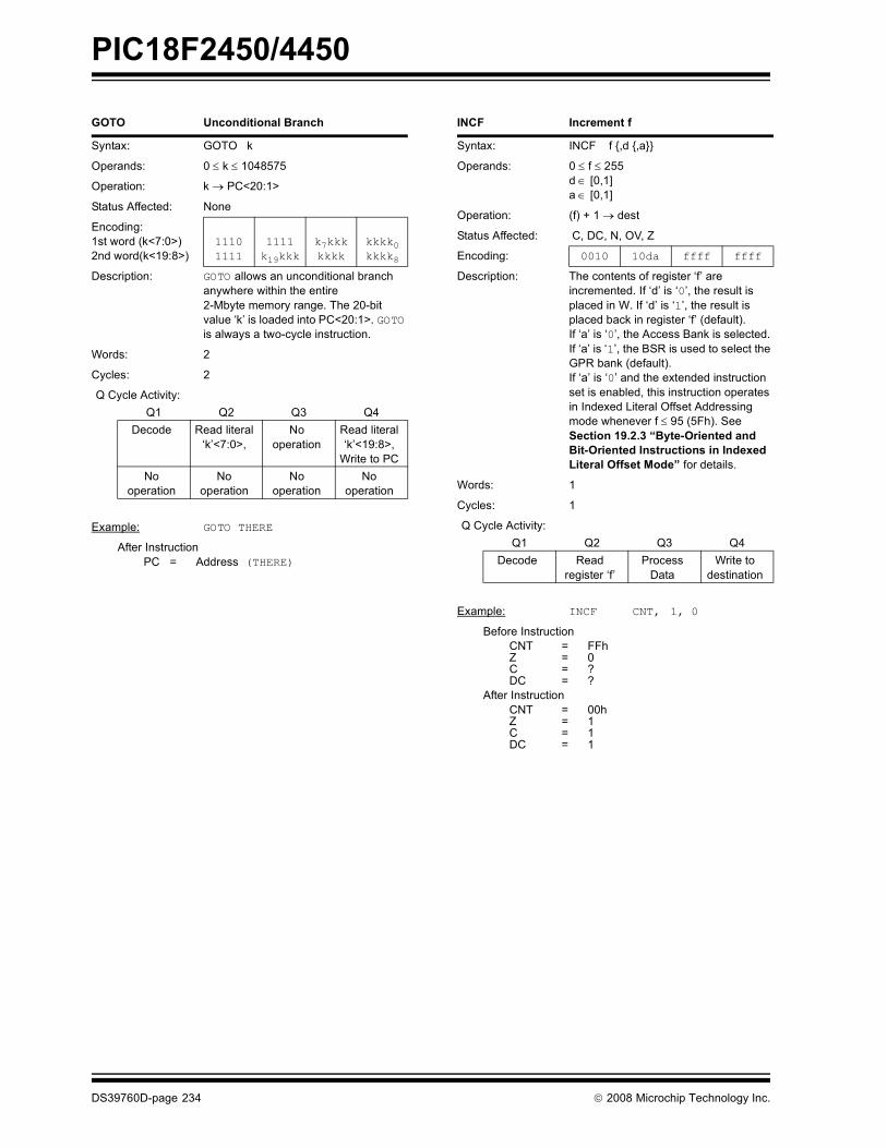
PIC18F2450/4450
DS39760D-page 234 © 2008 Microchip Technology Inc.
GOTO Unconditional Branch
Syntax: GOTO k
Operands: 0 ≤ k ≤ 1048575
Operation: k → PC<20:1>
Status Affected: None
Encoding:1st word (k<7:0>)2nd word(k<19:8>)
11101111
1111k19kkk
k7kkkkkkk
kkkk0kkkk8
Description: GOTO allows an unconditional branch anywhere within the entire 2-Mbyte memory range. The 20-bit value �k� is loaded into PC<20:1>. GOTO is always a two-cycle instruction.
Words: 2
Cycles: 2
Q Cycle Activity:Q1 Q2 Q3 Q4
Decode Read literal �k�<7:0>,
No operation
Read literal �k�<19:8>,
Write to PCNo
operationNo
operationNo
operationNo
operation
Example: GOTO THERE
After InstructionPC = Address (THERE)
INCF Increment f
Syntax: INCF f {,d {,a}}
Operands: 0 ≤ f ≤ 255d ∈ [0,1]a ∈ [0,1]
Operation: (f) + 1 → dest
Status Affected: C, DC, N, OV, Z
Encoding: 0010 10da ffff ffff
Description: The contents of register �f� are incremented. If �d� is �0�, the result is placed in W. If �d� is �1�, the result is placed back in register �f� (default). If �a� is �0�, the Access Bank is selected. If �a� is �1�, the BSR is used to select the GPR bank (default). If �a� is �0� and the extended instruction set is enabled, this instruction operates in Indexed Literal Offset Addressing mode whenever f ≤ 95 (5Fh). See Section 19.2.3 �Byte-Oriented and Bit-Oriented Instructions in Indexed Literal Offset Mode� for details.
Words: 1
Cycles: 1
Q Cycle Activity:Q1 Q2 Q3 Q4
Decode Readregister �f�
Process Data
Write to destination
Example: INCF CNT, 1, 0
Before InstructionCNT = FFhZ = 0C = ?DC = ?
After InstructionCNT = 00hZ = 1C = 1DC = 1

PIC18F2450/4450
© 2008 Microchip Technology Inc. DS39760D-page 235
INCFSZ Increment f, Skip if 0
Syntax: INCFSZ f {,d {,a}}
Operands: 0 ≤ f ≤ 255d ∈ [0,1]a ∈ [0,1]
Operation: (f) + 1 → dest,skip if result = 0
Status Affected: None
Encoding: 0011 11da ffff ffff
Description: The contents of register �f� are incremented. If �d� is �0�, the result is placed in W. If �d� is �1�, the result is placed back in register �f�. (default)If the result is �0�, the next instruction, which is already fetched, is discarded and a NOP is executed instead, making it a two-cycle instruction. If �a� is �0�, the Access Bank is selected. If �a� is �1�, the BSR is used to select the GPR bank (default). If �a� is �0� and the extended instruction set is enabled, this instruction operates in Indexed Literal Offset Addressing mode whenever f ≤ 95 (5Fh). See Section 19.2.3 �Byte-Oriented and Bit-Oriented Instructions in Indexed Literal Offset Mode� for details.
Words: 1
Cycles: 1(2)Note: 3 cycles if skip and followed
by a 2-word instruction.
Q Cycle Activity:Q1 Q2 Q3 Q4
Decode Readregister �f�
Process Data
Write to destination
If skip:Q1 Q2 Q3 Q4No
operationNo
operationNo
operationNo
operationIf skip and followed by 2-word instruction:
Q1 Q2 Q3 Q4No
operationNo
operationNo
operationNo
operationNo
operationNo
operationNo
operationNo
operation
Example: HERE INCFSZ CNT, 1, 0NZERO : ZERO :
Before InstructionPC = Address (HERE)
After InstructionCNT = CNT + 1If CNT = 0;PC = Address (ZERO)If CNT ≠ 0;PC = Address (NZERO)
INFSNZ Increment f, Skip if Not 0
Syntax: INFSNZ f {,d {,a}}Operands: 0 ≤ f ≤ 255
d ∈ [0,1]a ∈ [0,1]
Operation: (f) + 1 → dest, skip if result ≠ 0
Status Affected: NoneEncoding: 0100 10da ffff ffff
Description: The contents of register �f� are incremented. If �d� is �0�, the result is placed in W. If �d� is �1�, the result is placed back in register �f� (default).If the result is not �0�, the next instruction, which is already fetched, is discarded and a NOP is executed instead, making it a two-cycle instruction. If �a� is �0�, the Access Bank is selected. If �a� is �1�, the BSR is used to select the GPR bank (default). If �a� is �0� and the extended instruction set is enabled, this instruction operates in Indexed Literal Offset Addressing mode whenever f ≤ 95 (5Fh). See Section 19.2.3 �Byte-Oriented and Bit-Oriented Instructions in Indexed Literal Offset Mode� for details.
Words: 1Cycles: 1(2)
Note: 3 cycles if skip and followedby a 2-word instruction.
Q Cycle Activity:Q1 Q2 Q3 Q4
Decode Readregister �f�
Process Data
Write to destination
If skip:Q1 Q2 Q3 Q4No
operationNo
operationNo
operationNo
operationIf skip and followed by 2-word instruction:
Q1 Q2 Q3 Q4No
operationNo
operationNo
operationNo
operationNo
operationNo
operationNo
operationNo
operation
Example: HERE INFSNZ REG, 1, 0ZERONZERO
Before InstructionPC = Address (HERE)
After InstructionREG = REG + 1If REG ≠ 0;PC = Address (NZERO)If REG = 0;PC = Address (ZERO)

PIC18F2450/4450
DS39760D-page 236 © 2008 Microchip Technology Inc.
IORLW Inclusive OR Literal with W
Syntax: IORLW k
Operands: 0 ≤ k ≤ 255
Operation: (W) .OR. k → W
Status Affected: N, Z
Encoding: 0000 1001 kkkk kkkk
Description: The contents of W are ORed with the 8-bit literal �k�. The result is placed in W.
Words: 1
Cycles: 1
Q Cycle Activity:Q1 Q2 Q3 Q4
Decode Read literal �k�
Process Data
Write to W
Example: IORLW 35h
Before InstructionW = 9Ah
After InstructionW = BFh
IORWF Inclusive OR W with f
Syntax: IORWF f {,d {,a}}
Operands: 0 ≤ f ≤ 255d ∈ [0,1]a ∈ [0,1]
Operation: (W) .OR. (f) → dest
Status Affected: N, Z
Encoding: 0001 00da ffff ffff
Description: Inclusive OR W with register �f�. If �d� is �0�, the result is placed in W. If �d� is �1�, the result is placed back in register �f� (default). If �a� is �0�, the Access Bank is selected. If �a� is �1�, the BSR is used to select the GPR bank (default). If �a� is �0� and the extended instruction set is enabled, this instruction operates in Indexed Literal Offset Addressing mode whenever f ≤ 95 (5Fh). See Section 19.2.3 �Byte-Oriented and Bit-Oriented Instructions in Indexed Literal Offset Mode� for details.
Words: 1
Cycles: 1
Q Cycle Activity:Q1 Q2 Q3 Q4
Decode Readregister �f�
Process Data
Write to destination
Example: IORWF RESULT, 0, 1
Before InstructionRESULT = 13hW = 91h
After InstructionRESULT = 13hW = 93h

PIC18F2450/4450
© 2008 Microchip Technology Inc. DS39760D-page 237
LFSR Load FSR
Syntax: LFSR f, k
Operands: 0 ≤ f ≤ 20 ≤ k ≤ 4095
Operation: k → FSRf
Status Affected: None
Encoding: 11101111
11100000
00ffk7kkk
k11kkkkkkk
Description: The 12-bit literal �k� is loaded into the File Select Register pointed to by �f�.
Words: 2
Cycles: 2
Q Cycle Activity:Q1 Q2 Q3 Q4
Decode Read literal �k� MSB
Process Data
Writeliteral �k� MSB
to FSRfHDecode Read literal
�k� LSBProcess
Data Write literal �k�
to FSRfL
Example: LFSR 2, 3ABh
After InstructionFSR2H = 03hFSR2L = ABh
MOVF Move f
Syntax: MOVF f {,d {,a}}
Operands: 0 ≤ f ≤ 255d ∈ [0,1]a ∈ [0,1]
Operation: f → dest
Status Affected: N, Z
Encoding: 0101 00da ffff ffff
Description: The contents of register �f� are moved to a destination dependent upon the status of �d�. If �d� is �0�, the result is placed in W. If �d� is �1�, the result is placed back in register �f� (default). Location �f� can be anywhere in the 256-byte bank.If �a� is �0�, the Access Bank is selected. If �a� is �1�, the BSR is used to select the GPR bank (default). If �a� is �0� and the extended instruction set is enabled, this instruction operates in Indexed Literal Offset Addressing mode whenever f ≤ 95 (5Fh). See Section 19.2.3 �Byte-Oriented and Bit-Oriented Instructions in Indexed Literal Offset Mode� for details.
Words: 1
Cycles: 1
Q Cycle Activity:Q1 Q2 Q3 Q4
Decode Readregister �f�
Process Data
Write W
Example: MOVF REG, 0, 0
Before InstructionREG = 22hW = FFh
After InstructionREG = 22hW = 22h
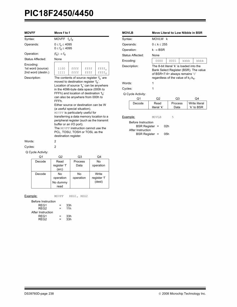
PIC18F2450/4450
DS39760D-page 238 © 2008 Microchip Technology Inc.
MOVFF Move f to f
Syntax: MOVFF fs,fdOperands: 0 ≤ fs ≤ 4095
0 ≤ fd ≤ 4095
Operation: (fs) → fdStatus Affected: None
Encoding:1st word (source)2nd word (destin.)
11001111
ffffffff
ffffffff
ffffsffffd
Description: The contents of source register �fs� are moved to destination register �fd�. Location of source �fs� can be anywhere in the 4096-byte data space (000h to FFFh) and location of destination �fd� can also be anywhere from 000h to FFFh.Either source or destination can be W (a useful special situation).MOVFF is particularly useful for transferring a data memory location to a peripheral register (such as the transmit buffer or an I/O port).The MOVFF instruction cannot use the PCL, TOSU, TOSH or TOSL as the destination register.
Words: 2
Cycles: 2
Q Cycle Activity:Q1 Q2 Q3 Q4
Decode Readregister �f�
(src)
Process Data
No operation
Decode No operation
No dummy read
No operation
Write register �f�
(dest)
Example: MOVFF REG1, REG2
Before InstructionREG1 = 33hREG2 = 11h
After InstructionREG1 = 33hREG2 = 33h
MOVLB Move Literal to Low Nibble in BSR
Syntax: MOVLW k
Operands: 0 ≤ k ≤ 255
Operation: k → BSR
Status Affected: None
Encoding: 0000 0001 kkkk kkkk
Description: The 8-bit literal �k� is loaded into the Bank Select Register (BSR). The value of BSR<7:4> always remains �0� regardless of the value of k7:k4.
Words: 1
Cycles: 1
Q Cycle Activity:Q1 Q2 Q3 Q4
Decode Readliteral �k�
Process Data
Write literal �k� to BSR
Example: MOVLB 5
Before InstructionBSR Register = 02h
After InstructionBSR Register = 05h
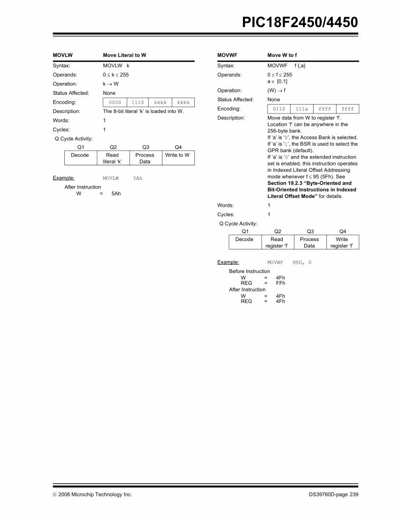
PIC18F2450/4450
© 2008 Microchip Technology Inc. DS39760D-page 239
MOVLW Move Literal to W
Syntax: MOVLW k
Operands: 0 ≤ k ≤ 255
Operation: k → W
Status Affected: None
Encoding: 0000 1110 kkkk kkkk
Description: The 8-bit literal �k� is loaded into W.
Words: 1
Cycles: 1
Q Cycle Activity:Q1 Q2 Q3 Q4
Decode Readliteral �k�
Process Data
Write to W
Example: MOVLW 5Ah
After InstructionW = 5Ah
MOVWF Move W to f
Syntax: MOVWF f {,a}
Operands: 0 ≤ f ≤ 255a ∈ [0,1]
Operation: (W) → f
Status Affected: None
Encoding: 0110 111a ffff ffff
Description: Move data from W to register �f�. Location �f� can be anywhere in the 256-byte bank. If �a� is �0�, the Access Bank is selected. If �a� is �1�, the BSR is used to select the GPR bank (default). If �a� is �0� and the extended instruction set is enabled, this instruction operates in Indexed Literal Offset Addressing mode whenever f ≤ 95 (5Fh). See Section 19.2.3 �Byte-Oriented and Bit-Oriented Instructions in Indexed Literal Offset Mode� for details.
Words: 1
Cycles: 1
Q Cycle Activity:Q1 Q2 Q3 Q4
Decode Readregister �f�
Process Data
Writeregister �f�
Example: MOVWF REG, 0
Before InstructionW = 4FhREG = FFh
After InstructionW = 4FhREG = 4Fh

PIC18F2450/4450
DS39760D-page 240 © 2008 Microchip Technology Inc.
MULLW Multiply Literal with W
Syntax: MULLW k
Operands: 0 ≤ k ≤ 255
Operation: (W) x k → PRODH:PRODL
Status Affected: None
Encoding: 0000 1101 kkkk kkkk
Description: An unsigned multiplication is carried out between the contents of W and the 8-bit literal �k�. The 16-bit result is placed in PRODH:PRODL register pair. PRODH contains the high byte.W is unchanged.None of the Status flags are affected.Note that neither Overflow nor Carry is possible in this operation. A zero result is possible but not detected.
Words: 1
Cycles: 1
Q Cycle Activity:Q1 Q2 Q3 Q4
Decode Read literal �k�
Process Data
Write registers PRODH:PRODL
Example: MULLW 0C4h
Before InstructionW = E2hPRODH = ?PRODL = ?
After InstructionW = E2hPRODH = ADhPRODL = 08h
MULWF Multiply W with f
Syntax: MULWF f {,a}
Operands: 0 ≤ f ≤ 255a ∈ [0,1]
Operation: (W) x (f) → PRODH:PRODL
Status Affected: None
Encoding: 0000 001a ffff ffff
Description: An unsigned multiplication is carried out between the contents of W and the register file location �f�. The 16-bit result is stored in the PRODH:PRODL register pair. PRODH contains the high byte. Both W and �f� are unchanged.None of the Status flags are affected.Note that neither Overflow nor Carry is possible in this operation. A zero result is possible but not detected.If �a� is �0�, the Access Bank is selected. If �a� is �1�, the BSR is used to select the GPR bank (default). If �a� is �0� and the extended instruction set is enabled, this instruction operates in Indexed Literal Offset Addressing mode whenever f ≤ 95 (5Fh). See Section 19.2.3 �Byte-Oriented and Bit-Oriented Instructions in Indexed Literal Offset Mode� for details.
Words: 1
Cycles: 1
Q Cycle Activity:Q1 Q2 Q3 Q4
Decode Readregister �f�
Process Data
Writeregisters PRODH:PRODL
Example: MULWF REG, 1
Before InstructionW = C4hREG = B5hPRODH = ?PRODL = ?
After InstructionW = C4hREG = B5hPRODH = 8AhPRODL = 94h
PIC18F2450/4450
© 2008 Microchip Technology Inc. DS39760D-page 241
NEGF Negate f
Syntax: NEGF f {,a}
Operands: 0 ≤ f ≤ 255a ∈ [0,1]
Operation: (f) + 1 → f
Status Affected: N, OV, C, DC, Z
Encoding: 0110 110a ffff ffff
Description: Location �f� is negated using two�s complement. The result is placed in the data memory location �f�. If �a� is �0�, the Access Bank is selected. If �a� is �1�, the BSR is used to select the GPR bank (default). If �a� is �0� and the extended instruction set is enabled, this instruction operates in Indexed Literal Offset Addressing mode whenever f ≤ 95 (5Fh). See Section 19.2.3 �Byte-Oriented and Bit-Oriented Instructions in Indexed Literal Offset Mode� for details.
Words: 1
Cycles: 1
Q Cycle Activity:Q1 Q2 Q3 Q4
Decode Readregister �f�
Process Data
Write register �f�
Example: NEGF REG, 1
Before InstructionREG = 0011 1010 [3Ah]
After InstructionREG = 1100 0110 [C6h]
NOP No Operation
Syntax: NOP
Operands: None
Operation: No operation
Status Affected: None
Encoding: 00001111
0000xxxx
0000xxxx
0000xxxx
Description: No operation.
Words: 1
Cycles: 1
Q Cycle Activity:Q1 Q2 Q3 Q4
Decode No operation
No operation
No operation
Example:
None.

PIC18F2450/4450
DS39760D-page 242 © 2008 Microchip Technology Inc.
POP Pop Top of Return Stack
Syntax: POP
Operands: None
Operation: (TOS) → bit bucket
Status Affected: None
Encoding: 0000 0000 0000 0110
Description: The TOS value is pulled off the return stack and is discarded. The TOS value then becomes the previous value that was pushed onto the return stack.This instruction is provided to enable the user to properly manage the return stack to incorporate a software stack.
Words: 1
Cycles: 1
Q Cycle Activity:Q1 Q2 Q3 Q4
Decode Nooperation
Pop TOS value
Nooperation
Example: POPGOTO NEW
Before InstructionTOS = 0031A2hStack (1 level down) = 014332h
After InstructionTOS = 014332hPC = NEW
PUSH Push Top of Return Stack
Syntax: PUSH
Operands: None
Operation: (PC + 2) → TOS
Status Affected: None
Encoding: 0000 0000 0000 0101
Description: The PC + 2 is pushed onto the top of the return stack. The previous TOS value is pushed down on the stack.This instruction allows implementing a software stack by modifying TOS and then pushing it onto the return stack.
Words: 1
Cycles: 1
Q Cycle Activity:Q1 Q2 Q3 Q4
Decode Push PC + 2 onto return
stack
No operation
No operation
Example: PUSH
Before InstructionTOS = 345AhPC = 0124h
After InstructionPC = 0126hTOS = 0126hStack (1 level down) = 345Ah

PIC18F2450/4450
© 2008 Microchip Technology Inc. DS39760D-page 243
RCALL Relative Call
Syntax: RCALL n
Operands: -1024 ≤ n ≤ 1023
Operation: (PC) + 2 → TOS,(PC) + 2 + 2n → PC
Status Affected: None
Encoding: 1101 1nnn nnnn nnnn
Description: Subroutine call with a jump up to 1K from the current location. First, return address (PC + 2) is pushed onto the stack. Then, add the 2�s complement number �2n� to the PC. Since the PC will have incremented to fetch the next instruction, the new address will be PC + 2 + 2n. This instruction is a two-cycle instruction.
Words: 1
Cycles: 2
Q Cycle Activity:Q1 Q2 Q3 Q4
Decode Read literal �n�
Push PC to stack
Process Data
Write to PC
No operation
No operation
No operation
No operation
Example: HERE RCALL Jump
Before InstructionPC = Address (HERE)
After InstructionPC = Address (Jump)TOS = Address (HERE + 2)
RESET Reset
Syntax: RESET
Operands: None
Operation: Reset all registers and flags that are affected by a MCLR Reset.
Status Affected: All
Encoding: 0000 0000 1111 1111
Description: This instruction provides a way to execute a MCLR Reset in software.
Words: 1
Cycles: 1
Q Cycle Activity:Q1 Q2 Q3 Q4
Decode Start Reset
No operation
No operation
Example: RESET
After InstructionRegisters = Reset ValueFlags* = Reset Value

PIC18F2450/4450
DS39760D-page 244 © 2008 Microchip Technology Inc.
RETFIE Return from Interrupt
Syntax: RETFIE {s}
Operands: s ∈ [0,1]
Operation: (TOS) → PC,1 → GIE/GIEH or PEIE/GIEL;if s = 1,(WS) → W,(STATUSS) → STATUS,(BSRS) → BSR,PCLATU, PCLATH are unchanged
Status Affected: GIE/GIEH, PEIE/GIEL.
Encoding: 0000 0000 0001 000s
Description: Return from interrupt. Stack is popped and Top-of-Stack (TOS) is loaded into the PC. Interrupts are enabled by setting either the high or low-priority global interrupt enable bit. If �s� = 1, the contents of the shadow registers WS, STATUSS and BSRS are loaded into their corresponding registers, W, STATUS and BSR. If �s� = 0, no update of these registers occurs (default).
Words: 1
Cycles: 2
Q Cycle Activity:Q1 Q2 Q3 Q4
Decode No operation
No operation
Pop PC from stack
Set GIEH or GIEL
No operation
No operation
No operation
No operation
Example: RETFIE 1
After InterruptPC = TOSW = WSBSR = BSRSSTATUS = STATUSSGIE/GIEH, PEIE/GIEL = 1
RETLW Return Literal to W
Syntax: RETLW k
Operands: 0 ≤ k ≤ 255
Operation: k → W,(TOS) → PC,PCLATU, PCLATH are unchanged
Status Affected: None
Encoding: 0000 1100 kkkk kkkk
Description: W is loaded with the 8-bit literal �k�. The program counter is loaded from the top of the stack (the return address). The high address latch (PCLATH) remains unchanged.
Words: 1
Cycles: 2
Q Cycle Activity:Q1 Q2 Q3 Q4
Decode Readliteral �k�
Process Data
Pop PC from stack, Write
to WNo
operationNo
operationNo
operationNo
operation
Example:
CALL TABLE ; W contains table ; offset value ; W now has ; table value :TABLE
ADDWF PCL ; W = offsetRETLW k0 ; Begin tableRETLW k1 ;
: :
RETLW kn ; End of table
Before InstructionW = 07h
After InstructionW = value of kn
PIC18F2450/4450
© 2008 Microchip Technology Inc. DS39760D-page 245
RETURN Return from Subroutine
Syntax: RETURN {s}
Operands: s ∈ [0,1]
Operation: (TOS) → PC;if s = 1,(WS) → W,(STATUSS) → STATUS,(BSRS) → BSR,PCLATU, PCLATH are unchanged
Status Affected: None
Encoding: 0000 0000 0001 001s
Description: Return from subroutine. The stack is popped and the top of the stack (TOS) is loaded into the program counter. If �s�= 1, the contents of the shadow registers WS, STATUSS and BSRS are loaded into their corresponding registers, W, STATUS and BSR. If �s� = 0, no update of these registers occurs (default).
Words: 1
Cycles: 2
Q Cycle Activity:Q1 Q2 Q3 Q4
Decode No operation
Process Data
Pop PC from stack
No operation
No operation
No operation
No operation
Example: RETURN
After Instruction:PC = TOS
RLCF Rotate Left f through Carry
Syntax: RLCF f {,d {,a}}
Operands: 0 ≤ f ≤ 255d ∈ [0,1]a ∈ [0,1]
Operation: (f<n>) → dest<n + 1>,(f<7>) → C,(C) → dest<0>
Status Affected: C, N, Z
Encoding: 0011 01da ffff ffff
Description: The contents of register �f� are rotated one bit to the left through the Carry flag. If �d� is �0�, the result is placed in W. If �d� is �1�, the result is stored back in register �f� (default). If �a� is �0�, the Access Bank is selected. If �a� is �1�, the BSR is used to select the GPR bank (default). If �a� is �0� and the extended instruction set is enabled, this instruction operates in Indexed Literal Offset Addressing mode whenever f ≤ 95 (5Fh). See Section 19.2.3 �Byte-Oriented and Bit-Oriented Instructions in Indexed Literal Offset Mode� for details.
Words: 1
Cycles: 1
Q Cycle Activity:Q1 Q2 Q3 Q4
Decode Readregister �f�
Process Data
Write to destination
Example: RLCF REG, 0, 0
Before InstructionREG = 1110 0110C = 0
After InstructionREG = 1110 0110W = 1100 1100C = 1
C register f
PIC18F2450/4450
DS39760D-page 246 © 2008 Microchip Technology Inc.
RLNCF Rotate Left f (No Carry)
Syntax: RLNCF f {,d {,a}}
Operands: 0 ≤ f ≤ 255d ∈ [0,1]a ∈ [0,1]
Operation: (f<n>) → dest<n + 1>,(f<7>) → dest<0>
Status Affected: N, Z
Encoding: 0100 01da ffff ffff
Description: The contents of register �f� are rotated one bit to the left. If �d� is �0�, the result is placed in W. If �d� is �1�, the result is stored back in register �f� (default).If �a� is �0�, the Access Bank is selected. If �a� is �1�, the BSR is used to select the GPR bank (default). If �a� is �0� and the extended instruction set is enabled, this instruction operates in Indexed Literal Offset Addressing mode whenever f ≤ 95 (5Fh). See Section 19.2.3 �Byte-Oriented and Bit-Oriented Instructions in Indexed Literal Offset Mode� for details.
Words: 1
Cycles: 1
Q Cycle Activity:Q1 Q2 Q3 Q4
Decode Readregister �f�
Process Data
Write to destination
Example: RLNCF REG, 1, 0
Before InstructionREG = 1010 1011
After InstructionREG = 0101 0111
register f
RRCF Rotate Right f through Carry
Syntax: RRCF f {,d {,a}}
Operands: 0 ≤ f ≤ 255d ∈ [0,1]a ∈ [0,1]
Operation: (f<n>) → dest<n � 1>,(f<0>) → C,(C) → dest<7>
Status Affected: C, N, Z
Encoding: 0011 00da ffff ffff
Description: The contents of register �f� are rotated one bit to the right through the Carry flag. If �d� is �0�, the result is placed in W. If �d� is �1�, the result is placed back in register �f� (default). If �a� is �0�, the Access Bank is selected. If �a� is �1�, the BSR is used to select the GPR bank (default). If �a� is �0� and the extended instruction set is enabled, this instruction operates in Indexed Literal Offset Addressing mode whenever f ≤ 95 (5Fh). See Section 19.2.3 �Byte-Oriented and Bit-Oriented Instructions in Indexed Literal Offset Mode� for details.
Words: 1
Cycles: 1
Q Cycle Activity:Q1 Q2 Q3 Q4
Decode Readregister �f�
Process Data
Write to destination
Example: RRCF REG, 0, 0
Before InstructionREG = 1110 0110C = 0
After InstructionREG = 1110 0110W = 0111 0011C = 0
C register f

PIC18F2450/4450
© 2008 Microchip Technology Inc. DS39760D-page 247
RRNCF Rotate Right f (No Carry)
Syntax: RRNCF f {,d {,a}}
Operands: 0 ≤ f ≤ 255d ∈ [0,1]a ∈ [0,1]
Operation: (f<n>) → dest<n � 1>,(f<0>) → dest<7>
Status Affected: N, Z
Encoding: 0100 00da ffff ffff
Description: The contents of register �f� are rotated one bit to the right. If �d� is �0�, the result is placed in W. If �d� is �1�, the result is placed back in register �f� (default).If �a� is �0�, the Access Bank will be selected, overriding the BSR value. If �a� is �1�, then the bank will be selected as per the BSR value (default).If �a� is �0� and the extended instruction set is enabled, this instruction operates in Indexed Literal Offset Addressing mode whenever f ≤ 95 (5Fh). See Section 19.2.3 �Byte-Oriented and Bit-Oriented Instructions in Indexed Literal Offset Mode� for details.
Words: 1
Cycles: 1
Q Cycle Activity:Q1 Q2 Q3 Q4
Decode Readregister �f�
Process Data
Write to destination
Example 1: RRNCF REG, 1, 0
Before InstructionREG = 1101 0111
After InstructionREG = 1110 1011
Example 2: RRNCF REG, 0, 0
Before InstructionW = ?REG = 1101 0111
After InstructionW = 1110 1011REG = 1101 0111
register f
SETF Set f
Syntax: SETF f {,a}
Operands: 0 ≤ f ≤ 255a ∈ [0,1]
Operation: FFh → f
Status Affected: None
Encoding: 0110 100a ffff ffff
Description: The contents of the specified register are set to FFh. If �a� is �0�, the Access Bank is selected. If �a� is �1�, the BSR is used to select the GPR bank (default). If �a� is �0� and the extended instruction set is enabled, this instruction operates in Indexed Literal Offset Addressing mode whenever f ≤ 95 (5Fh). See Section 19.2.3 �Byte-Oriented and Bit-Oriented Instructions in Indexed Literal Offset Mode� for details.
Words: 1
Cycles: 1
Q Cycle Activity:Q1 Q2 Q3 Q4
Decode Readregister �f�
Process Data
Writeregister �f�
Example: SETF REG,1
Before InstructionREG = 5Ah
After InstructionREG = FFh

PIC18F2450/4450
DS39760D-page 248 © 2008 Microchip Technology Inc.
SLEEP Enter Sleep Mode
Syntax: SLEEP
Operands: None
Operation: 00h → WDT,0 → WDT postscaler,1 → TO,0 → PD
Status Affected: TO, PD
Encoding: 0000 0000 0000 0011
Description: The Power-Down status bit (PD) is cleared. The Time-out status bit (TO) is set. Watchdog Timer and its postscaler are cleared.The processor is put into Sleep mode with the oscillator stopped.
Words: 1
Cycles: 1
Q Cycle Activity:Q1 Q2 Q3 Q4
Decode No operation
Process Data
Go toSleep
Example: SLEEP
Before InstructionTO = ?PD = ?
After InstructionTO = 1 �PD = 0
� If WDT causes wake-up, this bit is cleared.
SUBFWB Subtract f from W with Borrow
Syntax: SUBFWB f {,d {,a}}
Operands: 0 ≤ f ≤ 255d ∈ [0,1]a ∈ [0,1]
Operation: (W) � (f) � (C) → dest
Status Affected: N, OV, C, DC, Z
Encoding: 0101 01da ffff ffff
Description: Subtract register �f� and Carry flag (borrow) from W (2�s complement method). If �d� is �0�, the result is stored in W. If �d� is �1�, the result is stored in register �f� (default). If �a� is �0�, the Access Bank is selected. If �a� is �1�, the BSR is used to select the GPR bank (default). If �a� is �0� and the extended instruction set is enabled, this instruction operates in Indexed Literal Offset Addressing mode whenever f ≤ 95 (5Fh). See Section 19.2.3 �Byte-Oriented and Bit-Oriented Instructions in Indexed Literal Offset Mode� for details.
Words: 1
Cycles: 1
Q Cycle Activity:Q1 Q2 Q3 Q4
Decode Readregister �f�
Process Data
Write to destination
Example 1: SUBFWB REG, 1, 0
Before InstructionREG = 3W = 2C = 1
After InstructionREG = FFW = 2C = 0Z = 0N = 1 ; result is negative
Example 2: SUBFWB REG, 0, 0
Before InstructionREG = 2W = 5C = 1
After InstructionREG = 2W = 3C = 1Z = 0N = 0 ; result is positive
Example 3: SUBFWB REG, 1, 0
Before InstructionREG = 1W = 2C = 0
After InstructionREG = 0W = 2C = 1Z = 1 ; result is zeroN = 0
PIC18F2450/4450
© 2008 Microchip Technology Inc. DS39760D-page 249
SUBLW Subtract W from Literal
Syntax: SUBLW k
Operands: 0 ≤ k ≤ 255
Operation: k � (W) → W
Status Affected: N, OV, C, DC, Z
Encoding: 0000 1000 kkkk kkkk
Description W is subtracted from the 8-bit literal �k�. The result is placed in W.
Words: 1
Cycles: 1
Q Cycle Activity:Q1 Q2 Q3 Q4
Decode Readliteral �k�
Process Data
Write to W
Example 1: SUBLW 02h
Before InstructionW = 01hC = ?
After InstructionW = 01hC = 1 ; result is positiveZ = 0N = 0
Example 2: SUBLW 02h
Before InstructionW = 02hC = ?
After InstructionW = 00hC = 1 ; result is zeroZ = 1N = 0
Example 3: SUBLW 02h
Before InstructionW = 03hC = ?
After InstructionW = FFh ; (2�s complement)C = 0 ; result is negativeZ = 0N = 1
SUBWF Subtract W from f
Syntax: SUBWF f {,d {,a}}
Operands: 0 ≤ f ≤ 255d ∈ [0,1]a ∈ [0,1]
Operation: (f) � (W) → dest
Status Affected: N, OV, C, DC, Z
Encoding: 0101 11da ffff ffff
Description: Subtract W from register �f� (2�s complement method). If �d� is �0�, the result is stored in W. If �d� is �1�, the result is stored back in register �f� (default). If �a� is �0�, the Access Bank is selected. If �a� is �1�, the BSR is used to select the GPR bank (default). If �a� is �0� and the extended instruction set is enabled, this instruction operates in Indexed Literal Offset Addressing mode whenever f ≤ 95 (5Fh). See Section 19.2.3 �Byte-Oriented and Bit-Oriented Instructions in Indexed Literal Offset Mode� for details.
Words: 1
Cycles: 1
Q Cycle Activity:Q1 Q2 Q3 Q4
Decode Readregister �f�
Process Data
Write to destination
Example 1: SUBWF REG, 1, 0
Before InstructionREG = 3W = 2C = ?
After InstructionREG = 1W = 2C = 1 ; result is positiveZ = 0N = 0
Example 2: SUBWF REG, 0, 0
Before InstructionREG = 2W = 2C = ?
After InstructionREG = 2W = 0C = 1 ; result is zeroZ = 1N = 0
Example 3: SUBWF REG, 1, 0
Before InstructionREG = 1W = 2C = ?
After InstructionREG = FFh ;(2�s complement)W = 2C = 0 ; result is negativeZ = 0N = 1
PIC18F2450/4450
DS39760D-page 250 © 2008 Microchip Technology Inc.
SUBWFB Subtract W from f with Borrow
Syntax: SUBWFB f {,d {,a}}Operands: 0 ≤ f ≤ 255
d ∈ [0,1]a ∈ [0,1]
Operation: (f) � (W) � (C) → destStatus Affected: N, OV, C, DC, ZEncoding: 0101 10da ffff ffff
Description: Subtract W and the Carry flag (borrow) from register �f� (2�s complement method). If �d� is �0�, the result is stored in W. If �d� is �1�, the result is stored back in register �f� (default).If �a� is �0�, the Access Bank is selected. If �a� is �1�, the BSR is used to select the GPR bank (default). If �a� is �0� and the extended instruction set is enabled, this instruction operates in Indexed Literal Offset Addressing mode whenever f ≤ 95 (5Fh). See Section 19.2.3 �Byte-Oriented and Bit-Oriented Instructions in Indexed Literal Offset Mode� for details.
Words: 1Cycles: 1Q Cycle Activity:
Q1 Q2 Q3 Q4Decode Read
register �f�Process
DataWrite to
destination
Example 1: SUBWFB REG, 1, 0
Before InstructionREG = 19h (0001 1001)W = 0Dh (0000 1101)C = 1
After InstructionREG = 0Ch (0000 1011)W = 0Dh (0000 1101)C = 1Z = 0N = 0 ; result is positive
Example 2: SUBWFB REG, 0, 0
Before InstructionREG = 1Bh (0001 1011)W = 1Ah (0001 1010)C = 0
After InstructionREG = 1Bh (0001 1011)W = 00hC = 1Z = 1 ; result is zeroN = 0
Example 3: SUBWFB REG, 1, 0
Before InstructionREG = 03h (0000 0011)W = 0Eh (0000 1101)C = 1
After InstructionREG = F5h (1111 0100)
; [2�s comp]W = 0Eh (0000 1101)C = 0Z = 0N = 1 ; result is negative
SWAPF Swap f
Syntax: SWAPF f {,d {,a}}
Operands: 0 ≤ f ≤ 255d ∈ [0,1]a ∈ [0,1]
Operation: (f<3:0>) → dest<7:4>,(f<7:4>) → dest<3:0>
Status Affected: None
Encoding: 0011 10da ffff ffff
Description: The upper and lower nibbles of register �f� are exchanged. If �d� is �0�, the result is placed in W. If �d� is �1�, the result is placed in register �f� (default).If �a� is �0�, the Access Bank is selected. If �a� is �1�, the BSR is used to select the GPR bank (default). If �a� is �0� and the extended instruction set is enabled, this instruction operates in Indexed Literal Offset Addressing mode whenever f ≤ 95 (5Fh). See Section 19.2.3 �Byte-Oriented and Bit-Oriented Instructions in Indexed Literal Offset Mode� for details.
Words: 1
Cycles: 1
Q Cycle Activity:Q1 Q2 Q3 Q4
Decode Readregister �f�
Process Data
Write to destination
Example: SWAPF REG, 1, 0
Before InstructionREG = 53h
After InstructionREG = 35h
PIC18F2450/4450
© 2008 Microchip Technology Inc. DS39760D-page 251
TBLRD Table Read
Syntax: TBLRD ( *; *+; *-; +*)
Operands: None
Operation: if TBLRD *,(Prog Mem (TBLPTR)) → TABLAT,TBLPTR � No Change;if TBLRD *+,(Prog Mem (TBLPTR)) → TABLAT,(TBLPTR) + 1 → TBLPTR;if TBLRD *-,(Prog Mem (TBLPTR)) → TABLAT,(TBLPTR) � 1 → TBLPTR;if TBLRD +*,(TBLPTR) + 1 → TBLPTR,(Prog Mem (TBLPTR)) → TABLAT
Status Affected: None
Encoding: 0000 0000 0000 10nn nn=0 * =1 *+ =2 *- =3 +*
Description: This instruction is used to read the contents of Program Memory (P.M.). To address the program memory, a pointer called Table Pointer (TBLPTR) is used.The TBLPTR (a 21-bit pointer) points to each byte in the program memory. TBLPTR has a 2-Mbyte address range.
TBLPTR<0> = 0: Least Significant Byte of Program Memory Word
TBLPTR<0> = 1: Most Significant Byte of Program Memory Word
The TBLRD instruction can modify the value of TBLPTR as follows:� no change� post-increment� post-decrement� pre-increment
Words: 1
Cycles: 2
Q Cycle Activity:Q1 Q2 Q3 Q4
Decode No operation
No operation
No operation
No operation
No operation(Read Program
Memory)
No operation
No operation(Write
TABLAT)
TBLRD Table Read (Continued)
Example 1: TBLRD *+ ;
Before InstructionTABLAT = 55hTBLPTR = 00A356hMEMORY (00A356h) = 34h
After InstructionTABLAT = 34hTBLPTR = 00A357h
Example 2: TBLRD +* ;
Before InstructionTABLAT = AAhTBLPTR = 01A357hMEMORY (01A357h) = 12hMEMORY (01A358h) = 34h
After InstructionTABLAT = 34hTBLPTR = 01A358h
PIC18F2450/4450
DS39760D-page 252 © 2008 Microchip Technology Inc.
TBLWT Table Write
Syntax: TBLWT ( *; *+; *-; +*)Operands: NoneOperation: if TBLWT*,
(TABLAT) → Holding Register,TBLPTR � No Change;if TBLWT*+,(TABLAT) → Holding Register,(TBLPTR) + 1 → TBLPTR;if TBLWT*-,(TABLAT) → Holding Register,(TBLPTR) � 1 → TBLPTR;if TBLWT+*,(TBLPTR) + 1 → TBLPTR,(TABLAT) → Holding Register
Status Affected: NoneEncoding: 0000 0000 0000 11nn
nn=0 * =1 *+ =2 *- =3 +*
Description: This instruction uses the 3 LSBs of TBLPTR to determine which of the 8 holding registers the TABLAT is written to. The holding registers are used to program the contents of Program Memory (P.M.). (Refer to Section 6.0 �Flash Program Memory� for additional details on programming Flash memory.)The TBLPTR (a 21-bit pointer) points to each byte in the program memory. TBLPTR has a 2-Mbyte address range. The LSb of the TBLPTR selects which byte of the program memory location to access.
TBLPTR<0> = 0: Least Significant Byte of Program Memory Word
TBLPTR<0> = 1: Most Significant Byte of Program Memory Word
The TBLWT instruction can modify the value of TBLPTR as follows:� no change� post-increment� post-decrement� pre-increment
Words: 1Cycles: 2 Q Cycle Activity:
Q1 Q2 Q3 Q4Decode No
operationNo
operationNo
operationNo
operationNo
operation(Read
TABLAT)
No operation
No operation(Write to Holding
Register)
TBLWT Table Write (Continued)
Example 1: TBLWT *+;
Before InstructionTABLAT = 55hTBLPTR = 00A356hHOLDING REGISTER (00A356h) = FFh
After Instructions (table write completion)TABLAT = 55hTBLPTR = 00A357hHOLDING REGISTER (00A356h) = 55h
Example 2: TBLWT +*;
Before InstructionTABLAT = 34hTBLPTR = 01389AhHOLDING REGISTER (01389Ah) = FFhHOLDING REGISTER (01389Bh) = FFh
After Instruction (table write completion)TABLAT = 34hTBLPTR = 01389BhHOLDING REGISTER (01389Ah) = FFhHOLDING REGISTER (01389Bh) = 34h

PIC18F2450/4450
© 2008 Microchip Technology Inc. DS39760D-page 253
TSTFSZ Test f, Skip if 0
Syntax: TSTFSZ f {,a}
Operands: 0 ≤ f ≤ 255a ∈ [0,1]
Operation: skip if f = 0
Status Affected: None
Encoding: 0110 011a ffff ffff
Description: If �f� = 0, the next instruction fetched during the current instruction execution is discarded and a NOP is executed, making this a two-cycle instruction. If �a� is �0�, the Access Bank is selected. If �a� is �1�, the BSR is used to select the GPR bank (default). If �a� is �0� and the extended instruction set is enabled, this instruction operates in Indexed Literal Offset Addressing mode whenever f ≤ 95 (5Fh). See Section 19.2.3 �Byte-Oriented and Bit-Oriented Instructions in Indexed Literal Offset Mode� for details.
Words: 1
Cycles: 1(2)Note: 3 cycles if skip and followed
by a 2-word instruction.
Q Cycle Activity:Q1 Q2 Q3 Q4
Decode Readregister �f�
Process Data
No operation
If skip:Q1 Q2 Q3 Q4No
operationNo
operationNo
operationNo
operationIf skip and followed by 2-word instruction:
Q1 Q2 Q3 Q4No
operationNo
operationNo
operationNo
operationNo
operationNo
operationNo
operationNo
operation
Example: HERE TSTFSZ CNT, 1NZERO :ZERO :
Before InstructionPC = Address (HERE)
After InstructionIf CNT = 00h,PC = Address (ZERO)If CNT ≠ 00h,PC = Address (NZERO)
XORLW Exclusive OR Literal with W
Syntax: XORLW k
Operands: 0 ≤ k ≤ 255
Operation: (W) .XOR. k → W
Status Affected: N, Z
Encoding: 0000 1010 kkkk kkkk
Description: The contents of W are XORed with the 8-bit literal �k�. The result is placed in W.
Words: 1
Cycles: 1
Q Cycle Activity:
Q1 Q2 Q3 Q4Decode Read
literal �k�Process
DataWrite to W
Example: XORLW 0AFh
Before InstructionW = B5h
After InstructionW = 1Ah
PIC18F2450/4450
DS39760D-page 254 © 2008 Microchip Technology Inc.
XORWF Exclusive OR W with f
Syntax: XORWF f {,d {,a}}
Operands: 0 ≤ f ≤ 255d ∈ [0,1]a ∈ [0,1]
Operation: (W) .XOR. (f) → dest
Status Affected: N, Z
Encoding: 0001 10da ffff ffff
Description: Exclusive OR the contents of W with register �f�. If �d� is �0�, the result is stored in W. If �d� is �1�, the result is stored back in the register �f� (default). If �a� is �0�, the Access Bank is selected. If �a� is �1�, the BSR is used to select the GPR bank (default). If �a� is �0� and the extended instruction set is enabled, this instruction operates in Indexed Literal Offset Addressing mode whenever f ≤ 95 (5Fh). See Section 19.2.3 �Byte-Oriented and Bit-Oriented Instructions in Indexed Literal Offset Mode� for details.
Words: 1
Cycles: 1
Q Cycle Activity:Q1 Q2 Q3 Q4
Decode Readregister �f�
Process Data
Write to destination
Example: XORWF REG, 1, 0
Before InstructionREG = AFhW = B5h
After InstructionREG = 1AhW = B5h
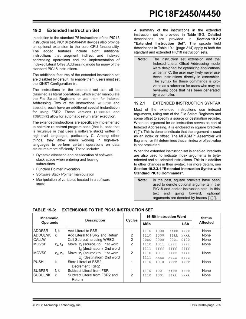
PIC18F2450/4450
© 2008 Microchip Technology Inc. DS39760D-page 255
19.2 Extended Instruction SetIn addition to the standard 75 instructions of the PIC18instruction set, PIC18F2450/4450 devices also providean optional extension to the core CPU functionality.The added features include eight additionalinstructions that augment indirect and indexedaddressing operations and the implementation ofIndexed Literal Offset Addressing mode for many of thestandard PIC18 instructions.
The additional features of the extended instruction setare disabled by default. To enable them, users must setthe XINST Configuration bit.
The instructions in the extended set can all beclassified as literal operations, which either manipulatethe File Select Registers, or use them for IndexedAddressing. Two of the instructions, ADDFSR andSUBFSR, each have an additional special instantiationfor using FSR2. These versions (ADDULNK andSUBULNK) allow for automatic return after execution.
The extended instructions are specifically implementedto optimize re-entrant program code (that is, code thatis recursive or that uses a software stack) written inhigh-level languages, particularly C. Among otherthings, they allow users working in high-levellanguages to perform certain operations on datastructures more efficiently. These include:
� Dynamic allocation and deallocation of software stack space when entering and leaving subroutines
� Function Pointer invocation� Software Stack Pointer manipulation� Manipulation of variables located in a software
stack
A summary of the instructions in the extendedinstruction set is provided in Table 19-3. Detaileddescriptions are provided in Section 19.2.2�Extended Instruction Set�. The opcode fielddescriptions in Table 19-1 (page 214) apply to both thestandard and extended PIC18 instruction sets.
19.2.1 EXTENDED INSTRUCTION SYNTAXMost of the extended instructions use indexedarguments, using one of the File Select Registers andsome offset to specify a source or destination register.When an argument for an instruction serves as part ofIndexed Addressing, it is enclosed in square brackets(�[ ]�). This is done to indicate that the argument is usedas an index or offset. The MPASM� Assembler willflag an error if it determines that an index or offset valueis not bracketed.
When the extended instruction set is enabled, bracketsare also used to indicate index arguments in byte-oriented and bit-oriented instructions. This is in additionto other changes in their syntax. For more details, seeSection 19.2.3.1 �Extended Instruction Syntax withStandard PIC18 Commands�.
TABLE 19-3: EXTENSIONS TO THE PIC18 INSTRUCTION SET
Note: The instruction set extension and theIndexed Literal Offset Addressing modewere designed for optimizing applicationswritten in C; the user may likely never usethese instructions directly in assembler.The syntax for these commands is pro-vided as a reference for users who may bereviewing code that has been generatedby a compiler.
Note: In the past, square brackets have beenused to denote optional arguments in thePIC18 and earlier instruction sets. In thistext and going forward, optionalarguments are denoted by braces (�{ }�).
Mnemonic,Operands Description Cycles
16-Bit Instruction Word StatusAffectedMSb LSb
ADDFSRADDULNKCALLWMOVSF
MOVSS
PUSHL
SUBFSRSUBULNK
f, kk
zs, fd
zs, zd
k
f, kk
Add Literal to FSRAdd Literal to FSR2 and ReturnCall Subroutine using WREGMove zs (source) to 1st word
fd (destination) 2nd wordMove zs (source) to 1st word
zd (destination) 2nd wordStore Literal at FSR2, Decrement FSR2Subtract Literal from FSRSubtract Literal from FSR2 and Return
1222
2
1
12
11101110000011101111111011111110
11101110
1000100000001011ffff1011xxxx1010
10011001
ffkk 11kk 00010zzzffff1zzzxzzzkkkk
ffkk11kk
kkkkkkkk0100zzzzffffzzzzzzzzkkkk
kkkkkkkk
NoneNoneNoneNone
None
None
NoneNone
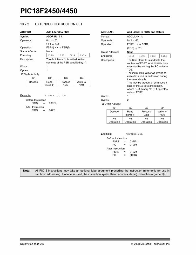
PIC18F2450/4450
DS39760D-page 256 © 2008 Microchip Technology Inc.
19.2.2 EXTENDED INSTRUCTION SET
ADDFSR Add Literal to FSR
Syntax: ADDFSR f, kOperands: 0 ≤ k ≤ 63
f ∈ [ 0, 1, 2 ]Operation: FSR(f) + k → FSR(f)Status Affected: NoneEncoding: 1110 1000 ffkk kkkk
Description: The 6-bit literal �k� is added to the contents of the FSR specified by �f�.
Words: 1Cycles: 1Q Cycle Activity:
Q1 Q2 Q3 Q4Decode Read
literal �k�Process
DataWrite to
FSR
Example: ADDFSR 2, 23h
Before InstructionFSR2 = 03FFh
After InstructionFSR2 = 0422h
ADDULNK Add Literal to FSR2 and Return
Syntax: ADDULNK kOperands: 0 ≤ k ≤ 63Operation: FSR2 + k → FSR2,
(TOS) → PCStatus Affected: NoneEncoding: 1110 1000 11kk kkkk
Description: The 6-bit literal �k� is added to the contents of FSR2. A RETURN is then executed by loading the PC with the TOS. The instruction takes two cycles to execute; a NOP is performed during the second cycle.This may be thought of as a special case of the ADDFSR instruction, where f = 3 (binary �11�); it operates only on FSR2.
Words: 1Cycles: 2Q Cycle Activity:
Q1 Q2 Q3 Q4Decode Read
literal �k�Process
DataWrite to
FSRNo
OperationNo
OperationNo
OperationNo
Operation
Example: ADDULNK 23h
Before InstructionFSR2 = 03FFhPC = 0100h
After InstructionFSR2 = 0422hPC = (TOS)
Note: All PIC18 instructions may take an optional label argument preceding the instruction mnemonic for use insymbolic addressing. If a label is used, the instruction syntax then becomes: {label} instruction argument(s).
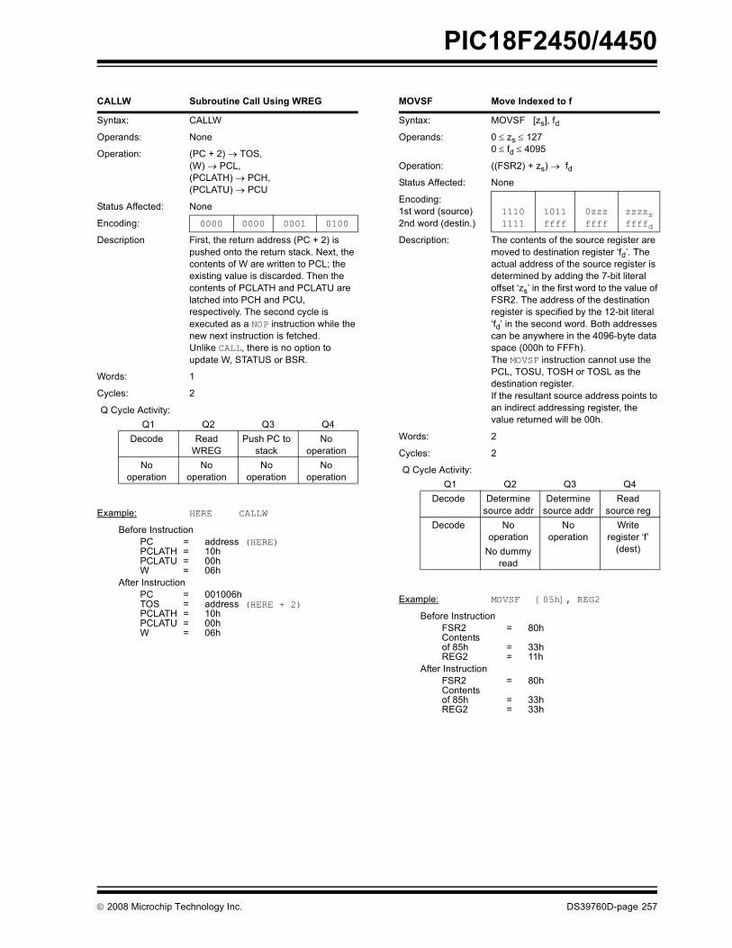
PIC18F2450/4450
© 2008 Microchip Technology Inc. DS39760D-page 257
CALLW Subroutine Call Using WREG
Syntax: CALLW
Operands: None
Operation: (PC + 2) → TOS,(W) → PCL,(PCLATH) → PCH,(PCLATU) → PCU
Status Affected: None
Encoding: 0000 0000 0001 0100
Description First, the return address (PC + 2) is pushed onto the return stack. Next, the contents of W are written to PCL; the existing value is discarded. Then the contents of PCLATH and PCLATU are latched into PCH and PCU, respectively. The second cycle is executed as a NOP instruction while the new next instruction is fetched.Unlike CALL, there is no option to update W, STATUS or BSR.
Words: 1
Cycles: 2
Q Cycle Activity:Q1 Q2 Q3 Q4
Decode Read WREG
Push PC to stack
No operation
No operation
No operation
No operation
No operation
Example: HERE CALLW
Before InstructionPC = address (HERE)PCLATH = 10hPCLATU = 00hW = 06h
After InstructionPC = 001006hTOS = address (HERE + 2)PCLATH = 10hPCLATU = 00hW = 06h
MOVSF Move Indexed to f
Syntax: MOVSF [zs], fdOperands: 0 ≤ zs ≤ 127
0 ≤ fd ≤ 4095
Operation: ((FSR2) + zs) → fdStatus Affected: None
Encoding:1st word (source)2nd word (destin.)
11101111
1011ffff
0zzzffff
zzzzsffffd
Description: The contents of the source register are moved to destination register �fd�. The actual address of the source register is determined by adding the 7-bit literal offset �zs� in the first word to the value of FSR2. The address of the destination register is specified by the 12-bit literal �fd� in the second word. Both addresses can be anywhere in the 4096-byte data space (000h to FFFh).The MOVSF instruction cannot use the PCL, TOSU, TOSH or TOSL as the destination register.If the resultant source address points to an indirect addressing register, the value returned will be 00h.
Words: 2
Cycles: 2
Q Cycle Activity:Q1 Q2 Q3 Q4
Decode Determine source addr
Determinesource addr
Read source reg
Decode No operation
No dummy read
No operation
Write register �f�
(dest)
Example: MOVSF [05h], REG2
Before InstructionFSR2 = 80hContents of 85h = 33hREG2 = 11h
After InstructionFSR2 = 80hContentsof 85h = 33hREG2 = 33h
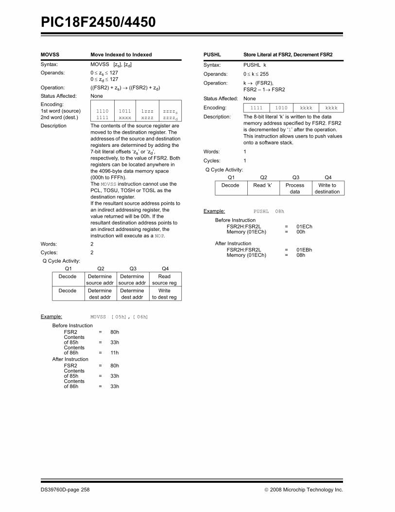
PIC18F2450/4450
DS39760D-page 258 © 2008 Microchip Technology Inc.
MOVSS Move Indexed to Indexed
Syntax: MOVSS [zs], [zd]Operands: 0 ≤ zs ≤ 127
0 ≤ zd ≤ 127Operation: ((FSR2) + zs) → ((FSR2) + zd)Status Affected: NoneEncoding:1st word (source)2nd word (dest.)
11101111
1011xxxx
1zzzxzzz
zzzzszzzzd
Description The contents of the source register are moved to the destination register. The addresses of the source and destination registers are determined by adding the 7-bit literal offsets �zs� or �zd�, respectively, to the value of FSR2. Both registers can be located anywhere in the 4096-byte data memory space (000h to FFFh).The MOVSS instruction cannot use the PCL, TOSU, TOSH or TOSL as the destination register.If the resultant source address points to an indirect addressing register, the value returned will be 00h. If the resultant destination address points to an indirect addressing register, the instruction will execute as a NOP.
Words: 2Cycles: 2Q Cycle Activity:
Q1 Q2 Q3 Q4Decode Determine
source addrDetermine
source addrRead
source regDecode Determine
dest addrDeterminedest addr
Write to dest reg
Example: MOVSS [05h], [06h]
Before InstructionFSR2 = 80hContentsof 85h = 33hContentsof 86h = 11h
After InstructionFSR2 = 80hContentsof 85h = 33hContentsof 86h = 33h
PUSHL Store Literal at FSR2, Decrement FSR2
Syntax: PUSHL k
Operands: 0 ≤ k ≤ 255
Operation: k → (FSR2),FSR2 � 1→ FSR2
Status Affected: None
Encoding: 1111 1010 kkkk kkkk
Description: The 8-bit literal �k� is written to the data memory address specified by FSR2. FSR2 is decremented by �1� after the operation. This instruction allows users to push values onto a software stack.
Words: 1
Cycles: 1
Q Cycle Activity:Q1 Q2 Q3 Q4
Decode Read �k� Processdata
Write todestination
Example: PUSHL 08h
Before InstructionFSR2H:FSR2L = 01EChMemory (01ECh) = 00h
After InstructionFSR2H:FSR2L = 01EBhMemory (01ECh) = 08h
PIC18F2450/4450
© 2008 Microchip Technology Inc. DS39760D-page 259
SUBFSR Subtract Literal from FSR
Syntax: SUBFSR f, kOperands: 0 ≤ k ≤ 63
f ∈ [ 0, 1, 2 ]Operation: FSRf � k → FSRfStatus Affected: NoneEncoding: 1110 1001 ffkk kkkk
Description: The 6-bit literal �k� is subtracted from the contents of the FSR specified by �f�.
Words: 1Cycles: 1Q Cycle Activity:
Q1 Q2 Q3 Q4Decode Read
register �f�Process
DataWrite to
destination
Example: SUBFSR 2, 23h
Before InstructionFSR2 = 03FFh
After InstructionFSR2 = 03DCh
SUBULNK Subtract Literal from FSR2 and Return
Syntax: SUBULNK kOperands: 0 ≤ k ≤ 63Operation: FSR2 � k → FSR2,
(TOS) → PCStatus Affected: NoneEncoding: 1110 1001 11kk kkkk
Description: The 6-bit literal �k� is subtracted from the contents of the FSR2. A RETURN is then executed by loading the PC with the TOS. The instruction takes two cycles to execute; a NOP is performed during the second cycle.This may be thought of as a special case of the SUBFSR instruction, where f = 3 (binary �11�); it operates only on FSR2.
Words: 1Cycles: 2Q Cycle Activity:
Q1 Q2 Q3 Q4Decode Read
register �f�Process
DataWrite to
destinationNo
OperationNo
OperationNo
OperationNo
Operation
Example: SUBULNK 23h
Before InstructionFSR2 = 03FFhPC = 0100h
After InstructionFSR2 = 03DChPC = (TOS)
PIC18F2450/4450
DS39760D-page 260 © 2008 Microchip Technology Inc.
19.2.3 BYTE-ORIENTED AND BIT-ORIENTED INSTRUCTIONS IN INDEXED LITERAL OFFSET MODE
In addition to eight new commands in the extended set,enabling the extended instruction set also enablesIndexed Literal Offset Addressing mode (Section 5.6.1�Indexed Addressing with Literal Offset�). This hasa significant impact on the way that many commands ofthe standard PIC18 instruction set are interpreted.
When the extended set is disabled, addressesembedded in opcodes are treated as literal memorylocations: either as a location in the Access Bank(�a� = 0) or in a GPR bank designated by the BSR(�a� = 1). When the extended instruction set is enabledand �a� = 0, however, a file register argument of 5Fh orless is interpreted as an offset from the pointer value inFSR2 and not as a literal address. For practicalpurposes, this means that all instructions that use theAccess RAM bit as an argument � that is, all byte-oriented and bit-oriented instructions, or almost half ofthe core PIC18 instructions � may behave differentlywhen the extended instruction set is enabled.
When the content of FSR2 is 00h, the boundaries of theAccess RAM are essentially remapped to their originalvalues. This may be useful in creating backwardcompatible code. If this technique is used, it may benecessary to save the value of FSR2 and restore itwhen moving back and forth between C and assemblyroutines in order to preserve the Stack Pointer. Usersmust also keep in mind the syntax requirements of theextended instruction set (see Section 19.2.3.1�Extended Instruction Syntax with Standard PIC18Commands�).
Although the Indexed Literal Offset Addressing modecan be very useful for dynamic stack and pointermanipulation, it can also be very annoying if a simplearithmetic operation is carried out on the wrongregister. Users who are accustomed to the PIC18programming must keep in mind that, when theextended instruction set is enabled, register addressesof 5Fh or less are used for Indexed Literal OffsetAddressing.
Representative examples of typical byte-oriented andbit-oriented instructions in the Indexed Literal OffsetAddressing mode are provided on the following page toshow how execution is affected. The operandconditions shown in the examples are applicable to allinstructions of these types.
19.2.3.1 Extended Instruction Syntax with Standard PIC18 Commands
When the extended instruction set is enabled, the fileregister argument, �f�, in the standard byte-oriented andbit-oriented commands is replaced with the literal offsetvalue, �k�. As already noted, this occurs only when �f� isless than or equal to 5Fh. When an offset value is used,it must be indicated by square brackets (�[ ]�). As withthe extended instructions, the use of brackets indicatesto the compiler that the value is to be interpreted as anindex or an offset. Omitting the brackets, or using avalue greater than 5Fh within brackets, will generate anerror in the MPASM Assembler.
If the index argument is properly bracketed for IndexedLiteral Offset Addressing mode, the Access RAMargument is never specified; it will automatically beassumed to be �0�. This is in contrast to standardoperation (extended instruction set disabled) when �a�is set on the basis of the target address. Declaring theAccess RAM bit in this mode will also generate an errorin the MPASM Assembler.
The destination argument, �d�, functions as before.
In the latest versions of the MPASM assembler,language support for the extended instruction set mustbe explicitly invoked. This is done with either thecommand line option, /y, or the PE directive in thesource listing.
19.2.4 CONSIDERATIONS WHEN ENABLING THE EXTENDED INSTRUCTION SET
It is important to note that the extensions to theinstruction set may not be beneficial to all users. Inparticular, users who are not writing code that uses asoftware stack may not benefit from using theextensions to the instruction set.
Additionally, the Indexed Literal Offset Addressingmode may create issues with legacy applicationswritten to the PIC18 assembler. This is becauseinstructions in the legacy code may attempt to addressregisters in the Access Bank below 5Fh. Since theseaddresses are interpreted as literal offsets to FSR2when the instruction set extension is enabled, theapplication may read or write to the wrong dataaddresses.
When porting an application to the PIC18F2450/4450,it is very important to consider the type of code. A large,re-entrant application that is written in �C� and wouldbenefit from efficient compilation will do well whenusing the instruction set extensions. Legacy applica-tions that heavily use the Access Bank will most likelynot benefit from using the extended instruction set.
Note: Enabling the PIC18 instruction setextension may cause legacy applicationsto behave erratically or fail entirely.

PIC18F2450/4450
© 2008 Microchip Technology Inc. DS39760D-page 261
ADDWF ADD W to Indexed(Indexed Literal Offset mode)
Syntax: ADDWF [k] {,d}
Operands: 0 ≤ k ≤ 95d ∈ [0,1]
Operation: (W) + ((FSR2) + k) → dest
Status Affected: N, OV, C, DC, Z
Encoding: 0010 01d0 kkkk kkkk
Description: The contents of W are added to the contents of the register indicated by FSR2, offset by the value �k�. If �d� is �0�, the result is stored in W. If �d� is �1�, the result is stored back in register �f� (default).
Words: 1
Cycles: 1
Q Cycle Activity:Q1 Q2 Q3 Q4
Decode Read �k� Process Data
Write todestination
Example: ADDWF [OFST] ,0
Before InstructionW = 17hOFST = 2ChFSR2 = 0A00hContentsof 0A2Ch = 20h
After InstructionW = 37hContentsof 0A2Ch = 20h
BSF Bit Set Indexed (Indexed Literal Offset mode)
Syntax: BSF [k], b
Operands: 0 ≤ f ≤ 950 ≤ b ≤ 7
Operation: 1 → ((FSR2) + k)<b>
Status Affected: None
Encoding: 1000 bbb0 kkkk kkkk
Description: Bit �b� of the register indicated by FSR2, offset by the value �k�, is set.
Words: 1
Cycles: 1
Q Cycle Activity:Q1 Q2 Q3 Q4
Decode Readregister �f�
Process Data
Write todestination
Example: BSF [FLAG_OFST], 7
Before InstructionFLAG_OFST = 0AhFSR2 = 0A00hContents of 0A0Ah = 55h
After InstructionContentsof 0A0Ah = D5h
SETF Set Indexed(Indexed Literal Offset mode)
Syntax: SETF [k]
Operands: 0 ≤ k ≤ 95
Operation: FFh → ((FSR2) + k)
Status Affected: None
Encoding: 0110 1000 kkkk kkkk
Description: The contents of the register indicated by FSR2, offset by �k�, are set to FFh.
Words: 1
Cycles: 1
Q Cycle Activity:Q1 Q2 Q3 Q4
Decode Read �k� Process Data
Writeregister
Example: SETF [OFST]
Before InstructionOFST = 2ChFSR2 = 0A00hContentsof 0A2Ch = 00h
After InstructionContentsof 0A2Ch = FFh
PIC18F2450/4450
DS39760D-page 262 © 2008 Microchip Technology Inc.
19.2.5 SPECIAL CONSIDERATIONS WITH MICROCHIP MPLAB® IDE TOOLS
The latest versions of Microchip�s software tools havebeen designed to fully support the extended instructionset of the PIC18F2450/4450 family of devices. Thisincludes the MPLAB C18 C compiler, MPASMAssembly language and MPLAB IntegratedDevelopment Environment (IDE).
When selecting a target device for softwaredevelopment, MPLAB IDE will automatically set defaultConfiguration bits for that device. The default setting forthe XINST Configuration bit is �0�, disabling theextended instruction set and Indexed Literal OffsetAddressing mode. For proper execution of applicationsdeveloped to take advantage of the extendedinstruction set, XINST must be set duringprogramming.
To develop software for the extended instruction set,the user must enable support for the instructions andthe Indexed Addressing mode in their language tool(s).Depending on the environment being used, this may bedone in several ways:
� A menu option, or dialog box within the environment, that allows the user to configure the language tool and its settings for the project
� A command line option� A directive in the source code
These options vary between different compilers,assemblers and development environments. Users areencouraged to review the documentation accompany-ing their development systems for the appropriateinformation.
© 2008 Microchip Technology Inc. DS39760D-page 263
PIC18F2450/4450
20.0 DEVELOPMENT SUPPORTThe PIC® microcontrollers are supported with a fullrange of hardware and software development tools:
� Integrated Development Environment- MPLAB® IDE Software
� Assemblers/Compilers/Linkers- MPASMTM Assembler- MPLAB C18 and MPLAB C30 C Compilers- MPLINKTM Object Linker/
MPLIBTM Object Librarian- MPLAB ASM30 Assembler/Linker/Library
� Simulators- MPLAB SIM Software Simulator
� Emulators- MPLAB ICE 2000 In-Circuit Emulator- MPLAB REAL ICE� In-Circuit Emulator
� In-Circuit Debugger- MPLAB ICD 2
� Device Programmers- PICSTART® Plus Development Programmer- MPLAB PM3 Device Programmer- PICkit� 2 Development Programmer
� Low-Cost Demonstration and Development Boards and Evaluation Kits
20.1 MPLAB Integrated Development Environment Software
The MPLAB IDE software brings an ease of softwaredevelopment previously unseen in the 8/16-bit micro-controller market. The MPLAB IDE is a Windows®
operating system-based application that contains:
� A single graphical interface to all debugging tools- Simulator- Programmer (sold separately)- Emulator (sold separately)- In-Circuit Debugger (sold separately)
� A full-featured editor with color-coded context� A multiple project manager� Customizable data windows with direct edit of
contents� High-level source code debugging� Visual device initializer for easy register
initialization� Mouse over variable inspection� Drag and drop variables from source to watch
windows� Extensive on-line help� Integration of select third party tools, such as
HI-TECH Software C Compilers and IAR C Compilers
The MPLAB IDE allows you to:
� Edit your source files (either assembly or C)� One touch assemble (or compile) and download
to PIC MCU emulator and simulator tools (automatically updates all project information)
� Debug using:- Source files (assembly or C)- Mixed assembly and C- Machine code
MPLAB IDE supports multiple debugging tools in asingle development paradigm, from the cost-effectivesimulators, through low-cost in-circuit debuggers, tofull-featured emulators. This eliminates the learningcurve when upgrading to tools with increased flexibilityand power.

PIC18F2450/4450
DS39760D-page 264 © 2008 Microchip Technology Inc.
20.2 MPASM AssemblerThe MPASM Assembler is a full-featured, universalmacro assembler for all PIC MCUs.
The MPASM Assembler generates relocatable objectfiles for the MPLINK Object Linker, Intel® standard HEXfiles, MAP files to detail memory usage and symbolreference, absolute LST files that contain source linesand generated machine code and COFF files fordebugging.
The MPASM Assembler features include:
� Integration into MPLAB IDE projects� User-defined macros to streamline
assembly code� Conditional assembly for multi-purpose
source files� Directives that allow complete control over the
assembly process
20.3 MPLAB C18 and MPLAB C30 C Compilers
The MPLAB C18 and MPLAB C30 Code DevelopmentSystems are complete ANSI C compilers forMicrochip�s PIC18 and PIC24 families of microcontrol-lers and the dsPIC30 and dsPIC33 family of digital sig-nal controllers. These compilers provide powerfulintegration capabilities, superior code optimization andease of use not found with other compilers.
For easy source level debugging, the compilers providesymbol information that is optimized to the MPLAB IDEdebugger.
20.4 MPLINK Object Linker/MPLIB Object Librarian
The MPLINK Object Linker combines relocatableobjects created by the MPASM Assembler and theMPLAB C18 C Compiler. It can link relocatable objectsfrom precompiled libraries, using directives from alinker script.
The MPLIB Object Librarian manages the creation andmodification of library files of precompiled code. Whena routine from a library is called from a source file, onlythe modules that contain that routine will be linked inwith the application. This allows large libraries to beused efficiently in many different applications.
The object linker/library features include:
� Efficient linking of single libraries instead of many smaller files
� Enhanced code maintainability by grouping related modules together
� Flexible creation of libraries with easy module listing, replacement, deletion and extraction
20.5 MPLAB ASM30 Assembler, Linker and Librarian
MPLAB ASM30 Assembler produces relocatablemachine code from symbolic assembly language fordsPIC30F devices. MPLAB C30 C Compiler uses theassembler to produce its object file. The assemblergenerates relocatable object files that can then bearchived or linked with other relocatable object files andarchives to create an executable file. Notable featuresof the assembler include:
� Support for the entire dsPIC30F instruction set� Support for fixed-point and floating-point data� Command line interface� Rich directive set� Flexible macro language� MPLAB IDE compatibility
20.6 MPLAB SIM Software SimulatorThe MPLAB SIM Software Simulator allows codedevelopment in a PC-hosted environment by simulat-ing the PIC MCUs and dsPIC® DSCs on an instructionlevel. On any given instruction, the data areas can beexamined or modified and stimuli can be applied froma comprehensive stimulus controller. Registers can belogged to files for further run-time analysis. The tracebuffer and logic analyzer display extend the power ofthe simulator to record and track program execution,actions on I/O, most peripherals and internal registers.
The MPLAB SIM Software Simulator fully supportssymbolic debugging using the MPLAB C18 andMPLAB C30 C Compilers, and the MPASM andMPLAB ASM30 Assemblers. The software simulatoroffers the flexibility to develop and debug code outsideof the hardware laboratory environment, making it anexcellent, economical software development tool.

© 2008 Microchip Technology Inc. DS39760D-page 265
PIC18F2450/445020.7 MPLAB ICE 2000
High-Performance In-Circuit Emulator
The MPLAB ICE 2000 In-Circuit Emulator is intendedto provide the product development engineer with acomplete microcontroller design tool set for PICmicrocontrollers. Software control of the MPLAB ICE2000 In-Circuit Emulator is advanced by the MPLABIntegrated Development Environment, which allowsediting, building, downloading and source debuggingfrom a single environment.
The MPLAB ICE 2000 is a full-featured emulatorsystem with enhanced trace, trigger and data monitor-ing features. Interchangeable processor modules allowthe system to be easily reconfigured for emulation ofdifferent processors. The architecture of the MPLABICE 2000 In-Circuit Emulator allows expansion tosupport new PIC microcontrollers.
The MPLAB ICE 2000 In-Circuit Emulator system hasbeen designed as a real-time emulation system withadvanced features that are typically found on moreexpensive development tools. The PC platform andMicrosoft® Windows® 32-bit operating system werechosen to best make these features available in asimple, unified application.
20.8 MPLAB REAL ICE In-Circuit Emulator System
MPLAB REAL ICE In-Circuit Emulator System isMicrochip�s next generation high-speed emulator forMicrochip Flash DSC and MCU devices. It debugs andprograms PIC® Flash MCUs and dsPIC® Flash DSCswith the easy-to-use, powerful graphical user interface ofthe MPLAB Integrated Development Environment (IDE),included with each kit.
The MPLAB REAL ICE probe is connected to the designengineer�s PC using a high-speed USB 2.0 interface andis connected to the target with either a connectorcompatible with the popular MPLAB ICD 2 system(RJ11) or with the new high-speed, noise tolerant, Low-Voltage Differential Signal (LVDS) interconnection(CAT5).
MPLAB REAL ICE is field upgradeable through futurefirmware downloads in MPLAB IDE. In upcomingreleases of MPLAB IDE, new devices will be supported,and new features will be added, such as software break-points and assembly code trace. MPLAB REAL ICEoffers significant advantages over competitive emulatorsincluding low-cost, full-speed emulation, real-timevariable watches, trace analysis, complex breakpoints, aruggedized probe interface and long (up to three meters)interconnection cables.
20.9 MPLAB ICD 2 In-Circuit DebuggerMicrochip�s In-Circuit Debugger, MPLAB ICD 2, is apowerful, low-cost, run-time development tool,connecting to the host PC via an RS-232 or high-speedUSB interface. This tool is based on the Flash PICMCUs and can be used to develop for these and otherPIC MCUs and dsPIC DSCs. The MPLAB ICD 2 utilizesthe in-circuit debugging capability built into the Flashdevices. This feature, along with Microchip�s In-CircuitSerial ProgrammingTM (ICSPTM) protocol, offers cost-effective, in-circuit Flash debugging from the graphicaluser interface of the MPLAB Integrated DevelopmentEnvironment. This enables a designer to develop anddebug source code by setting breakpoints, single step-ping and watching variables, and CPU status andperipheral registers. Running at full speed enablestesting hardware and applications in real time. MPLABICD 2 also serves as a development programmer forselected PIC devices.
20.10 MPLAB PM3 Device ProgrammerThe MPLAB PM3 Device Programmer is a universal,CE compliant device programmer with programmablevoltage verification at VDDMIN and VDDMAX formaximum reliability. It features a large LCD display(128 x 64) for menus and error messages and a modu-lar, detachable socket assembly to support variouspackage types. The ICSP� cable assembly is includedas a standard item. In Stand-Alone mode, the MPLABPM3 Device Programmer can read, verify and programPIC devices without a PC connection. It can also setcode protection in this mode. The MPLAB PM3connects to the host PC via an RS-232 or USB cable.The MPLAB PM3 has high-speed communications andoptimized algorithms for quick programming of largememory devices and incorporates an SD/MMC card forfile storage and secure data applications.
PIC18F2450/4450
DS39760D-page 266 © 2008 Microchip Technology Inc.
20.11 PICSTART Plus Development Programmer
The PICSTART Plus Development Programmer is aneasy-to-use, low-cost, prototype programmer. Itconnects to the PC via a COM (RS-232) port. MPLABIntegrated Development Environment software makesusing the programmer simple and efficient. ThePICSTART Plus Development Programmer supportsmost PIC devices in DIP packages up to 40 pins.Larger pin count devices, such as the PIC16C92X andPIC17C76X, may be supported with an adapter socket.The PICSTART Plus Development Programmer is CEcompliant.
20.12 PICkit 2 Development ProgrammerThe PICkit� 2 Development Programmer is a low-costprogrammer and selected Flash device debugger withan easy-to-use interface for programming many ofMicrochip�s baseline, mid-range and PIC18F families ofFlash memory microcontrollers. The PICkit 2 Starter Kitincludes a prototyping development board, twelvesequential lessons, software and HI-TECH�s PICC�Lite C compiler, and is designed to help get up to speedquickly using PIC® microcontrollers. The kit provideseverything needed to program, evaluate and developapplications using Microchip�s powerful, mid-rangeFlash memory family of microcontrollers.
20.13 Demonstration, Development and Evaluation Boards
A wide variety of demonstration, development andevaluation boards for various PIC MCUs and dsPICDSCs allows quick application development on fully func-tional systems. Most boards include prototyping areas foradding custom circuitry and provide application firmwareand source code for examination and modification.
The boards support a variety of features, including LEDs,temperature sensors, switches, speakers, RS-232interfaces, LCD displays, potentiometers and additionalEEPROM memory.
The demonstration and development boards can beused in teaching environments, for prototyping customcircuits and for learning about various microcontrollerapplications.
In addition to the PICDEM� and dsPICDEM� demon-stration/development board series of circuits, Microchiphas a line of evaluation kits and demonstration softwarefor analog filter design, KEELOQ® security ICs, CAN,IrDA®, PowerSmart battery management, SEEVAL®
evaluation system, Sigma-Delta ADC, flow ratesensing, plus many more.
Check the Microchip web page (www.microchip.com)for the complete list of demonstration, developmentand evaluation kits.
PIC18F2450/4450
© 2008 Microchip Technology Inc. DS39760D-page 267
21.0 ELECTRICAL CHARACTERISTICS
Absolute Maximum Ratings(�) Ambient temperature under bias.............................................................................................................. .-40°C to +85°C
Storage temperature .............................................................................................................................. -65°C to +150°C
Voltage on any pin with respect to VSS (except VDD and MCLR) ................................................... -0.3V to (VDD + 0.3V)
Voltage on VDD with respect to VSS ......................................................................................................... -0.3V to +7.5V
Voltage on MCLR with respect to VSS (Note 2) ......................................................................................... 0V to +13.25V
Total power dissipation (Note 1) ...............................................................................................................................1.0W
Maximum current out of VSS pin ...........................................................................................................................300 mA
Maximum current into VDD pin ..............................................................................................................................250 mA
Input clamp current, IIK (VI < 0 or VI > VDD)...................................................................................................................... ±20 mA
Output clamp current, IOK (VO < 0 or VO > VDD) .............................................................................................................. ±20 mA
Maximum output current sunk by any I/O pin..........................................................................................................25 mA
Maximum output current sourced by any I/O pin ....................................................................................................25 mA
Maximum current sunk by all ports .......................................................................................................................200 mA
Maximum current sourced by all ports ..................................................................................................................200 mA
Note 1: Power dissipation is calculated as follows: Pdis = VDD x {IDD � ∑ IOH} + ∑ {(VDD � VOH) x IOH} + ∑(VOL x IOL)
2: Voltage spikes below VSS at the MCLR/VPP/RE3 pin, inducing currents greater than 80 mA, may causelatch-up. Thus, a series resistor of 50-100Ω should be used when applying a �low� level to the MCLR/VPP/RE3 pin, rather than pulling this pin directly to VSS.
� NOTICE: Stresses above those listed under �Absolute Maximum Ratings� may cause permanent damage to the device. This is a stress rating only and functional operation of the device at those or any other conditions above those indicated in the operation listings of this specification is not implied. Exposure to maximum rating conditions for extended periods may affect device reliability.
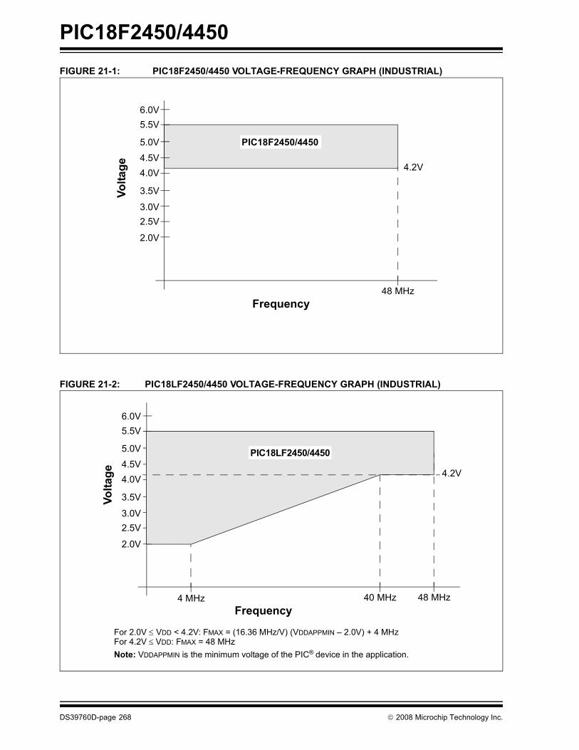
PIC18F2450/4450
DS39760D-page 268 © 2008 Microchip Technology Inc.
FIGURE 21-1: PIC18F2450/4450 VOLTAGE-FREQUENCY GRAPH (INDUSTRIAL)
FIGURE 21-2: PIC18LF2450/4450 VOLTAGE-FREQUENCY GRAPH (INDUSTRIAL)
Frequency
Volta
ge6.0V5.5V
4.5V4.0V
2.0V
48 MHz
5.0V
3.5V
3.0V2.5V
PIC18F2450/4450
4.2V
Frequency
Volta
ge
6.0V5.5V
4.5V4.0V
2.0V
40 MHz
5.0V
3.5V
3.0V2.5V
For 2.0V ≤ VDD < 4.2V: FMAX = (16.36 MHz/V) (VDDAPPMIN � 2.0V) + 4 MHz
Note: VDDAPPMIN is the minimum voltage of the PIC® device in the application.
4 MHz
4.2V
48 MHz
PIC18LF2450/4450
For 4.2V ≤ VDD: FMAX = 48 MHz

PIC18F2450/4450
© 2008 Microchip Technology Inc. DS39760D-page 269
21.1 DC Characteristics: Supply VoltagePIC18F2450/4450 (Industrial) PIC18LF2450/4450 (Industrial)
PIC18LF2450/4450 (Industrial)
Standard Operating Conditions (unless otherwise stated)Operating temperature -40°C ≤ TA ≤ +85°C for industrial
PIC18F2450/4450 (Industrial)
Standard Operating Conditions (unless otherwise stated)Operating temperature -40°C ≤ TA ≤ +85°C for industrial
Param No. Symbol Characteristic Min Typ Max Units Conditions
D001 VDD Supply Voltage 2.0 � 5.5 V EC, HS, XT and Internal Oscillator modes3.0 � 5.5 V HSPLL, XTPLL, ECPIO and ECPLL
Oscillator modesD002 VDR RAM Data Retention
Voltage(1)1.5 � � V
D003 VPOR VDD Start Voltage to ensure internal Power-on Reset signal
� � 0.7 V See Section 4.3 �Power-on Reset (POR)� for details
D004 SVDD VDD Rise Rateto Ensure Internal Power-on Reset Signal
0.05 � � V/ms See Section 4.3 �Power-on Reset (POR)� for details
D005 VBOR Brown-out Reset VoltageBORV1:BORV0 = 11 2.00 2.11 2.22 VBORV1:BORV0 = 10 2.65 2.79 2.93 VBORV1:BORV0 = 01 4.11 4.33 4.55 VBORV1:BORV0 = 00 4.36 4.59 4.82 V
Legend: Shading of rows is to assist in readability of the table.Note 1: This is the limit to which VDD can be lowered in Sleep mode, or during a device Reset, without losing RAM data.

PIC18F2450/4450
DS39760D-page 270 © 2008 Microchip Technology Inc.
21.2 DC Characteristics: Power-Down and Supply CurrentPIC18F2450/4450 (Industrial) PIC18LF2450/4450 (Industrial)
PIC18LF2450/4450 (Industrial)
Standard Operating Conditions (unless otherwise stated)Operating temperature -40°C ≤ TA ≤ +85°C for industrial
PIC18F2450/4450 (Industrial)
Standard Operating Conditions (unless otherwise stated)Operating temperature -40°C ≤ TA ≤ +85°C for industrial
Param No. Device Typ Max Units Conditions
Power-Down Current (IPD)(1)
PIC18LF2450/4450 0.1 0.95 μA -40°CVDD = 2.0V
(Sleep mode)0.1 1.0 μA +25°C0.1 5.0 μA +85°C
PIC18LF2450/4450 0.1 1.4 μA -40°CVDD = 3.0V
(Sleep mode)0.1 2.0 μA +25°C1.5 8.0 μA +85°C
All devices 0.1 19 μA -40°CVDD = 5.0V
(Sleep mode)0.1 2.0 μA +25°C2.5 15 μA +85°C
Legend: Shading of rows is to assist in readability of the table.Note 1: The power-down current in Sleep mode does not depend on the oscillator type. Power-down current is measured
with the part in Sleep mode, with all I/O pins in high-impedance state and tied to VDD or VSS and all features that add delta current disabled (such as WDT, Timer1 Oscillator, BOR, etc.).
2: The supply current is mainly a function of operating voltage, frequency and mode. Other factors, such as I/O pin loading and switching rate, oscillator type and circuit, internal code execution pattern and temperature, also have an impact on the current consumption.The test conditions for all IDD measurements in active operation mode are:
OSC1 = external square wave, from rail-to-rail; all I/O pins tri-stated, pulled to VDD or VSS;MCLR = VDD; WDT enabled/disabled as specified.
3: Standard low-cost 32 kHz crystals have an operating temperature range of -10°C to +70°C. Extended temperature crystals are available at a much higher cost.
4: BOR and HLVD enable internal band gap reference. With both modules enabled, current consumption will be less than the sum of both specifications.

PIC18F2450/4450
© 2008 Microchip Technology Inc. DS39760D-page 271
Supply Current (IDD)(2)
PIC18LF2450/4450 10 32 μA -40°CVDD = 2.0V
FOSC = 31 kHz(RC_RUN mode, INTRC source)
10 30 μA +25°C12 29 μA +85°C
PIC18LF2450/4450 35 63 μA -40°CVDD = 3.0V30 60 μA +25°C
25 57 μA +85°CAll devices 95 168 μA -40°C
VDD = 5.0V75 160 μA +25°C65 152 μA +85°C
PIC18LF2450/4450 2.3 8 μA -40°CVDD = 2.0V
FOSC = 31 kHz(RC_IDLE mode, INTRC source)
2.5 8 μA +25°C3.3 11 μA +85°C
PIC18LF2450/4450 3.3 11 μA -40°CVDD = 3.0V3.6 11 μA +25°C
4.0 15 μA +85°CAll devices 6.5 16 μA -40°C
VDD = 5.0V7.0 16 μA +25°C9.0 36 μA +85°C
21.2 DC Characteristics: Power-Down and Supply CurrentPIC18F2450/4450 (Industrial) PIC18LF2450/4450 (Industrial) (Continued)
PIC18LF2450/4450 (Industrial)
Standard Operating Conditions (unless otherwise stated)Operating temperature -40°C ≤ TA ≤ +85°C for industrial
PIC18F2450/4450 (Industrial)
Standard Operating Conditions (unless otherwise stated)Operating temperature -40°C ≤ TA ≤ +85°C for industrial
Param No. Device Typ Max Units Conditions
Legend: Shading of rows is to assist in readability of the table.Note 1: The power-down current in Sleep mode does not depend on the oscillator type. Power-down current is measured
with the part in Sleep mode, with all I/O pins in high-impedance state and tied to VDD or VSS and all features that add delta current disabled (such as WDT, Timer1 Oscillator, BOR, etc.).
2: The supply current is mainly a function of operating voltage, frequency and mode. Other factors, such as I/O pin loading and switching rate, oscillator type and circuit, internal code execution pattern and temperature, also have an impact on the current consumption.The test conditions for all IDD measurements in active operation mode are:
OSC1 = external square wave, from rail-to-rail; all I/O pins tri-stated, pulled to VDD or VSS;MCLR = VDD; WDT enabled/disabled as specified.
3: Standard low-cost 32 kHz crystals have an operating temperature range of -10°C to +70°C. Extended temperature crystals are available at a much higher cost.
4: BOR and HLVD enable internal band gap reference. With both modules enabled, current consumption will be less than the sum of both specifications.

PIC18F2450/4450
DS39760D-page 272 © 2008 Microchip Technology Inc.
Supply Current (IDD)(2)
PIC18LF2450/4450 200 500 μA -40°CVDD = 2.0V
FOSC = 1 MHZ(PRI_RUN,
EC oscillator)
200 500 μA +25°C200 500 μA +85°C
PIC18LF2450/4450 500 650 μA -40°CVDD = 3.0V400 650 μA +25°C
360 650 μA +85°CAll devices 1.0 1.6 mA -40°C
VDD = 5.0V0.9 1.5 mA +25°C0.8 1.4 mA +85°C
PIC18LF2450/4450 0.53 2.0 mA -40°CVDD = 2.0V
FOSC = 4 MHz(PRI_RUN,
EC oscillator)
0.53 2.0 mA +25°C0.55 2.0 mA +85°C
PIC18LF2450/4450 1.0 3.0 mA -40°CVDD = 3.0V0.9 3.0 mA +25°C
0.9 3.0 mA +85°CAll devices 2.0 6.0 mA -40°C
VDD = 5.0V1.9 6.0 mA +25°C1.8 6.0 mA +85°C
All devices 11.0 35 mA -40°CVDD = 4.2V
FOSC = 40 MHZ(PRI_RUN,
EC oscillator)
11.0 35 mA +25°C11.3 35 mA +85°C
All devices 14.0 40 mA -40°CVDD = 5.0V14.0 40 mA +25°C
14.5 40 mA +85°CAll devices 20 40 mA -40°C
VDD = 4.2VFOSC = 48 MHZ
(PRI_RUN,EC oscillator)
20 40 mA +25°C20 40 mA +85°C
All devices 25 50 mA -40°CVDD = 5.0V25 50 mA +25°C
25 50 mA +85°C
21.2 DC Characteristics: Power-Down and Supply CurrentPIC18F2450/4450 (Industrial) PIC18LF2450/4450 (Industrial) (Continued)
PIC18LF2450/4450 (Industrial)
Standard Operating Conditions (unless otherwise stated)Operating temperature -40°C ≤ TA ≤ +85°C for industrial
PIC18F2450/4450 (Industrial)
Standard Operating Conditions (unless otherwise stated)Operating temperature -40°C ≤ TA ≤ +85°C for industrial
Param No. Device Typ Max Units Conditions
Legend: Shading of rows is to assist in readability of the table.Note 1: The power-down current in Sleep mode does not depend on the oscillator type. Power-down current is measured
with the part in Sleep mode, with all I/O pins in high-impedance state and tied to VDD or VSS and all features that add delta current disabled (such as WDT, Timer1 Oscillator, BOR, etc.).
2: The supply current is mainly a function of operating voltage, frequency and mode. Other factors, such as I/O pin loading and switching rate, oscillator type and circuit, internal code execution pattern and temperature, also have an impact on the current consumption.The test conditions for all IDD measurements in active operation mode are:
OSC1 = external square wave, from rail-to-rail; all I/O pins tri-stated, pulled to VDD or VSS;MCLR = VDD; WDT enabled/disabled as specified.
3: Standard low-cost 32 kHz crystals have an operating temperature range of -10°C to +70°C. Extended temperature crystals are available at a much higher cost.
4: BOR and HLVD enable internal band gap reference. With both modules enabled, current consumption will be less than the sum of both specifications.

PIC18F2450/4450
© 2008 Microchip Technology Inc. DS39760D-page 273
Supply Current (IDD)(2)
PIC18LF2450/4450 50 130 μA -40°CVDD = 2.0V
FOSC = 1 MHz(PRI_IDLE mode,
EC oscillator)
50 120 μA +25°C50 115 μA +85°C
PIC18LF2450/4450 75 270 μA -40°CVDD = 3.0V80 250 μA +25°C
80 240 μA +85°CAll devices 150 480 μA -40°C
VDD = 5.0V150 450 μA +25°C150 430 μA +85°C
PIC18LF2450/4450 190 475 μA -40°CVDD = 2.0V
FOSC = 4 MHz(PRI_IDLE mode,
EC oscillator)
195 450 μA +25°C200 430 μA +85°C
PIC18LF2450/4450 295 900 μA -40°CVDD = 3.0V300 850 μA +25°C
310 810 μA +85°CAll devices 560 1.5 mA -40°C
VDD = 5.0V570 1.4 mA +25°C580 1.3 mA +85°C
All devices 4.4 16 mA -40°CVDD = 4.2V
FOSC = 40 MHz(PRI_IDLE mode,
EC oscillator)
4.5 16 mA +25°C4.6 16 mA +85°C
All devices 5.5 18 mA -40°CVDD = 5.0V5.6 18 mA +25°C
5.8 18 mA +85°CAll devices 8.0 18 mA -40°C
VDD = 4.2VFOSC = 48 MHz
(PRI_IDLE mode, EC oscillator)
8.1 18 mA +25°C8.2 18 mA +85°C
All devices 9.8 21 mA -40°CVDD = 5.0V10.0 21 mA +25°C
10.5 21 mA +85°C
21.2 DC Characteristics: Power-Down and Supply CurrentPIC18F2450/4450 (Industrial) PIC18LF2450/4450 (Industrial) (Continued)
PIC18LF2450/4450 (Industrial)
Standard Operating Conditions (unless otherwise stated)Operating temperature -40°C ≤ TA ≤ +85°C for industrial
PIC18F2450/4450 (Industrial)
Standard Operating Conditions (unless otherwise stated)Operating temperature -40°C ≤ TA ≤ +85°C for industrial
Param No. Device Typ Max Units Conditions
Legend: Shading of rows is to assist in readability of the table.Note 1: The power-down current in Sleep mode does not depend on the oscillator type. Power-down current is measured
with the part in Sleep mode, with all I/O pins in high-impedance state and tied to VDD or VSS and all features that add delta current disabled (such as WDT, Timer1 Oscillator, BOR, etc.).
2: The supply current is mainly a function of operating voltage, frequency and mode. Other factors, such as I/O pin loading and switching rate, oscillator type and circuit, internal code execution pattern and temperature, also have an impact on the current consumption.The test conditions for all IDD measurements in active operation mode are:
OSC1 = external square wave, from rail-to-rail; all I/O pins tri-stated, pulled to VDD or VSS;MCLR = VDD; WDT enabled/disabled as specified.
3: Standard low-cost 32 kHz crystals have an operating temperature range of -10°C to +70°C. Extended temperature crystals are available at a much higher cost.
4: BOR and HLVD enable internal band gap reference. With both modules enabled, current consumption will be less than the sum of both specifications.

PIC18F2450/4450
DS39760D-page 274 © 2008 Microchip Technology Inc.
Supply Current (IDD)(2)
PIC18LF2450/4450 13 40 μA -40°CVDD = 2.0V
FOSC = 32 kHz(3)
(SEC_RUN mode, Timer1 as clock)
15 40 μA +25°C17 40 μA +85°C
PIC18LF2450/4450 40 76 μA -40°CVDD = 3.0V32 70 μA +25°C
25 67 μA +85°CAll devices 100 150 μA -40°C
VDD = 5.0V80 150 μA +25°C70 150 μA +85°C
PIC18LF2450/4450 5.6 12 μA -40°CVDD = 2.0V
FOSC = 32 kHz(3)
(SEC_IDLE mode, Timer1 as clock)
7.0 12 μA +25°C8.3 12 μA +85°C
PIC18LF2450/4450 6.5 15 μA -40°CVDD = 3.0V8.0 15 μA +25°C
9.5 15 μA +85°CAll devices 8.7 25 μA -40°C
VDD = 5.0V10.2 25 μA +25°C13.0 36 μA +85°C
21.2 DC Characteristics: Power-Down and Supply CurrentPIC18F2450/4450 (Industrial) PIC18LF2450/4450 (Industrial) (Continued)
PIC18LF2450/4450 (Industrial)
Standard Operating Conditions (unless otherwise stated)Operating temperature -40°C ≤ TA ≤ +85°C for industrial
PIC18F2450/4450 (Industrial)
Standard Operating Conditions (unless otherwise stated)Operating temperature -40°C ≤ TA ≤ +85°C for industrial
Param No. Device Typ Max Units Conditions
Legend: Shading of rows is to assist in readability of the table.Note 1: The power-down current in Sleep mode does not depend on the oscillator type. Power-down current is measured
with the part in Sleep mode, with all I/O pins in high-impedance state and tied to VDD or VSS and all features that add delta current disabled (such as WDT, Timer1 Oscillator, BOR, etc.).
2: The supply current is mainly a function of operating voltage, frequency and mode. Other factors, such as I/O pin loading and switching rate, oscillator type and circuit, internal code execution pattern and temperature, also have an impact on the current consumption.The test conditions for all IDD measurements in active operation mode are:
OSC1 = external square wave, from rail-to-rail; all I/O pins tri-stated, pulled to VDD or VSS;MCLR = VDD; WDT enabled/disabled as specified.
3: Standard low-cost 32 kHz crystals have an operating temperature range of -10°C to +70°C. Extended temperature crystals are available at a much higher cost.
4: BOR and HLVD enable internal band gap reference. With both modules enabled, current consumption will be less than the sum of both specifications.
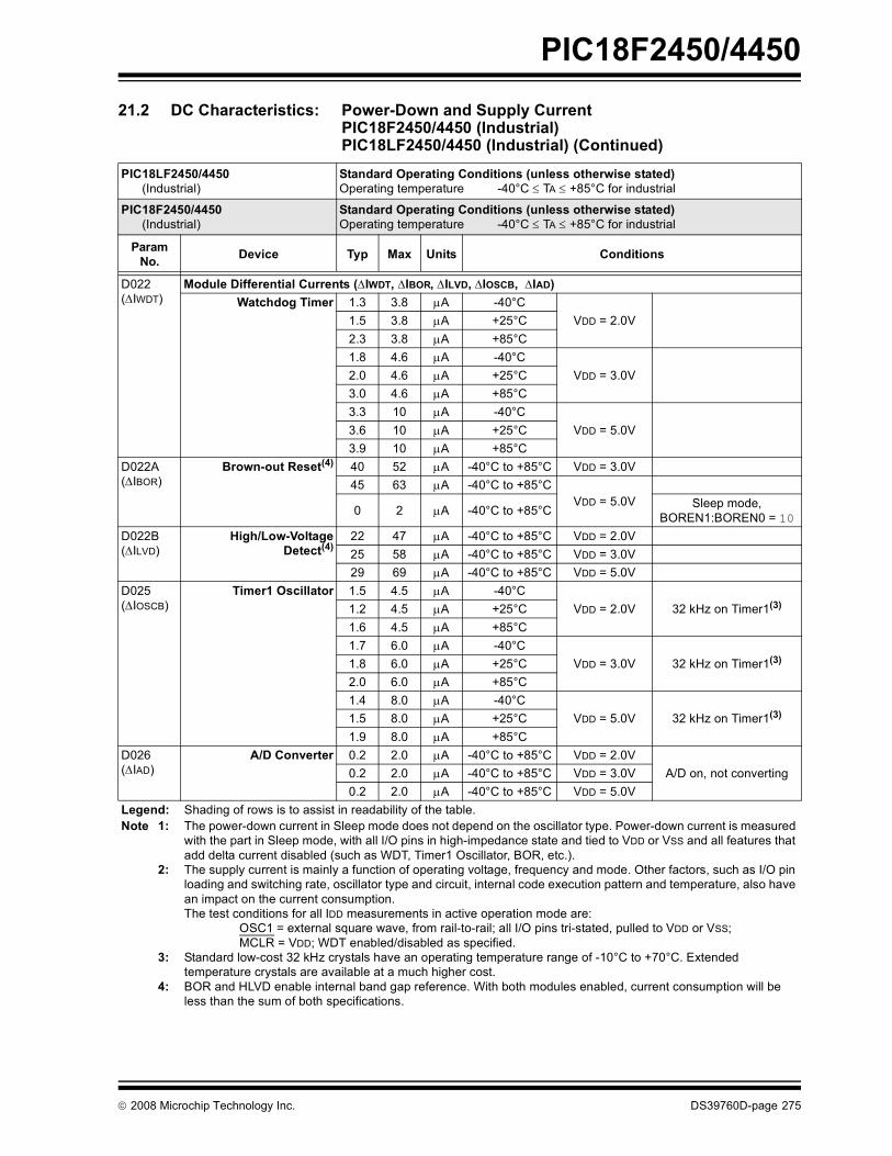
PIC18F2450/4450
© 2008 Microchip Technology Inc. DS39760D-page 275
D022(ΔIWDT)
Module Differential Currents (ΔIWDT, ΔIBOR, ΔILVD, ΔIOSCB, ΔIAD)Watchdog Timer 1.3 3.8 μA -40°C
VDD = 2.0V1.5 3.8 μA +25°C2.3 3.8 μA +85°C1.8 4.6 μA -40°C
VDD = 3.0V2.0 4.6 μA +25°C3.0 4.6 μA +85°C3.3 10 μA -40°C
VDD = 5.0V3.6 10 μA +25°C3.9 10 μA +85°C
D022A(ΔIBOR)
Brown-out Reset(4) 40 52 μA -40°C to +85°C VDD = 3.0V45 63 μA -40°C to +85°C
VDD = 5.0V0 2 μA -40°C to +85°C Sleep mode,
BOREN1:BOREN0 = 10
D022B(ΔILVD)
High/Low-VoltageDetect(4)
22 47 μA -40°C to +85°C VDD = 2.0V25 58 μA -40°C to +85°C VDD = 3.0V29 69 μA -40°C to +85°C VDD = 5.0V
D025(ΔIOSCB)
Timer1 Oscillator 1.5 4.5 μA -40°CVDD = 2.0V 32 kHz on Timer1(3)1.2 4.5 μA +25°C
1.6 4.5 μA +85°C1.7 6.0 μA -40°C
VDD = 3.0V 32 kHz on Timer1(3)1.8 6.0 μA +25°C2.0 6.0 μA +85°C1.4 8.0 μA -40°C
VDD = 5.0V 32 kHz on Timer1(3)1.5 8.0 μA +25°C1.9 8.0 μA +85°C
D026(ΔIAD)
A/D Converter 0.2 2.0 μA -40°C to +85°C VDD = 2.0VA/D on, not converting0.2 2.0 μA -40°C to +85°C VDD = 3.0V
0.2 2.0 μA -40°C to +85°C VDD = 5.0V
21.2 DC Characteristics: Power-Down and Supply CurrentPIC18F2450/4450 (Industrial) PIC18LF2450/4450 (Industrial) (Continued)
PIC18LF2450/4450 (Industrial)
Standard Operating Conditions (unless otherwise stated)Operating temperature -40°C ≤ TA ≤ +85°C for industrial
PIC18F2450/4450 (Industrial)
Standard Operating Conditions (unless otherwise stated)Operating temperature -40°C ≤ TA ≤ +85°C for industrial
Param No. Device Typ Max Units Conditions
Legend: Shading of rows is to assist in readability of the table.Note 1: The power-down current in Sleep mode does not depend on the oscillator type. Power-down current is measured
with the part in Sleep mode, with all I/O pins in high-impedance state and tied to VDD or VSS and all features that add delta current disabled (such as WDT, Timer1 Oscillator, BOR, etc.).
2: The supply current is mainly a function of operating voltage, frequency and mode. Other factors, such as I/O pin loading and switching rate, oscillator type and circuit, internal code execution pattern and temperature, also have an impact on the current consumption.The test conditions for all IDD measurements in active operation mode are:
OSC1 = external square wave, from rail-to-rail; all I/O pins tri-stated, pulled to VDD or VSS;MCLR = VDD; WDT enabled/disabled as specified.
3: Standard low-cost 32 kHz crystals have an operating temperature range of -10°C to +70°C. Extended temperature crystals are available at a much higher cost.
4: BOR and HLVD enable internal band gap reference. With both modules enabled, current consumption will be less than the sum of both specifications.
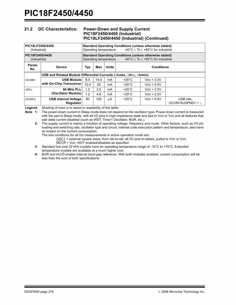
PIC18F2450/4450
DS39760D-page 276 © 2008 Microchip Technology Inc.
USB and Related Module Differential Currents (ΔIUSBx, ΔIPLL, ΔIUREG)ΔIUSBX USB Module
with On-Chip Transceiver8.0 14.5 mA +25°C VDD = 3.3V12.4 20 mA +25°C VDD = 5.0V
ΔIPLL 96 MHz PLL(Oscillator Module)
1.2 3.0 mA +25°C VDD = 3.3V1.2 4.8 mA +25°C VDD = 5.0V
ΔIUREG USB Internal VoltageRegulator
80 125 μA +25°C VDD = 5.0V USB Idle, UCON<SUSPND> = 1
21.2 DC Characteristics: Power-Down and Supply CurrentPIC18F2450/4450 (Industrial) PIC18LF2450/4450 (Industrial) (Continued)
PIC18LF2450/4450 (Industrial)
Standard Operating Conditions (unless otherwise stated)Operating temperature -40°C ≤ TA ≤ +85°C for industrial
PIC18F2450/4450 (Industrial)
Standard Operating Conditions (unless otherwise stated)Operating temperature -40°C ≤ TA ≤ +85°C for industrial
Param No. Device Typ Max Units Conditions
Legend: Shading of rows is to assist in readability of the table.Note 1: The power-down current in Sleep mode does not depend on the oscillator type. Power-down current is measured
with the part in Sleep mode, with all I/O pins in high-impedance state and tied to VDD or VSS and all features that add delta current disabled (such as WDT, Timer1 Oscillator, BOR, etc.).
2: The supply current is mainly a function of operating voltage, frequency and mode. Other factors, such as I/O pin loading and switching rate, oscillator type and circuit, internal code execution pattern and temperature, also have an impact on the current consumption.The test conditions for all IDD measurements in active operation mode are:
OSC1 = external square wave, from rail-to-rail; all I/O pins tri-stated, pulled to VDD or VSS;MCLR = VDD; WDT enabled/disabled as specified.
3: Standard low-cost 32 kHz crystals have an operating temperature range of -10°C to +70°C. Extended temperature crystals are available at a much higher cost.
4: BOR and HLVD enable internal band gap reference. With both modules enabled, current consumption will be less than the sum of both specifications.

PIC18F2450/4450
© 2008 Microchip Technology Inc. DS39760D-page 277
ITUSB Total USB Run Currents (ITUSB)(2)
Primary Run with USBModule, PLL and USB
Voltage Regulator
29 65 mA -40°C VDD = 5.0V EC+PLL 4 MHz input, 48 MHz PRI_RUN,
USB module enabled in Full-Speed mode,
USB VREG enabled, no bus traffic
29 65 mA +25°C VDD = 5.0V29 65 mA +85°C VDD = 5.0V
21.2 DC Characteristics: Power-Down and Supply CurrentPIC18F2450/4450 (Industrial) PIC18LF2450/4450 (Industrial) (Continued)
PIC18LF2450/4450 (Industrial)
Standard Operating Conditions (unless otherwise stated)Operating temperature -40°C ≤ TA ≤ +85°C for industrial
PIC18F2450/4450 (Industrial)
Standard Operating Conditions (unless otherwise stated)Operating temperature -40°C ≤ TA ≤ +85°C for industrial
Param No. Device Typ Max Units Conditions
Legend: Shading of rows is to assist in readability of the table.Note 1: The power-down current in Sleep mode does not depend on the oscillator type. Power-down current is measured
with the part in Sleep mode, with all I/O pins in high-impedance state and tied to VDD or VSS and all features that add delta current disabled (such as WDT, Timer1 Oscillator, BOR, etc.).
2: The supply current is mainly a function of operating voltage, frequency and mode. Other factors, such as I/O pin loading and switching rate, oscillator type and circuit, internal code execution pattern and temperature, also have an impact on the current consumption.The test conditions for all IDD measurements in active operation mode are:
OSC1 = external square wave, from rail-to-rail; all I/O pins tri-stated, pulled to VDD or VSS;MCLR = VDD; WDT enabled/disabled as specified.
3: Standard low-cost 32 kHz crystals have an operating temperature range of -10°C to +70°C. Extended temperature crystals are available at a much higher cost.
4: BOR and HLVD enable internal band gap reference. With both modules enabled, current consumption will be less than the sum of both specifications.
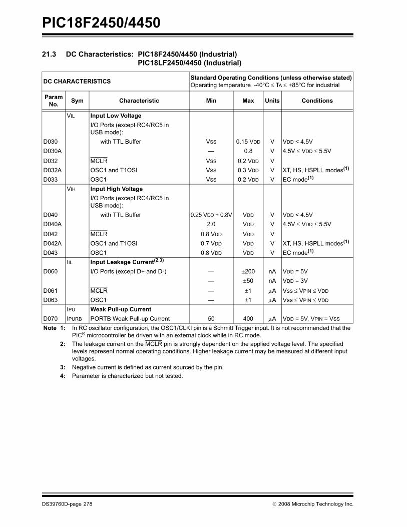
PIC18F2450/4450
DS39760D-page 278 © 2008 Microchip Technology Inc.
21.3 DC Characteristics: PIC18F2450/4450 (Industrial) PIC18LF2450/4450 (Industrial)
DC CHARACTERISTICS Standard Operating Conditions (unless otherwise stated)Operating temperature -40°C ≤ TA ≤ +85°C for industrial
ParamNo. Sym Characteristic Min Max Units Conditions
VIL Input Low VoltageI/O Ports (except RC4/RC5 in USB mode):
D030 with TTL Buffer VSS 0.15 VDD V VDD < 4.5V D030A � 0.8 V 4.5V ≤ VDD ≤ 5.5V
D032 MCLR VSS 0.2 VDD VD032A OSC1 and T1OSI VSS 0.3 VDD V XT, HS, HSPLL modes(1)
D033 OSC1 VSS 0.2 VDD V EC mode(1)
VIH Input High VoltageI/O Ports (except RC4/RC5 in USB mode):
D040 with TTL Buffer 0.25 VDD + 0.8V VDD V VDD < 4.5VD040A 2.0 VDD V 4.5V ≤ VDD ≤ 5.5V
D042 MCLR 0.8 VDD VDD VD042A OSC1 and T1OSI 0.7 VDD VDD V XT, HS, HSPLL modes(1)
D043 OSC1 0.8 VDD VDD V EC mode(1)
IIL Input Leakage Current(2,3) D060 I/O Ports (except D+ and D-) � ±200 nA VDD = 5V
� ±50 nA VDD = 3V
D061 MCLR � ±1 μA Vss ≤ VPIN ≤ VDD
D063 OSC1 � ±1 μA Vss ≤ VPIN ≤ VDD IPU Weak Pull-up Current
D070 IPURB PORTB Weak Pull-up Current 50 400 μA VDD = 5V, VPIN = VSS
Note 1: In RC oscillator configuration, the OSC1/CLKI pin is a Schmitt Trigger input. It is not recommended that the PIC® microcontroller be driven with an external clock while in RC mode.
2: The leakage current on the MCLR pin is strongly dependent on the applied voltage level. The specified levels represent normal operating conditions. Higher leakage current may be measured at different input voltages.
3: Negative current is defined as current sourced by the pin.4: Parameter is characterized but not tested.
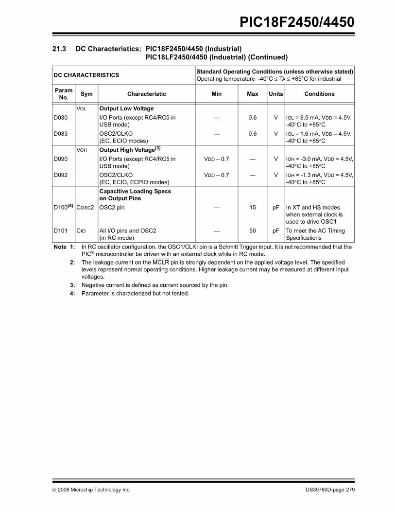
PIC18F2450/4450
© 2008 Microchip Technology Inc. DS39760D-page 279
VOL Output Low VoltageD080 I/O Ports (except RC4/RC5 in
USB mode)� 0.6 V IOL = 8.5 mA, VDD = 4.5V,
-40°C to +85°CD083 OSC2/CLKO
(EC, ECIO modes)� 0.6 V IOL = 1.6 mA, VDD = 4.5V,
-40°C to +85°CVOH Output High Voltage(3)
D090 I/O Ports (except RC4/RC5 in USB mode)
VDD � 0.7 � V IOH = -3.0 mA, VDD = 4.5V,-40°C to +85°C
D092 OSC2/CLKO (EC, ECIO, ECPIO modes)
VDD � 0.7 � V IOH = -1.3 mA, VDD = 4.5V,-40°C to +85°C
Capacitive Loading Specson Output Pins
D100(4) COSC2 OSC2 pin � 15 pF In XT and HS modes when external clock is used to drive OSC1
D101 CIO All I/O pins and OSC2 (in RC mode)
� 50 pF To meet the AC Timing Specifications
21.3 DC Characteristics: PIC18F2450/4450 (Industrial) PIC18LF2450/4450 (Industrial) (Continued)
DC CHARACTERISTICS Standard Operating Conditions (unless otherwise stated)Operating temperature -40°C ≤ TA ≤ +85°C for industrial
ParamNo. Sym Characteristic Min Max Units Conditions
Note 1: In RC oscillator configuration, the OSC1/CLKI pin is a Schmitt Trigger input. It is not recommended that the PIC® microcontroller be driven with an external clock while in RC mode.
2: The leakage current on the MCLR pin is strongly dependent on the applied voltage level. The specified levels represent normal operating conditions. Higher leakage current may be measured at different input voltages.
3: Negative current is defined as current sourced by the pin.4: Parameter is characterized but not tested.

PIC18F2450/4450
DS39760D-page 280 © 2008 Microchip Technology Inc.
TABLE 21-1: MEMORY PROGRAMMING REQUIREMENTS
DC Characteristics Standard Operating Conditions (unless otherwise stated)Operating temperature -40°C ≤ TA ≤ +85°C for industrial
ParamNo. Sym Characteristic Min Typ� Max Units Conditions
Internal Program Memory Programming Specifications(1)
D110 VIHH Voltage on MCLR/VPP/RE3 pin 9.00 � 13.25 V (Note 2)D113 IDDP Supply Current during
Programming� � 10 mA
Program Flash MemoryD130 EP Cell Endurance 10K 100K � E/W -40°C to +85°CD131 VPR VDD for Read VMIN � 5.5 V VMIN = Minimum operating
voltageD132 VIE VDD for Block Erase 4.5 � 5.5 V Using ICSP� portD132A VIW VDD for Externally Timed Erase
or Write3.0 � 5.5 V Using ICSP port
D132B VPEW VDD for Self-Timed Write VMIN � 5.5 V VMIN = Minimum operating voltage
D133 TIE ICSP� Block Erase Cycle Time � 4 � ms VDD > 4.5VD133A TIW ICSP Erase or Write Cycle Time
(externally timed)1 � � ms VDD > 4.5V
D133A TIW Self-Timed Write Cycle Time � 2 � msD134 TRETD Characteristic Retention 40 100 � Year Provided no other
specifications are violated� Data in �Typ� column is at 5.0V, 25°C unless otherwise stated. These parameters are for design guidance
only and are not tested.Note 1: These specifications are for programming the on-chip program memory through the use of table write
instructions.2: Required only if Single-Supply Programming is disabled.
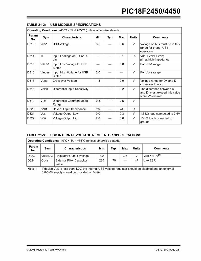
PIC18F2450/4450
© 2008 Microchip Technology Inc. DS39760D-page 281
TABLE 21-2: USB MODULE SPECIFICATIONS
TABLE 21-3: USB INTERNAL VOLTAGE REGULATOR SPECIFICATIONS
Operating Conditions: -40°C < TA < +85°C (unless otherwise stated).
Param No. Sym Characteristic Min Typ Max Units Comments
D313 VUSB USB Voltage 3.0 � 3.6 V Voltage on bus must be in this range for proper USB operation
D314 IIL Input Leakage on D+ or D- pin
� � ±1 μA VSS ≤ VPIN ≤ VDD;pin at high-impedance
D315 VILUSB Input Low Voltage for USB Buffer
� � 0.8 V For VUSB range
D316 VIHUSB Input High Voltage for USB Buffer
2.0 � � V For VUSB range
D317 VCRS Crossover Voltage 1.3 2.0 V Voltage range for D+ and D- crossover to occur
D318 VDIFS Differential Input Sensitivity � � 0.2 V The difference between D+ and D- must exceed this value while VCM is met
D319 VCM Differential Common Mode Range
0.8 � 2.5 V
D320 ZOUT Driver Output Impedance 28 � 44 Ω
D321 VOL Voltage Output Low 0.0 � 0.3 V 1.5 kΩ load connected to 3.6VD322 VOH Voltage Output High 2.8 � 3.6 V 15 kΩ load connected to
ground
Operating Conditions: -40°C < TA < +85°C (unless otherwise stated).
ParamNo. Sym Characteristics Min Typ Max Units Comments
D323 VUSBANA Regulator Output Voltage 3.0 � 3.6 V VDD > 4.0V(1)
D324 CUSB External Filter Capacitor Value
220 470 � nF Low ESR
Note 1: If device VDD is less than 4.0V, the internal USB voltage regulator should be disabled and an external 3.0-3.6V supply should be provided on VUSB.
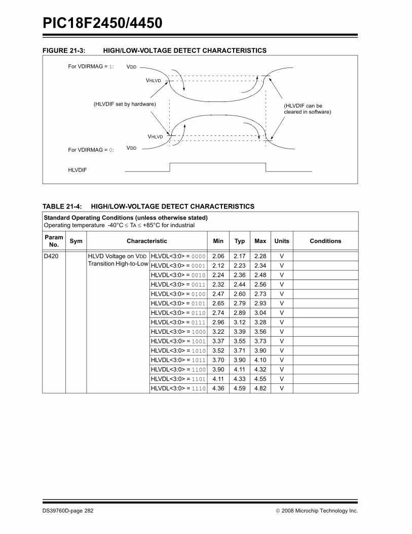
PIC18F2450/4450
DS39760D-page 282 © 2008 Microchip Technology Inc.
FIGURE 21-3: HIGH/LOW-VOLTAGE DETECT CHARACTERISTICS
TABLE 21-4: HIGH/LOW-VOLTAGE DETECT CHARACTERISTICS
VHLVD
HLVDIF
VDD
(HLVDIF set by hardware) (HLVDIF can be cleared in software)
VHLVD
For VDIRMAG = 1:
For VDIRMAG = 0: VDD
Standard Operating Conditions (unless otherwise stated)Operating temperature -40°C ≤ TA ≤ +85°C for industrial
Param No. Sym Characteristic Min Typ Max Units Conditions
D420 HLVD Voltage on VDD Transition High-to-Low
HLVDL<3:0> = 0000 2.06 2.17 2.28 VHLVDL<3:0> = 0001 2.12 2.23 2.34 VHLVDL<3:0> = 0010 2.24 2.36 2.48 VHLVDL<3:0> = 0011 2.32 2.44 2.56 VHLVDL<3:0> = 0100 2.47 2.60 2.73 VHLVDL<3:0> = 0101 2.65 2.79 2.93 VHLVDL<3:0> = 0110 2.74 2.89 3.04 VHLVDL<3:0> = 0111 2.96 3.12 3.28 VHLVDL<3:0> = 1000 3.22 3.39 3.56 VHLVDL<3:0> = 1001 3.37 3.55 3.73 VHLVDL<3:0> = 1010 3.52 3.71 3.90 VHLVDL<3:0> = 1011 3.70 3.90 4.10 VHLVDL<3:0> = 1100 3.90 4.11 4.32 VHLVDL<3:0> = 1101 4.11 4.33 4.55 VHLVDL<3:0> = 1110 4.36 4.59 4.82 V

PIC18F2450/4450
© 2008 Microchip Technology Inc. DS39760D-page 283
21.4 AC (Timing) Characteristics
21.4.1 TIMING PARAMETER SYMBOLOGYThe timing parameter symbols have been createdusing one of the following formats:
1. TppS2ppS2. TppST
F Frequency T TimeLowercase letters (pp) and their meanings:pp
mc MCLRcc CCP1 osc OSC1ck CLKO wr WRdt Data in t0 T0CKIio I/O port t1 T1CKI
:Uppercase Letters and their meaningsS
F Fall P PeriodH High R RiseI Invalid (High-Impedance) V ValidL Low Z High-Impedance
High HighLow Low

PIC18F2450/4450
DS39760D-page 284 © 2008 Microchip Technology Inc.
21.4.2 TIMING CONDITIONSThe temperature and voltages specified in Table 21-5apply to all timing specifications unless otherwisenoted. Figure 21-4 specifies the load conditions for thetiming specifications.
TABLE 21-5: TEMPERATURE AND VOLTAGE SPECIFICATIONS � AC
FIGURE 21-4: LOAD CONDITIONS FOR DEVICE TIMING SPECIFICATIONS
Note: Because of space limitations, the genericterms �PIC18FXXXX� and �PIC18LFXXXX�are used throughout this section to refer tothe PIC18F2450/4450 and PIC18LF2450/4450 families of devices specifically andonly those devices.
AC CHARACTERISTICS
Standard Operating Conditions (unless otherwise stated)Operating temperature -40°C ≤ TA ≤ +85°C for industrialOperating voltage VDD range as described in DC spec Section 21.1 and Section 21.3 . LF parts operate for industrial temperatures only.
VDD/2
CL
RL
Pin
Pin
VSS
VSS
CL
RL = 464Ω
CL = 50 pF for all pins except OSC2/CLKOand including D and E outputs as ports
Load Condition 1 Load Condition 2
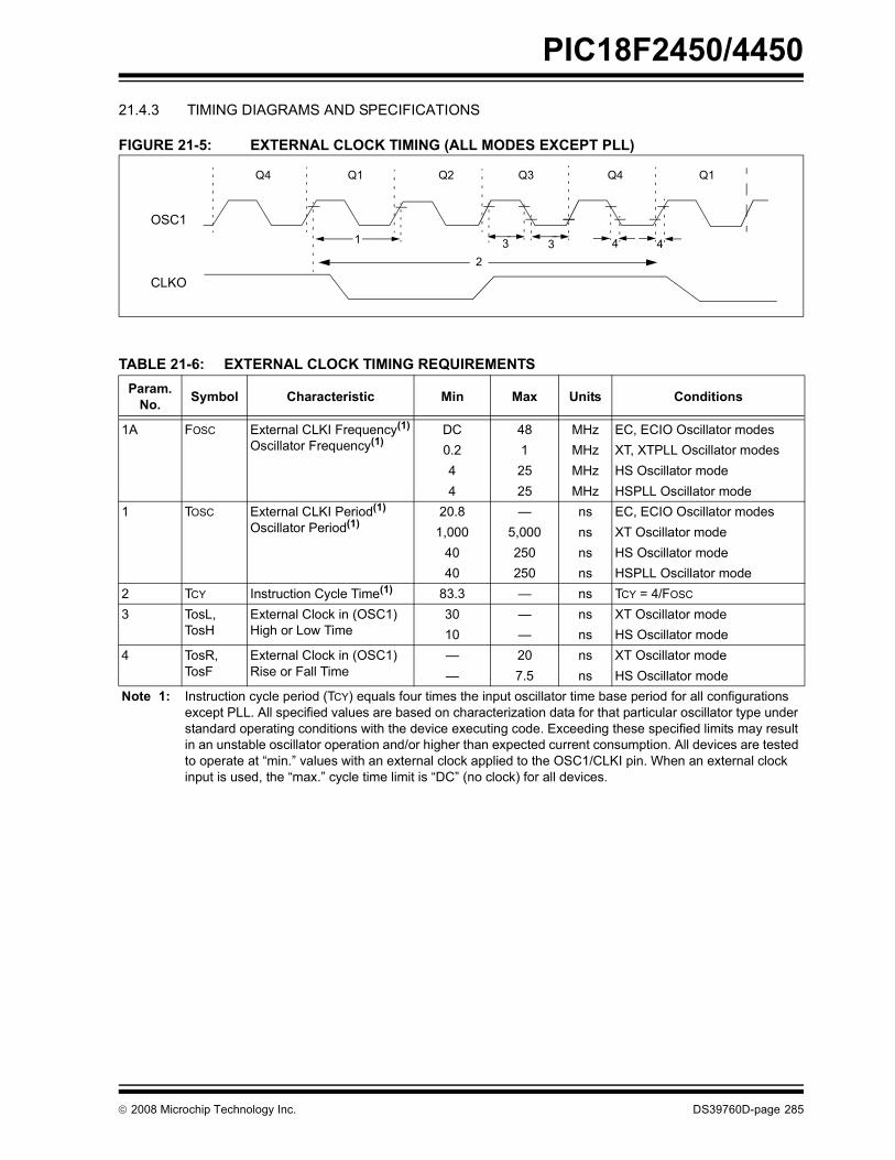
PIC18F2450/4450
© 2008 Microchip Technology Inc. DS39760D-page 285
21.4.3 TIMING DIAGRAMS AND SPECIFICATIONS
FIGURE 21-5: EXTERNAL CLOCK TIMING (ALL MODES EXCEPT PLL)
TABLE 21-6: EXTERNAL CLOCK TIMING REQUIREMENTS
OSC1
CLKO
Q4 Q1 Q2 Q3 Q4 Q1
1
23 3 4 4
Param.No. Symbol Characteristic Min Max Units Conditions
1A FOSC External CLKI Frequency(1)
Oscillator Frequency(1)DC 48 MHz EC, ECIO Oscillator modes0.2 1 MHz XT, XTPLL Oscillator modes4 25 MHz HS Oscillator mode4 25 MHz HSPLL Oscillator mode
1 TOSC External CLKI Period(1)
Oscillator Period(1)20.8 � ns EC, ECIO Oscillator modes
1,000 5,000 ns XT Oscillator mode4040
250250
nsns
HS Oscillator modeHSPLL Oscillator mode
2 TCY Instruction Cycle Time(1) 83.3 � ns TCY = 4/FOSC 3 TosL,
TosHExternal Clock in (OSC1) High or Low Time
30 � ns XT Oscillator mode10 � ns HS Oscillator mode
4 TosR,TosF
External Clock in (OSC1) Rise or Fall Time
� 20 ns XT Oscillator mode� 7.5 ns HS Oscillator mode
Note 1: Instruction cycle period (TCY) equals four times the input oscillator time base period for all configurations except PLL. All specified values are based on characterization data for that particular oscillator type under standard operating conditions with the device executing code. Exceeding these specified limits may result in an unstable oscillator operation and/or higher than expected current consumption. All devices are tested to operate at �min.� values with an external clock applied to the OSC1/CLKI pin. When an external clock input is used, the �max.� cycle time limit is �DC� (no clock) for all devices.
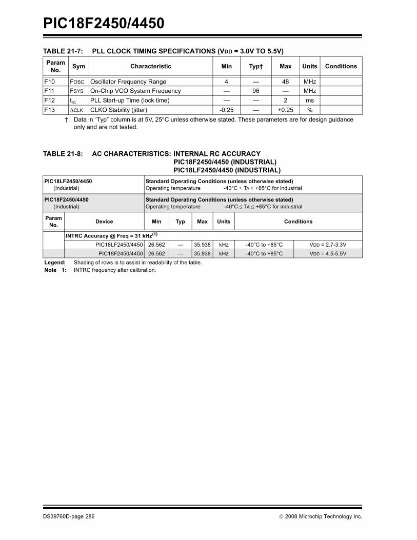
PIC18F2450/4450
DS39760D-page 286 © 2008 Microchip Technology Inc.
TABLE 21-7: PLL CLOCK TIMING SPECIFICATIONS (VDD = 3.0V TO 5.5V)
TABLE 21-8: AC CHARACTERISTICS: INTERNAL RC ACCURACYPIC18F2450/4450 (INDUSTRIAL)PIC18LF2450/4450 (INDUSTRIAL)
Param No. Sym Characteristic Min Typ� Max Units Conditions
F10 FOSC Oscillator Frequency Range 4 � 48 MHzF11 FSYS On-Chip VCO System Frequency � 96 � MHzF12 trc PLL Start-up Time (lock time) � � 2 msF13 ΔCLK CLKO Stability (jitter) -0.25 � +0.25 %
� Data in �Typ� column is at 5V, 25°C unless otherwise stated. These parameters are for design guidance only and are not tested.
PIC18LF2450/4450 (Industrial)
Standard Operating Conditions (unless otherwise stated)Operating temperature -40°C ≤ TA ≤ +85°C for industrial
PIC18F2450/4450 (Industrial)
Standard Operating Conditions (unless otherwise stated)Operating temperature -40°C ≤ TA ≤ +85°C for industrial
ParamNo. Device Min Typ Max Units Conditions
INTRC Accuracy @ Freq = 31 kHz(1)
PIC18LF2450/4450 26.562 � 35.938 kHz -40°C to +85°C VDD = 2.7-3.3VPIC18F2450/4450 26.562 � 35.938 kHz -40°C to +85°C VDD = 4.5-5.5V
Legend: Shading of rows is to assist in readability of the table.Note 1: INTRC frequency after calibration.

PIC18F2450/4450
© 2008 Microchip Technology Inc. DS39760D-page 287
FIGURE 21-6: CLKO AND I/O TIMING
TABLE 21-9: CLKO AND I/O TIMING REQUIREMENTS
Note: Refer to Figure 21-4 for load conditions.
OSC1
CLKO
I/O pin(Input)
I/O pin(Output)
Q4 Q1 Q2 Q3
10
1314
17
20, 21
19 18
15
11
12
16
Old Value New Value
ParamNo. Symbol Characteristic Min Typ Max Units Conditions
10 TosH2ckL OSC1 ↑ to CLKO ↓ � 75 200 ns (Note 1)11 TosH2ckH OSC1 ↑ to CLKO ↑ � 75 200 ns (Note 1)12 TckR CLKO Rise Time � 35 100 ns (Note 1)13 TckF CLKO Fall Time � 35 100 ns (Note 1)14 TckL2ioV CLKO ↓ to Port Out Valid � � 0.5 TCY + 20 ns (Note 1)15 TioV2ckH Port In Valid before CLKO ↑ 0.25 TCY + 25 � � ns (Note 1)16 TckH2ioI Port In Hold after CLKO ↑ 0 � � ns (Note 1)17 TosH2ioV OSC1 ↑ (Q1 cycle) to Port Out Valid � 50 150 ns18 TosH2ioI OSC1 ↑ (Q2 cycle) to
Port Input Invalid (I/O in hold time)
PIC18FXXXX 100 � � ns18A PIC18LFXXXX 200 � � ns VDD = 2.0V
19 TioV2osH Port Input Valid to OSC1 ↑ (I/O in setup time)
0 � � ns
20 TioR Port Output Rise Time PIC18FXXXX � 10 25 ns20A PIC18LFXXXX � � 60 ns VDD = 2.0V21 TioF Port Output Fall Time PIC18FXXXX � 10 25 ns21A PIC18LFXXXX � � 60 ns VDD = 2.0V22� TINP INTx Pin High or Low Time TCY � � ns23� TRBP RB7:RB4 Change Interrupt High or Low
TimeTCY � � ns
� These parameters are asynchronous events not related to any internal clock edges.Note 1: Measurements are taken in RC mode, where CLKO output is 4 x TOSC.

PIC18F2450/4450
DS39760D-page 288 © 2008 Microchip Technology Inc.
FIGURE 21-7: RESET, WATCHDOG TIMER, OSCILLATOR START-UP TIMER AND POWER-UP TIMER TIMING
FIGURE 21-8: BROWN-OUT RESET TIMING
TABLE 21-10: RESET, WATCHDOG TIMER, OSCILLATOR START-UP TIMER, POWER-UP TIMER AND BROWN-OUT RESET REQUIREMENTS
Param. No. Symbol Characteristic Min Typ Max Units Conditions
30 TmcL MCLR Pulse Width (low) 2 � � μs31 TWDT Watchdog Timer Time-out Period
(no postscaler)� 4.00 4.6 ms
32 TOST Oscillator Start-up Timer Period 1024 TOSC � 1024 TOSC � TOSC = OSC1 period33 TPWRT Power-up Timer Period � 65.5 75 ms
34 TIOZ I/O High-Impedance from MCLR Low or Watchdog Timer Reset
� 2 � μs
35 TBOR Brown-out Reset Pulse Width 200 � � μs VDD ≤ BVDD (see D005)36 TIRVST Time for Internal Reference
Voltage to become Stable� 20 50 μs
37 TLVD Low-Voltage Detect Pulse Width 200 � � μs VDD ≤ VLVD
38 TCSD CPU Start-up Time 5 � 10 μs39 TIOBST Time for INTRC to Stabilize � 1 � ms
VDD
MCLR
InternalPOR
PWRTTime-out
OscillatorTime-out
InternalReset
WatchdogTimerReset
33
32
30
3134
I/O pins
34
Note: Refer to Figure 21-4 for load conditions.
VDD BVDD
35VBGAP = 1.2V
VIRVST
Enable Internal
Internal Reference36
Reference Voltage
Voltage Stable
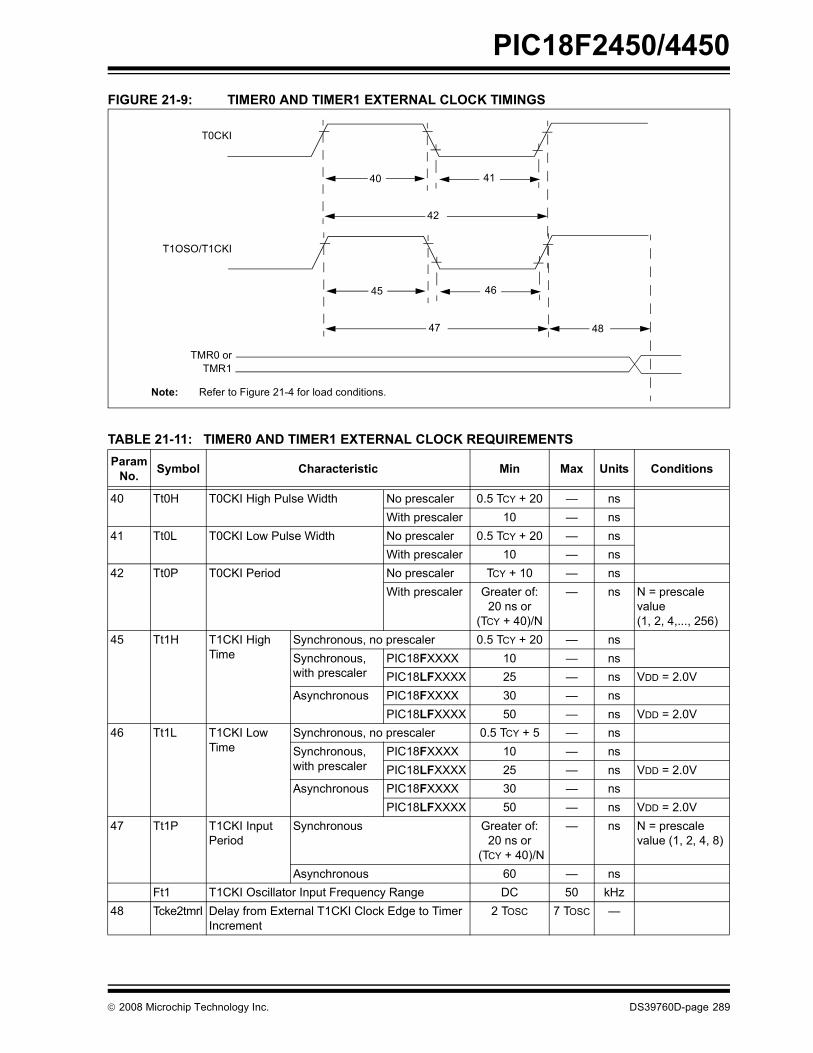
PIC18F2450/4450
© 2008 Microchip Technology Inc. DS39760D-page 289
FIGURE 21-9: TIMER0 AND TIMER1 EXTERNAL CLOCK TIMINGS
TABLE 21-11: TIMER0 AND TIMER1 EXTERNAL CLOCK REQUIREMENTS Param
No. Symbol Characteristic Min Max Units Conditions
40 Tt0H T0CKI High Pulse Width No prescaler 0.5 TCY + 20 � nsWith prescaler 10 � ns
41 Tt0L T0CKI Low Pulse Width No prescaler 0.5 TCY + 20 � nsWith prescaler 10 � ns
42 Tt0P T0CKI Period No prescaler TCY + 10 � nsWith prescaler Greater of:
20 ns or (TCY + 40)/N
� ns N = prescalevalue (1, 2, 4,..., 256)
45 Tt1H T1CKI High Time
Synchronous, no prescaler 0.5 TCY + 20 � nsSynchronous,with prescaler
PIC18FXXXX 10 � nsPIC18LFXXXX 25 � ns VDD = 2.0V
Asynchronous PIC18FXXXX 30 � nsPIC18LFXXXX 50 � ns VDD = 2.0V
46 Tt1L T1CKI Low Time
Synchronous, no prescaler 0.5 TCY + 5 � nsSynchronous, with prescaler
PIC18FXXXX 10 � nsPIC18LFXXXX 25 � ns VDD = 2.0V
Asynchronous PIC18FXXXX 30 � nsPIC18LFXXXX 50 � ns VDD = 2.0V
47 Tt1P T1CKI Input Period
Synchronous Greater of:20 ns or
(TCY + 40)/N
� ns N = prescalevalue (1, 2, 4, 8)
Asynchronous 60 � nsFt1 T1CKI Oscillator Input Frequency Range DC 50 kHz
48 Tcke2tmrI Delay from External T1CKI Clock Edge to Timer Increment
2 TOSC 7 TOSC �
Note: Refer to Figure 21-4 for load conditions.
46
47
45
48
41
42
40
T0CKI
T1OSO/T1CKI
TMR0 orTMR1
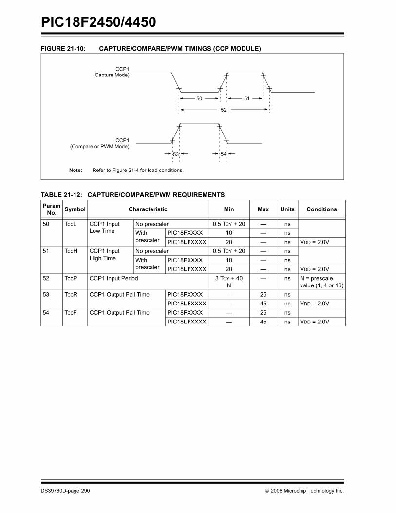
PIC18F2450/4450
DS39760D-page 290 © 2008 Microchip Technology Inc.
FIGURE 21-10: CAPTURE/COMPARE/PWM TIMINGS (CCP MODULE)
TABLE 21-12: CAPTURE/COMPARE/PWM REQUIREMENTS Param
No. Symbol Characteristic Min Max Units Conditions
50 TccL CCP1 Input Low Time
No prescaler 0.5 TCY + 20 � nsWith prescaler
PIC18FXXXX 10 � nsPIC18LFXXXX 20 � ns VDD = 2.0V
51 TccH CCP1 Input High Time
No prescaler 0.5 TCY + 20 � nsWithprescaler
PIC18FXXXX 10 � nsPIC18LFXXXX 20 � ns VDD = 2.0V
52 TccP CCP1 Input Period 3 TCY + 40N
� ns N = prescale value (1, 4 or 16)
53 TccR CCP1 Output Fall Time PIC18FXXXX � 25 nsPIC18LFXXXX � 45 ns VDD = 2.0V
54 TccF CCP1 Output Fall Time PIC18FXXXX � 25 nsPIC18LFXXXX � 45 ns VDD = 2.0V
Note: Refer to Figure 21-4 for load conditions.
CCP1(Capture Mode)
50 51
52
CCP1
53 54(Compare or PWM Mode)

PIC18F2450/4450
© 2008 Microchip Technology Inc. DS39760D-page 291
FIGURE 21-11: EUSART SYNCHRONOUS TRANSMISSION (MASTER/SLAVE) TIMING
TABLE 21-13: EUSART SYNCHRONOUS TRANSMISSION REQUIREMENTS
FIGURE 21-12: EUSART SYNCHRONOUS RECEIVE (MASTER/SLAVE) TIMING
TABLE 21-14: EUSART SYNCHRONOUS RECEIVE REQUIREMENTS
Param No. Symbol Characteristic Min Max Units Conditions
120 TckH2dtV SYNC XMIT (MASTER & SLAVE)Clock High to Data Out Valid PIC18FXXXX � 40 ns
PIC18LFXXXX � 100 ns VDD = 2.0V121 Tckrf Clock Out Rise Time and Fall Time
(Master mode)PIC18FXXXX � 20 nsPIC18LFXXXX � 50 ns VDD = 2.0V
122 Tdtrf Data Out Rise Time and Fall Time PIC18FXXXX � 20 nsPIC18LFXXXX � 50 ns VDD = 2.0V
Param. No. Symbol Characteristic Min Max Units Conditions
125 TDTV2CKL SYNC RCV (MASTER & SLAVE)Data Hold before CK ↓ (DT hold time) 10 � ns
126 TCKL2DTL Data Hold after CK ↓ (DT hold time) 15 � ns
121 121
120122
RC6/TX/CK
RC7/RX/DTpin
pin
Note: Refer to Figure 21-4 for load conditions.
125
126
RC6/TX/CK
RC7/RX/DT
pin
pin
Note: Refer to Figure 21-4 for load conditions.

PIC18F2450/4450
DS39760D-page 292 © 2008 Microchip Technology Inc.
FIGURE 21-13: USB SIGNAL TIMING
TABLE 21-15: USB LOW-SPEED TIMING REQUIREMENTS
TABLE 21-16: USB FULL-SPEED REQUIREMENTS
VCRS
USB Data Differential Lines
90%
10%
TLR, TFR TLF, TFF
Param No. Symbol Characteristic Min Typ Max Units Conditions
TLR Transition Rise Time 75 � 300 ns CL = 200 to 600 pFTLF Transition Fall Time 75 � 300 ns CL = 200 to 600 pFTLRFM Rise/Fall Time Matching 80 � 125 %
Param No. Symbol Characteristic Min Typ Max Units Conditions
TFR Transition Rise Time 4 � 20 ns CL = 50 pFTFF Transition Fall Time 4 � 20 ns CL = 50 pFTFRFM Rise/Fall Time Matching 90 � 111.1 %
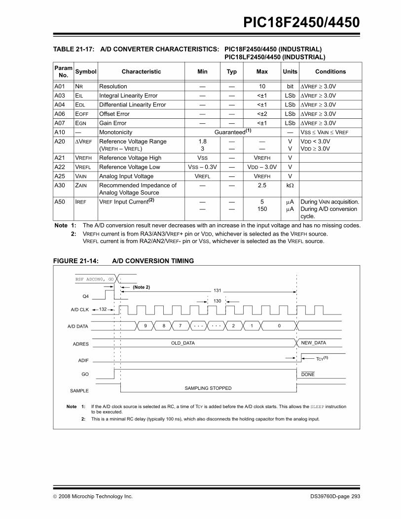
PIC18F2450/4450
© 2008 Microchip Technology Inc. DS39760D-page 293
TABLE 21-17: A/D CONVERTER CHARACTERISTICS: PIC18F2450/4450 (INDUSTRIAL) PIC18LF2450/4450 (INDUSTRIAL)
FIGURE 21-14: A/D CONVERSION TIMING
Param No. Symbol Characteristic Min Typ Max Units Conditions
A01 NR Resolution � � 10 bit ΔVREF ≥ 3.0V A03 EIL Integral Linearity Error � � <±1 LSb ΔVREF ≥ 3.0V A04 EDL Differential Linearity Error � � <±1 LSb ΔVREF ≥ 3.0V A06 EOFF Offset Error � � <±2 LSb ΔVREF ≥ 3.0VA07 EGN Gain Error � � <±1 LSb ΔVREF ≥ 3.0V A10 � Monotonicity Guaranteed(1) � VSS ≤ VAIN ≤ VREF
A20 ΔVREF Reference Voltage Range(VREFH � VREFL)
1.83
��
��
VV
VDD < 3.0VVDD ≥ 3.0V
A21 VREFH Reference Voltage High VSS � VREFH VA22 VREFL Reference Voltage Low VSS � 0.3V � VDD � 3.0V VA25 VAIN Analog Input Voltage VREFL � VREFH VA30 ZAIN Recommended Impedance of
Analog Voltage Source� � 2.5 kΩ
A50 IREF VREF Input Current(2) ��
��
5150
μAμA
During VAIN acquisition.During A/D conversion cycle.
Note 1: The A/D conversion result never decreases with an increase in the input voltage and has no missing codes.2: VREFH current is from RA3/AN3/VREF+ pin or VDD, whichever is selected as the VREFH source.
VREFL current is from RA2/AN2/VREF- pin or VSS, whichever is selected as the VREFL source.
131
130
132
BSF ADCON0, GO
Q4
A/D CLK
A/D DATA
ADRES
ADIF
GO
SAMPLE
OLD_DATA
SAMPLING STOPPED
DONE
NEW_DATA
(Note 2)
9 8 7 2 1 0
Note 1: If the A/D clock source is selected as RC, a time of TCY is added before the A/D clock starts. This allows the SLEEP instructionto be executed.
2: This is a minimal RC delay (typically 100 ns), which also disconnects the holding capacitor from the analog input.
. . . . . .
TCY(1)

PIC18F2450/4450
DS39760D-page 294 © 2008 Microchip Technology Inc.
TABLE 21-18: A/D CONVERSION REQUIREMENTS Param
No. Symbol Characteristic Min Max Units Conditions
130 TAD A/D Clock Period PIC18FXXXX 0.7 25(1) μs TOSC based, VREF ≥ 3.0VPIC18LFXXXX 1.4 25(1) μs VDD = 2.0V,
TOSC based, VREF full rangePIC18FXXXX 2.0 6.0 μs A/D RC modePIC18LFXXXX 3.0 9.0 μs VDD = 2.0V,
A/D RC mode131 TCNV Conversion Time
(not including acquisition time)(2)11 12 TAD
132 TACQ Acquisition Time(3) 1510
��
μsμs
-40°C to +85°C 0°C ≤ to ≤ +85°C
135 TSWC Switching Time from Convert → Sample � (Note 4)137 TDIS Discharge Time 0.2 � μsNote 1: The time of the A/D clock period is dependent on the device frequency and the TAD clock divider.
2: ADRES registers may be read on the following TCY cycle.3: The time for the holding capacitor to acquire the �New� input voltage when the voltage changes full scale
after the conversion (VDD to VSS or VSS to VDD). The source impedance (RS) on the input channels is 50Ω.4: On the following cycle of the device clock.

PIC18F2450/4450
© 2008 Microchip Technology Inc. DS39760D-page 295
22.0 PACKAGING INFORMATION
22.1 Package Marking Information
28-Lead SPDIP (Skinny DIP)
XXXXXXXXXXXXXXXXXXXXXXXXXXXXXXXXXX
YYWWNNN
Example
PIC18F2450-I/SP0810017
28-Lead SOIC
XXXXXXXXXXXXXXXXXXXXXXXXXXXXXXXXXXXXXXXXXXXXXXXXXXXXXXXXXXXX
YYWWNNN
Example
PIC18F2450-E/SO0810017
28-Lead QFN
XXXXXXXXXXXXXXXXYYWWNNN
Example
18F2450-I/ML0810017
3e
3e
3e
Legend: XX...X Customer-specific informationY Year code (last digit of calendar year)YY Year code (last 2 digits of calendar year)WW Week code (week of January 1 is week �01�)NNN Alphanumeric traceability code Pb-free JEDEC designator for Matte Tin (Sn)* This package is Pb-free. The Pb-free JEDEC designator ( )
can be found on the outer packaging for this package.
Note: In the event the full Microchip part number cannot be marked on one line, it willbe carried over to the next line, thus limiting the number of availablecharacters for customer-specific information.
3e
3e
PIC18F2450/4450
DS39760D-page 296 © 2008 Microchip Technology Inc.
Package Marking Information (Continued)
44-Lead TQFP
XXXXXXXXXXXXXXXXXXXXXXXXXXXXXX
YYWWNNN
Example
PIC18F4450-I/PT
0810017
XXXXXXXXXX
44-Lead QFN
XXXXXXXXXXXXXXXXXXXX
YYWWNNN
PIC18F4450
Example
-I/ML0810017
40-Lead PDIP
XXXXXXXXXXXXXXXXXXXXXXXXXXXXXXXXXXXX
XXXXXXXXXXXXXXXXXXYYWWNNN
Example
PIC18F4450-I/P0810017
3e
3e
3e

PIC18F2450/4450
© 2008 Microchip Technology Inc. DS39760D-page 297
22.2 Package DetailsThe following sections give the technical details of the packages.
��������� ������������� ��� ��������������������
!����"�� ������ �!"�����#�$�%��&"��'��� ��(�)"&�'"!&�)�����&�#�*�&����&�����&���#������� +������%����&�,����&��!&���-� ��'��!��!�����#�.��#��&�����"#��'�#�%��!����&"!��!����#�%��!����&"!��!�!������&��$���#�����/����!�#���� ��'��!��������#�&���������������.�0������
1�,2 1�!�����'��!���� ���&��������$��&� ��"��!�*��*�&�"&�&������!�
!���" 3�&���'!&��"��&����4����#�*���!(�����!��!���&��������������4�����������%���&������&�#��&��&&�255***�'��������'5���4�����
6��&! �7,8.���'��!���9�'�&! ��7 7:� ��;
7"')��%����! 7 �<��&�� � �����1�, ��&����&��������� � = = ������#�#����4���� ���4��!! �� ���� ��-� ����1�!��&����&��������� �� ���� = =��"�#��&���"�#��>�#&� . ���� �-�� �--���#�#����4����>�#&� .� ���� ��<� ����: �����9���&� � ��-�� ��-?� ����� ���&����&��������� 9 ���� ��-� ����9��#� ���4��!! � ���< ���� ����6����9��#�>�#&� )� ���� ���� ����9*��9��#�>�#&� ) ���� ���< ����: ������*����������+ �1 = = ��-�
NOTE 1
N
1 2
D
E1
eB
c
E
L
A2
eb
b1A1
A
3
������� ������� ��*��� ,������1

PIC18F2450/4450
DS39760D-page 298 © 2008 Microchip Technology Inc.
������������������#���� ��#��$���%&'(��������#�)
!����"�� ������ �!"�����#�$�%��&"��'��� ��(�)"&�'"!&�)�����&�#�*�&����&�����&���#������� +������%����&�,����&��!&���-� ��'��!��!�����#�.��#��&�����"#��'�#�%��!����&"!��!����#�%��!����&"!��!�!������&��$���#������''����!�#���� ��'��!��������#�&���������������.�0������
1�,2 1�!�����'��!���� ���&��������$��&� ��"��!�*��*�&�"&�&������!��.32 ��%��������'��!��(�"!"�����*�&�"&�&������(�%���%'�&����"�!�!�����
!���" 3�&���'!&��"��&����4����#�*���!(�����!��!���&��������������4�����������%���&������&�#��&��&&�255***�'��������'5���4�����
6��&! ��99��. .����'��!���9�'�&! ��7 7:� ��;
7"')��%����! 7 �<��&�� � �����1�,: �����8����& � = = ��?���#�#����4���� ���4��!! �� ���� = =�&��#%%��+ �� ���� = ��-�: �����>�#&� . ���-��1�,��#�#����4����>�#&� .� �����1�,: �����9���&� � ������1�,,��'%��@�&����A � ���� = ����3&�9���&� 9 ���� = ����3&���& 9� ������.33&������� � � �B = <B9��#� ���4��!! � ���< = ��--9��#�>�#&� ) ��-� = ������#���%&������� � � �B = ��B��#���%&�������1&&' � �B = ��B
c
hh
LL1
A2
A1
A
NOTE 1
1 2 3
be
EE1
D
φ
β
α
N
������� ������� ��*��� ,������1

PIC18F2450/4450
© 2008 Microchip Technology Inc. DS39760D-page 299
��������������*���+���%!����������,��-���./.�������*+! 0��1�'((��)� ������ ,�1
!����"�� ������ �!"�����#�$�%��&"��'��� ��(�)"&�'"!&�)�����&�#�*�&����&�����&���#������� ���4�����!�!�*�!���"��&�#�-� ��'��!��������#�&���������������.�0������
1�,2 1�!�����'��!���� ���&��������$��&� ��"��!�*��*�&�"&�&������!��.32 ��%��������'��!��(�"!"�����*�&�"&�&������(�%���%'�&����"�!�!�����
!���" 3�&���'!&��"��&����4����#�*���!(�����!��!���&��������������4�����������%���&������&�#��&��&&�255***�'��������'5���4�����
6��&! ��99��. .����'��!���9�'�&! ��7 7:� ��;
7"')��%����! 7 �<��&�� � ��?��1�,: �����8����& � ��<� ���� �����&��#%%� �� ���� ���� ����,�&��&� ���4��!! �- ������.3: �����>�#&� . ?����1�,.$�!�#���#�>�#&� .� -�?� -��� ����: �����9���&� � ?����1�,.$�!�#���#�9���&� �� -�?� -��� ����,�&��&�>�#&� ) ���- ��-� ��-�,�&��&�9���&� 9 ���� ���� ����,�&��&�&�.$�!�#���# C ���� = =
D EXPOSED D2
e
b
K
E2
E
L
N
NOTE 1
1
22
1
N
A
A1A3
TOP VIEW BOTTOM VIEW
PAD
������� ������� ��*��� ,������1
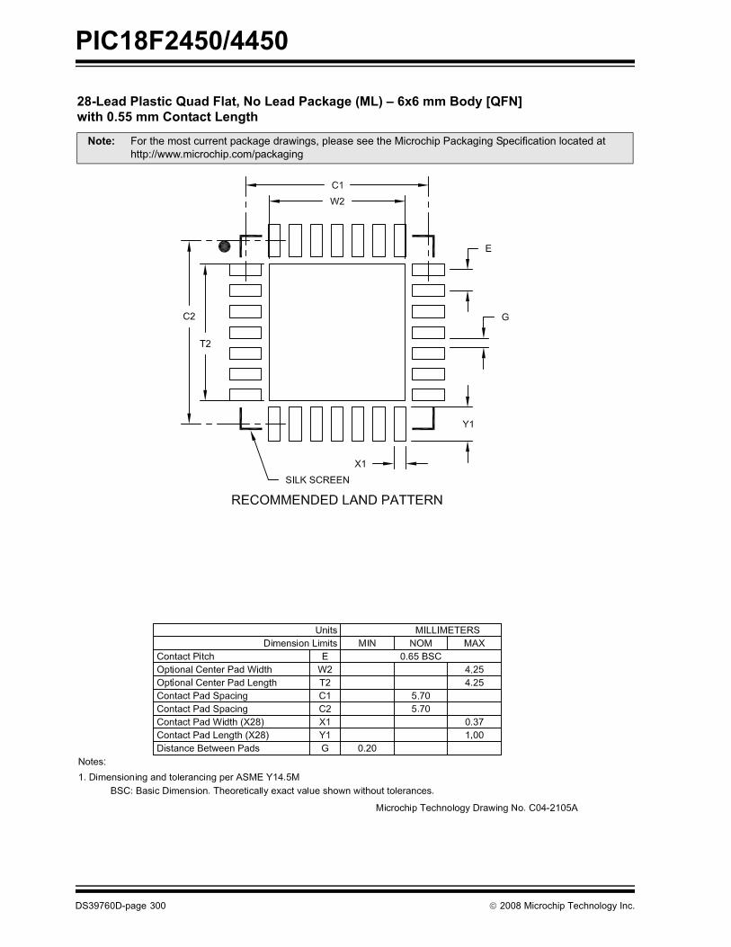
PIC18F2450/4450
DS39760D-page 300 © 2008 Microchip Technology Inc.
��������������*���+���%!����������,��-���./.�������*+! 0��1�'((��)� ������ ,�1
!���" 3�&���'!&��"��&����4����#�*���!(�����!��!���&��������������4�����������%���&������&�#��&��&&�255***�'��������'5���4�����

PIC18F2450/4450
© 2008 Microchip Technology Inc. DS39760D-page 301
2������������������ ��� �����.��������������
!����"�� ������ �!"�����#�$�%��&"��'��� ��(�)"&�'"!&�)�����&�#�*�&����&�����&���#������� +������%����&�,����&��!&���-� ��'��!��!�����#�.��#��&�����"#��'�#�%��!����&"!��!����#�%��!����&"!��!�!������&��$���#�����/����!�#���� ��'��!��������#�&���������������.�0������
1�,2 1�!�����'��!���� ���&��������$��&� ��"��!�*��*�&�"&�&������!�
!���" 3�&���'!&��"��&����4����#�*���!(�����!��!���&��������������4�����������%���&������&�#��&��&&�255***�'��������'5���4�����
6��&! �7,8.���'��!���9�'�&! ��7 7:� ��;
7"')��%����! 7 ����&�� � �����1�, ��&����&��������� � = = ������#�#����4���� ���4��!! �� ���� = ����1�!��&����&��������� �� ���� = =��"�#��&���"�#��>�#&� . ���� = �?����#�#����4����>�#&� .� ��<� = ��<�: �����9���&� � ���<� = ����� ���&����&��������� 9 ���� = ����9��#� ���4��!! � ���< = ����6����9��#�>�#&� )� ��-� = ����9*��9��#�>�#&� ) ���� = ���-: ������*����������+ �1 = = ����
N
NOTE 1
E1
D
1 2 3
A
A1b1
b e
c
eB
E
L
A2
������� ������� ��*��� ,�����?1
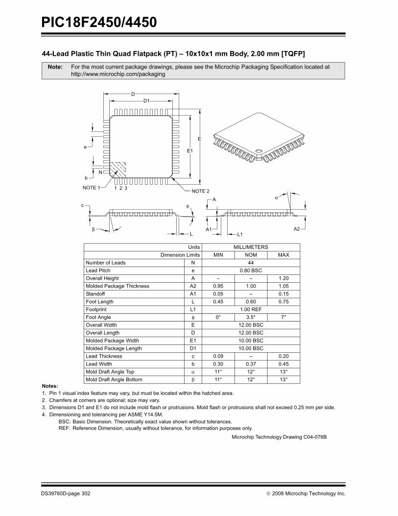
PIC18F2450/4450
DS39760D-page 302 © 2008 Microchip Technology Inc.
22������������31� *���+���4�����3��5�/5�/5������%�'�����3*+�
!����"�� ������ �!"�����#�$�%��&"��'��� ��(�)"&�'"!&�)�����&�#�*�&����&�����&���#������� ,��'%�!��&����!�����&����D�!�E��'��� ���-� ��'��!��!������#�.��#��&�����"#��'�#�%��!����&"!��!����#�%��!����&"!��!�!������&��$���#������''����!�#���� ��'��!��������#�&���������������.�0������
1�,2 1�!�����'��!���� ���&��������$��&� ��"��!�*��*�&�"&�&������!��.32 ��%��������'��!��(�"!"�����*�&�"&�&������(�%���%'�&����"�!�!�����
!���" 3�&���'!&��"��&����4����#�*���!(�����!��!���&��������������4�����������%���&������&�#��&��&&�255***�'��������'5���4�����
6��&! ��99��. .����'��!���9�'�&! ��7 7:� ��;
7"')��%�9��#! 7 ��9��#���&�� � ��<��1�,: �����8����& � = = ������#�#����4���� ���4��!! �� ���� ���� �����&��#%%�� �� ���� = ����3&�9���&� 9 ���� ��?� ����3&���& 9� ������.33&������ � �B -��B �B: �����>�#&� . ������1�,: �����9���&� � ������1�,��#�#����4����>�#&� .� ������1�,��#�#����4����9���&� �� ������1�,9��#� ���4��!! � ���� = ����9��#�>�#&� ) ��-� ��-� ������#���%&������� � � ��B ��B �-B��#���%&�������1&&' � ��B ��B �-B
A
E
E1
DD1
e
b
NOTE 1NOTE 2
N
1 2 3
c
A1L
A2L1
α
φ
β
������� ������� ��*��� ,�����?1

PIC18F2450/4450
© 2008 Microchip Technology Inc. DS39760D-page 303
22������������31� *���+���4�����3��5�/5�/5������%�'�����3*+�
!���" 3�&���'!&��"��&����4����#�*���!(�����!��!���&��������������4�����������%���&������&�#��&��&&�255***�'��������'5���4�����
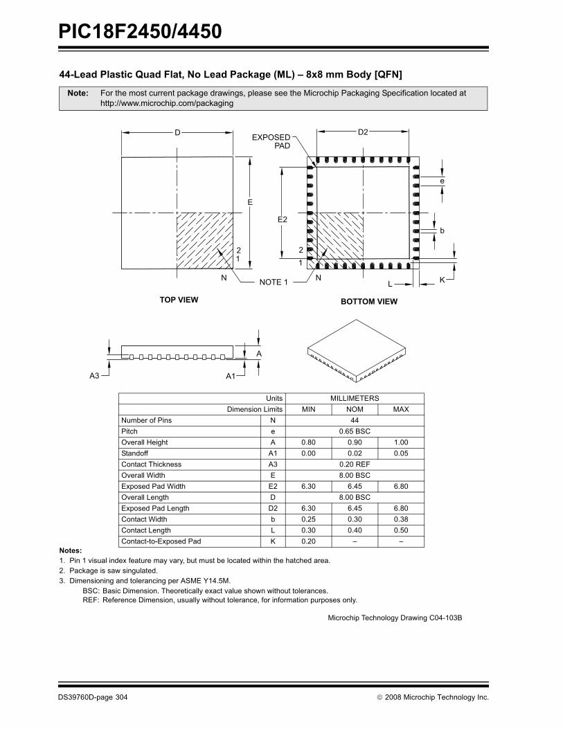
PIC18F2450/4450
DS39760D-page 304 © 2008 Microchip Technology Inc.
22������������*���+���%!����������,��-����/��������*+!
!����"�� ������ �!"�����#�$�%��&"��'��� ��(�)"&�'"!&�)�����&�#�*�&����&�����&���#������� ���4�����!�!�*�!���"��&�#�-� ��'��!��������#�&���������������.�0������
1�,2 1�!�����'��!���� ���&��������$��&� ��"��!�*��*�&�"&�&������!��.32 ��%��������'��!��(�"!"�����*�&�"&�&������(�%���%'�&����"�!�!�����
!���" 3�&���'!&��"��&����4����#�*���!(�����!��!���&��������������4�����������%���&������&�#��&��&&�255***�'��������'5���4�����
6��&! ��99��. .����'��!���9�'�&! ��7 7:� ��;
7"')��%����! 7 ����&�� � ��?��1�,: �����8����& � ��<� ���� �����&��#%%� �� ���� ���� ����,�&��&� ���4��!! �- ������.3: �����>�#&� . <����1�,.$�!�#���#�>�#&� .� ?�-� ?��� ?�<�: �����9���&� � <����1�,.$�!�#���#�9���&� �� ?�-� ?��� ?�<�,�&��&�>�#&� ) ���� ��-� ��-<,�&��&�9���&� 9 ��-� ���� ����,�&��&�&�.$�!�#���# C ���� = =
D EXPOSEDPAD
D2
e
b
KL
E2
21
NNOTE 1
21
E
N
BOTTOM VIEWTOP VIEW
A3 A1
A
������� ������� ��*��� ,�����-1

PIC18F2450/4450
© 2008 Microchip Technology Inc. DS39760D-page 305
22������������*���+���%!����������,��-����/��������*+!
!���" 3�&���'!&��"��&����4����#�*���!(�����!��!���&��������������4�����������%���&������&�#��&��&&�255***�'��������'5���4�����

PIC18F2450/4450
DS39760D-page 306 © 2008 Microchip Technology Inc.
NOTES:
PIC18F2450/4450
© 2008 Microchip Technology Inc. DS39760D-page 307
APPENDIX A: REVISION HISTORY
Revision A (January 2006)Original data sheet for PIC18F2450/4450 devices.
Revision B (January 2007)Example 11-1 and Figure 14-1 have been updated,Section 14.5.1.1 �Bus Activity Detect Interrupt Bit(ACTVIF)� and Section 14.2.2.3 �Internal Pull-upResistors� have been added, the Electrical Specifi-cations in Section 21.0 �Electrical Characteris-tics� have been updated, the package diagrams inSection 22.2 �Package Details� have been updatedand there have been minor corrections to the datasheet text.
Revision C (August 2007)The Electrical Specifications in Section 21.2 �DCCharacteristics: Power-Down and Supply Current�have been updated and the package diagrams inSection 22.2 �Package Details� have been updated.
Revision D (March 2008)Minor edits to Section 14.0 �Universal Serial Bus(USB)�, Section 16.0 �10-Bit Analog-to-DigitalConverter (A/D) Module�, Section 18.0 �SpecialFeatures of the CPU� and Section 21.0 �ElectricalCharacteristics�.

PIC18F2450/4450
DS39760D-page 308 © 2008 Microchip Technology Inc.
APPENDIX B: DEVICE DIFFERENCES
The differences between the devices listed in this datasheet are shown in Table B-1.
TABLE B-1: DEVICE DIFFERENCES Features PIC18F2450 PIC18F4450
Program Memory (Bytes) 16384 16384Program Memory (Instructions) 8192 8192Interrupt Sources 13 13I/O Ports Ports A, B, C, (E) Ports A, B, C, D, ECapture/Compare/PWM Modules 1 110-Bit Analog-to-Digital Module 10 Input Channels 13 Input ChannelsPackages 28-Pin SPDIP
28-Pin SOIC28-Pin QFN
40-Pin PDIP44-Pin TQFP44-Pin QFN

PIC18F2450/4450
© 2008 Microchip Technology Inc. DS39760D-page 309
APPENDIX C: CONVERSION CONSIDERATIONS
This appendix discusses the considerations forconverting from previous versions of a device to theones listed in this data sheet. Typically, these changesare due to the differences in the process technologyused. An example of this type of conversion is from aPIC16C74A to a PIC16C74B.
Not Applicable
APPENDIX D: MIGRATION FROM BASELINE TO ENHANCED DEVICES
This section discusses how to migrate from a Baselinedevice (i.e., PIC16C5X) to an Enhanced MCU device(i.e., PIC18FXXX).
The following are the list of modifications over thePIC16C5X microcontroller family:
Not Currently Available
PIC18F2450/4450
DS39760D-page 310 © 2008 Microchip Technology Inc.
APPENDIX E: MIGRATION FROM MID-RANGE TO ENHANCED DEVICES
A detailed discussion of the differences between theMid-Range MCU devices (i.e., PIC16CXXX) and theEnhanced devices (i.e., PIC18FXXX) is provided inAN716, �Migrating Designs from PIC16C74A/74B toPIC18C442�. The changes discussed, while devicespecific, are generally applicable to all Mid-Range toEnhanced device migrations.
This Application Note is available as Literature NumberDS00716.
APPENDIX F: MIGRATION FROM HIGH-END TO ENHANCED DEVICES
A detailed discussion of the migration pathway anddifferences between the High-End MCU devices (i.e.,PIC17CXXX) and the Enhanced devices (i.e.,PIC18FXXX) is provided in AN726, �PIC17CXXX toPIC18CXXX Migration�. This Application Note isavailable as Literature Number DS00726.
PIC18F2450/4450
© 2008 Microchip Technology Inc. DS39760D-page 311
INDEXAA/D ................................................................................... 175
Acquisition Requirements ........................................ 180ADCON0 Register .................................................... 175ADCON1 Register .................................................... 175ADCON2 Register .................................................... 175ADRESH Register ............................................ 175, 178ADRESL Register .................................................... 175Analog Port Pins, Configuring .................................. 182Associated Registers ............................................... 184Configuring the Module ............................................ 179Conversion Clock (TAD) ........................................... 181Conversion Requirements ....................................... 294Conversion Status (GO/DONE Bit) .......................... 178Conversions ............................................................. 183Converter Characteristics ........................................ 293Converter Interrupt, Configuring .............................. 179Discharge ................................................................. 183Operation in Power-Managed Modes ...................... 182Selecting and Configuring Acquisition Time ............ 181Special Event Trigger (CCP1) .................................. 184Use of the CCP1 Trigger .......................................... 184
Absolute Maximum Ratings ............................................. 267AC (Timing) Characteristics ............................................. 283
Load Conditions for Device Timing Specifications ................................................... 284
Parameter Symbology ............................................. 283Temperature and Voltage Specifications ................. 284Timing Conditions .................................................... 284
AC CharacteristicsInternal RC Accuracy ............................................... 286
ADCON0 Register ............................................................ 175GO/DONE Bit ........................................................... 178
ADCON1 Register ............................................................ 175ADCON2 Register ............................................................ 175ADDFSR .......................................................................... 256ADDLW ............................................................................ 219ADDULNK ........................................................................ 256ADDWF ............................................................................ 219ADDWFC ......................................................................... 220ADRESH Register ............................................................ 175ADRESL Register .................................................... 175, 178Analog-to-Digital Converter. See A/D.ANDLW ............................................................................ 220ANDWF ............................................................................ 221Assembler
MPASM Assembler .................................................. 264Auto-Wake-up on Sync Break Character ......................... 167
BBC .................................................................................... 221BCF .................................................................................. 222Block Diagrams
A/D ........................................................................... 178Analog Input Model .................................................. 179Capture Mode Operation ......................................... 124Compare Mode Operation ....................................... 125Device Clock .............................................................. 24EUSART Receive .................................................... 165EUSART Transmit ................................................... 163External Power-on Reset Circuit
(Slow VDD Power-up) ......................................... 43Fail-Safe Clock Monitor ............................................ 206
Generic I/O Port ......................................................... 99High/Low-Voltage Detect with External Input .......... 186Interrupt Logic ............................................................ 86On-Chip Reset Circuit ................................................ 41PIC18F2450 .............................................................. 10PIC18F4450 .............................................................. 11PLL (HS Mode) .......................................................... 26PWM Operation (Simplified) .................................... 127Reads from Flash Program Memory ......................... 77Table Read Operation ............................................... 73Table Write Operation ............................................... 74Table Writes to Flash Program Memory .................... 79Timer0 in 16-Bit Mode ............................................. 112Timer0 in 8-Bit Mode ............................................... 112Timer1 ..................................................................... 116Timer1 (16-Bit Read/Write Mode) ............................ 116Timer2 ..................................................................... 122Typical External Transceiver with Isolation ............. 131USB Interrupt Logic Funnel ..................................... 143USB Peripheral and Options ................................... 129USTAT FIFO ............................................................ 134Watchdog Timer ...................................................... 203
BN .................................................................................... 222BNC ................................................................................. 223BNN ................................................................................. 223BNOV .............................................................................. 224BNZ ................................................................................. 224BOR. See Brown-out Reset.BOV ................................................................................. 227BRA ................................................................................. 225Brown-out Reset (BOR) ..................................................... 44
Detecting ................................................................... 44Disabling in Sleep Mode ............................................ 44Software Enabled ...................................................... 44
BSF .................................................................................. 225BTFSC ............................................................................. 226BTFSS ............................................................................. 226BTG ................................................................................. 227BZ .................................................................................... 228
CC Compilers
MPLAB C18 ............................................................. 264MPLAB C30 ............................................................. 264
CALL ................................................................................ 228CALLW ............................................................................ 257Capture (CCP Module) .................................................... 124
Associated Registers ............................................... 126CCP1 Pin Configuration .......................................... 124CCPR1H:CCPR1L Registers .................................. 124Prescaler ................................................................. 124Software Interrupt .................................................... 124
Capture/Compare/PWM (CCP) ....................................... 123Capture Mode. See Capture.CCP Mode and Timer Resources ............................ 124CCPR1H Register ................................................... 124CCPR1L Register .................................................... 124Compare Mode. See Compare.Module Configuration .............................................. 124
Clock Sources .................................................................... 30Selection Using OSCCON Register .......................... 30
CLRF ............................................................................... 229CLRWDT ......................................................................... 229
PIC18F2450/4450
DS39760D-page 312 © 2008 Microchip Technology Inc.
Code Examples16 x 16 Signed Multiply Routine ................................ 8416 x 16 Unsigned Multiply Routine ............................ 848 x 8 Signed Multiply Routine .................................... 838 x 8 Unsigned Multiply Routine ................................ 83Changing Between Capture Prescalers ................... 124Computed GOTO Using an Offset Value ................... 56Erasing a Flash Program Memory Row ..................... 78Fast Register Stack .................................................... 56How to Clear RAM (Bank 1) Using
Indirect Addressing ............................................ 67Implementing a Real-Time Clock Using
a Timer1 Interrupt Service ............................... 119Initializing PORTA ...................................................... 99Initializing PORTB .................................................... 101Initializing PORTC .................................................... 104Initializing PORTD .................................................... 107Initializing PORTE .................................................... 109Reading a Flash Program Memory Word .................. 77Saving STATUS, WREG and
BSR Registers in RAM ....................................... 97Writing to Flash Program Memory ....................... 80�81
Code Protection ............................................................... 191COMF ............................................................................... 230Compare (CCP Module) ................................................... 125
Associated Registers ............................................... 126CCP1 Pin Configuration ........................................... 125CCPR1 Register ...................................................... 125Software Interrupt .................................................... 125Special Event Trigger ............................................... 125Timer1 Mode Selection ............................................ 125
Configuration Bits ............................................................. 192Configuration Register Protection .................................... 211Context Saving During Interrupts ....................................... 97Conversion Considerations .............................................. 309CPFSEQ .......................................................................... 230CPFSGT ........................................................................... 231CPFSLT ........................................................................... 231Crystal Oscillator/Ceramic Resonator ................................ 25Customer Change Notification Service ............................ 319Customer Notification Service .......................................... 319Customer Support ............................................................ 319
DData Addressing Modes ..................................................... 67
Comparing Addressing Modes with the Extended Instruction Set Enabled ................ 71
Direct .......................................................................... 67Indexed Literal Offset ................................................. 70
BSR Operation ................................................... 72Instructions Affected .......................................... 70Mapping the Access Bank ................................. 72
Indirect ....................................................................... 67Inherent and Literal .................................................... 67
Data Memory ...................................................................... 59Access Bank .............................................................. 61and the Extended Instruction Set ............................... 70Bank Select Register (BSR) ....................................... 59General Purpose Registers ........................................ 61Map for PIC18F2450/4450 Devices ........................... 60Special Function Registers ........................................ 62
Map .................................................................... 62USB RAM ................................................................... 59
DAW ................................................................................ 232DC Characteristics ........................................................... 278
Power-Down and Supply Current ............................ 270Supply Voltage ........................................................ 269
DCFSNZ .......................................................................... 233DECF ............................................................................... 232DECFSZ .......................................................................... 233Dedicated ICD/ICSP Port ................................................ 211Demonstration, Development and
Evaluation Boards ................................................... 266Development Support ...................................................... 263Device Differences ........................................................... 308Device Overview .................................................................. 7
Features (table) ........................................................... 9New Core Features ...................................................... 7Other Special Features ................................................ 8
Direct Addressing .............................................................. 68
EEffect on Standard PIC MCU
Instructions .............................................................. 260Electrical Characteristics ................................................. 267Enhanced Universal Synchronous Receiver
Transmitter (USART). See EUSART.Equations
A/D Acquisition Time ............................................... 180A/D Minimum Charging Time ................................... 180Calculating the Minimum Required
A/D Acquisition Time ....................................... 180Errata ................................................................................... 6EUSART
Asynchronous Mode ................................................ 163Associated Registers, Receive ........................ 166Associated Registers, Transmit ....................... 164Auto-Wake-up on Sync Break ......................... 167Break Character Sequence ............................. 168Receiver .......................................................... 165Receiving a Break Character ........................... 168Setting Up 9-Bit Mode with
Address Detect ........................................ 165Transmitter ...................................................... 163
Baud Rate Generator (BRG) ................................... 157Associated Registers ....................................... 158Auto-Baud Rate Detect .................................... 161Baud Rate Error, Calculating ........................... 158Baud Rates, Asynchronous Modes ................. 159High Baud Rate Select (BRGH Bit) ................. 157Operation in Power-Managed Modes .............. 157Sampling .......................................................... 157
Synchronous Master Mode ...................................... 169Associated Registers, Receive ........................ 171Associated Registers, Transmit ....................... 170Reception ........................................................ 171Transmission ................................................... 169
Synchronous Slave Mode ........................................ 172Associated Registers, Receive ........................ 173Associated Registers, Transmit ....................... 172Reception ........................................................ 173Transmission ................................................... 172
PIC18F2450/4450
© 2008 Microchip Technology Inc. DS39760D-page 313
Extended Instruction Set .................................................. 255ADDFSR .................................................................. 256ADDULNK ................................................................ 256CALLW ..................................................................... 257Considerations for Use ............................................ 260MOVSF .................................................................... 257MOVSS .................................................................... 258PUSHL ..................................................................... 258SUBFSR .................................................................. 259SUBULNK ................................................................ 259Syntax ...................................................................... 255Use with MPLAB IDE Tools ..................................... 262
External Clock Input ........................................................... 26
FFail-Safe Clock Monitor ............................................ 191, 206
Exiting Operation ..................................................... 206Interrupts in Power-Managed Modes ....................... 207POR or Wake-up From Sleep .................................. 207WDT During Oscillator Failure ................................. 206
Fast Register Stack ............................................................ 56Firmware Instructions ....................................................... 213Flash Program Memory ..................................................... 73
Associated Registers ................................................. 81Control Registers ....................................................... 74
EECON1 and EECON2 ..................................... 74TABLAT (Table Latch) Register ......................... 76TBLPTR (Table Pointer) Register ...................... 76
Erase Sequence ........................................................ 78Erasing ....................................................................... 78Operation During Code-Protect ................................. 81Protection Against Spurious Writes ........................... 81Reading ...................................................................... 77Table Pointer
Boundaries Based on Operation ........................ 76Table Pointer Boundaries .......................................... 76Table Reads and Table Writes .................................. 73Unexpected Termination of Write .............................. 81Write Sequence ......................................................... 79Write Verify ................................................................ 81Writing To ................................................................... 79
FSCM. See Fail-Safe Clock Monitor.
GGOTO .............................................................................. 234
HHardware Multiplier ............................................................ 83
Introduction ................................................................ 83Operation ................................................................... 83Performance Comparison .......................................... 83
High/Low-Voltage Detect ................................................. 185Applications .............................................................. 188Associated Registers ............................................... 189Characteristics ......................................................... 282Current Consumption ............................................... 187Effects of a Reset ..................................................... 189Operation ................................................................. 186
During Sleep .................................................... 189Setup ........................................................................ 187Start-up Time ........................................................... 187Typical Application ................................................... 188
HLVD. See High/Low-Voltage Detect.
II/O Ports ............................................................................ 99ID Locations ............................................................. 191, 211Idle Modes ......................................................................... 37INCF ................................................................................ 234INCFSZ ............................................................................ 235In-Circuit Debugger .......................................................... 211In-Circuit Serial Programming (ICSP) ...................... 191, 211Indexed Literal Offset Addressing
and Standard PIC18 Instructions ............................. 260Indexed Literal Offset Mode ............................................. 260Indirect Addressing ............................................................ 68INFSNZ ............................................................................ 235Initialization Conditions for all Registers ...................... 49�52Instruction Cycle ................................................................ 57
Clocking Scheme ....................................................... 57Flow/Pipelining .......................................................... 57
Instruction Set .................................................................. 213ADDLW .................................................................... 219ADDWF ................................................................... 219ADDWF (Indexed Literal Offset mode) .................... 261ADDWFC ................................................................. 220ANDLW .................................................................... 220ANDWF ................................................................... 221BC ............................................................................ 221BCF ......................................................................... 222BN ............................................................................ 222BNC ......................................................................... 223BNN ......................................................................... 223BNOV ...................................................................... 224BNZ ......................................................................... 224BOV ......................................................................... 227BRA ......................................................................... 225BSF .......................................................................... 225BSF (Indexed Literal Offset mode) .......................... 261BTFSC ..................................................................... 226BTFSS ..................................................................... 226BTG ......................................................................... 227BZ ............................................................................ 228CALL ........................................................................ 228CLRF ....................................................................... 229CLRWDT ................................................................. 229COMF ...................................................................... 230CPFSEQ .................................................................. 230CPFSGT .................................................................. 231CPFSLT ................................................................... 231DAW ........................................................................ 232DCFSNZ .................................................................. 233DECF ....................................................................... 232DECFSZ .................................................................. 233General Format ....................................................... 215GOTO ...................................................................... 234INCF ........................................................................ 234INCFSZ .................................................................... 235INFSNZ .................................................................... 235IORLW ..................................................................... 236IORWF ..................................................................... 236LFSR ....................................................................... 237MOVF ...................................................................... 237MOVFF .................................................................... 238MOVLB .................................................................... 238MOVLW ................................................................... 239

PIC18F2450/4450
DS39760D-page 314 © 2008 Microchip Technology Inc.
MOVWF ................................................................... 239MULLW .................................................................... 240MULWF .................................................................... 240NEGF ....................................................................... 241NOP ......................................................................... 241Opcode Field Descriptions ....................................... 214POP ......................................................................... 242PUSH ....................................................................... 242RCALL ..................................................................... 243RESET ..................................................................... 243RETFIE .................................................................... 244RETLW .................................................................... 244RETURN .................................................................. 245RLCF ........................................................................ 245RLNCF ..................................................................... 246RRCF ....................................................................... 246RRNCF .................................................................... 247SETF ........................................................................ 247SETF (Indexed Literal Offset mode) ........................ 261SLEEP ..................................................................... 248Standard Instructions ............................................... 213SUBFWB .................................................................. 248SUBLW .................................................................... 249SUBWF .................................................................... 249SUBWFB .................................................................. 250SWAPF .................................................................... 250TBLRD ..................................................................... 251TBLWT ..................................................................... 252TSTFSZ ................................................................... 253XORLW .................................................................... 253XORWF .................................................................... 254
INTCON RegisterRBIF Bit .................................................................... 101
INTCON Registers ............................................................. 87Internal Oscillator Block
INTHS, INTXT, INTCKO and INTIO Modes ............... 27Internal RC Oscillator
Use with WDT .......................................................... 203Internet Address ............................................................... 319Interrupt Sources .............................................................. 191
A/D Conversion Complete ....................................... 179Capture Complete (CCP) ......................................... 124Compare Complete (CCP) ....................................... 125Interrupt-on-Change (RB7:RB4) .............................. 101INTx Pin ..................................................................... 97PORTB, Interrupt-on-Change .................................... 97TMR0 ......................................................................... 97TMR0 Overflow ........................................................ 113TMR1 Overflow ........................................................ 115TMR2 to PR2 Match (PWM) .................................... 127
Interrupts ............................................................................ 85USB ............................................................................ 85
Interrupts, Flag BitsInterrupt-on-Change (RB7:RB4)
Flag (RBIF Bit) ................................................. 101INTOSC, INTRC. See Internal Oscillator Block.IORLW ............................................................................. 236IORWF ............................................................................. 236IPR Registers ..................................................................... 94
LLFSR ................................................................................ 237Low-Voltage ICSP Programming. See Single-Supply
ICSP Programming.
MMaster Clear Reset (MCLR) .............................................. 43Memory Organization ........................................................ 53
Data Memory ............................................................. 59Program Memory ....................................................... 53
Memory Programming Requirements .............................. 280Microchip Internet Web Site ............................................. 319Migration from Baseline to Enhanced Devices ................ 309Migration from High-End to Enhanced Devices ............... 310Migration from Mid-Range to Enhanced Devices ............ 310MOVF .............................................................................. 237MOVFF ............................................................................ 238MOVLB ............................................................................ 238MOVLW ........................................................................... 239MOVSF ............................................................................ 257MOVSS ............................................................................ 258MOVWF ........................................................................... 239MPLAB ASM30 Assembler, Linker, Librarian .................. 264MPLAB ICD 2 In-Circuit Debugger .................................. 265MPLAB ICE 2000 High-Performance
Universal In-Circuit Emulator ................................... 265MPLAB Integrated Development
Environment Software ............................................. 263MPLAB PM3 Device Programmer ................................... 265MPLAB REAL ICE In-Circuit Emulator System ............... 265MPLINK Object Linker/MPLIB Object Librarian ............... 264MULLW ............................................................................ 240MULWF ............................................................................ 240
NNEGF ............................................................................... 241NOP ................................................................................. 241
OOscillator Configuration ..................................................... 23
EC .............................................................................. 23ECIO .......................................................................... 23ECPIO ....................................................................... 23ECPLL ....................................................................... 23HS .............................................................................. 23HSPLL ....................................................................... 23INTCKO ..................................................................... 23Internal Oscillator Block ............................................. 27INTHS ........................................................................ 23INTIO ......................................................................... 23INTXT ........................................................................ 23Oscillator Modes and USB Operation ........................ 24XT .............................................................................. 23XTPLL ........................................................................ 23
Oscillator Selection .......................................................... 191Oscillator Settings for USB ................................................ 27Oscillator Start-up Timer (OST) ................................... 32, 45Oscillator Switching ........................................................... 30Oscillator Transitions ......................................................... 30Oscillator, Timer1 ............................................................. 115
PPackaging Information ..................................................... 295
Details ...................................................................... 297Marking .................................................................... 295
PICkit 2 Development Programmer ................................. 266PICSTART Plus Development Programmer .................... 266PIE Registers ..................................................................... 92
PIC18F2450/4450
© 2008 Microchip Technology Inc. DS39760D-page 315
Pin FunctionsMCLR/VPP/RE3 .................................................... 12, 16NC/ICCK/ICPGC ........................................................ 21NC/ICDT/ICPGD ........................................................ 21NC/ICPORTS ............................................................. 21NC/ICRST/ICVPP ....................................................... 21OSC1/CLKI .......................................................... 12, 16OSC2/CLKO/RA6 ................................................ 12, 16RA0/AN0 .............................................................. 13, 17RA1/AN1 .............................................................. 13, 17RA2/AN2/VREF- .................................................... 13, 17RA3/AN3/VREF+ ................................................... 13, 17RA4/T0CKI/RCV .................................................. 13, 17RA5/AN4/HLVDIN ................................................ 13, 17RB0/AN12/INT0 ................................................... 14, 18RB1/AN10/INT1 ................................................... 14, 18RB2/AN8/INT2/VMO ............................................ 14, 18RB3/AN9/VPO ..................................................... 14, 18RB4/AN11/KBI0 ................................................... 14, 18RB5/KBI1/PGM .................................................... 14, 18RB6/KBI2/PGC .................................................... 14, 18RB7/KBI3/PGD .................................................... 14, 18RC0/T1OSO/T1CKI ............................................. 15, 19RC1/T1OSI/UOE .................................................. 15, 19RC2/CCP1 ........................................................... 15, 19RC4/D-/VM ........................................................... 15, 19RC5/D+/VP .......................................................... 15, 19RC6/TX/CK .......................................................... 15, 19RC7/RX/DT .......................................................... 15, 19RD0 ............................................................................ 20RD1 ............................................................................ 20RD2 ............................................................................ 20RD3 ............................................................................ 20RD4 ............................................................................ 20RD5 ............................................................................ 20RD6 ............................................................................ 20RD7 ............................................................................ 20RE0/AN5 .................................................................... 21RE1/AN6 .................................................................... 21RE2/AN7 .................................................................... 21VDD ...................................................................... 15, 21VSS ....................................................................... 15, 21VUSB ..................................................................... 15, 21
Pinout I/O DescriptionsPIC18F2450 ............................................................... 12PIC18F4450 ............................................................... 16
PIR Registers ..................................................................... 90PLL Frequency Multiplier ................................................... 26
HSPLL, XTPLL, ECPLL and ECPIO Oscillator Modes .................................... 26
PLL Lock Time-out ............................................................. 45POP ................................................................................. 242POR. See Power-on Reset.PORTA
Associated Registers ............................................... 100I/O Summary ............................................................ 100LATA Register ............................................................ 99PORTA Register ........................................................ 99TRISA Register .......................................................... 99
PORTBAssociated Registers ............................................... 103I/O Summary ........................................................... 102LATB Register ......................................................... 101PORTB Register ...................................................... 101RB7:RB4 Interrupt-on-Change Flag
(RBIF Bit) ......................................................... 101TRISB Register ........................................................ 101
PORTCAssociated Registers ............................................... 106I/O Summary ........................................................... 105LATC Register ......................................................... 104PORTC Register ...................................................... 104TRISC Register ....................................................... 104
PORTDAssociated Registers ............................................... 108I/O Summary ........................................................... 108LATD Register ......................................................... 107PORTD Register ...................................................... 107TRISD Register ....................................................... 107
PORTEAssociated Registers ............................................... 110I/O Summary ........................................................... 110LATE Register ......................................................... 109PORTE Register ...................................................... 109TRISE Register ........................................................ 109
Postscaler, WDTAssignment (PSA Bit) .............................................. 113Rate Select (T0PS2:T0PS0 Bits) ............................. 113
Power-Managed Modes ..................................................... 33and A/D Operation ................................................... 182Clock Sources ........................................................... 33Clock Transitions and Status Indicators .................... 34Effects on Various Clock Sources ............................. 32Entering ..................................................................... 33Exiting Idle and Sleep Modes .................................... 39
by Interrupt ........................................................ 39by Reset ............................................................ 39by WDT Time-out .............................................. 39Without an Oscillator Start-up Delay ................. 40
Idle ............................................................................. 37Idle Modes
PRI_IDLE .......................................................... 38RC_IDLE ........................................................... 39SEC_IDLE ......................................................... 38
Multiple Sleep Commands ......................................... 34Run Modes ................................................................ 34
PRI_RUN ........................................................... 34RC_RUN ............................................................ 36SEC_RUN ......................................................... 34
Selecting .................................................................... 33Sleep ......................................................................... 37Summary (table) ........................................................ 33
Power-on Reset (POR) ...................................................... 43Power-up Delays ............................................................... 32Power-up Timer (PWRT) ............................................. 32, 45Prescaler, Timer0 ............................................................ 113
Assignment (PSA Bit) .............................................. 113Rate Select (T0PS2:T0PS0 Bits) ............................. 113
Prescaler, Timer2 ............................................................ 128
PIC18F2450/4450
DS39760D-page 316 © 2008 Microchip Technology Inc.
PRI_IDLE Mode ................................................................. 38PRI_RUN Mode ................................................................. 34Program Counter ................................................................ 54
PCL, PCH and PCU Registers ................................... 54PCLATH and PCLATU Registers .............................. 54
Program Memoryand the Extended Instruction Set ............................... 70Code Protection ....................................................... 209Instructions ................................................................. 58
Two-Word .......................................................... 58Interrupt Vector .......................................................... 53Look-up Tables .......................................................... 56Map and Stack (diagram) ........................................... 53Reset Vector .............................................................. 53
Program Verification and Code Protection ....................... 208Associated Registers ............................................... 208
Programming, Device Instructions ................................... 213Pulse-Width Modulation. See PWM (CCP Module).PUSH ............................................................................... 242PUSH and POP Instructions .............................................. 55PUSHL ............................................................................. 258PWM (CCP Module)
Associated Registers ............................................... 128Duty Cycle ................................................................ 127Example Frequencies/Resolutions .......................... 128Period ....................................................................... 127Setup for PWM Operation ........................................ 128TMR2 to PR2 Match ................................................ 127
QQ Clock ............................................................................ 128
RRAM. See Data Memory.RC_IDLE Mode .................................................................. 39RC_RUN Mode .................................................................. 36RCALL .............................................................................. 243RCON Register
Bit Status During Initialization .................................... 48Reader Response ............................................................ 320Register File Summary ................................................. 63�65Registers
ADCON0 (A/D Control 0) ......................................... 175ADCON1 (A/D Control 1) ......................................... 176ADCON2 (A/D Control 2) ......................................... 177BAUDCON (Baud Rate Control) .............................. 156BDnSTAT (Buffer Descriptor n Status,
CPU Mode) ...................................................... 139BDnSTAT (Buffer Descriptor n Status,
SIE Mode) ........................................................ 140CCP1CON (Capture/Compare/PWM Control) ......... 123CONFIG1H (Configuration 1 High) .......................... 194CONFIG1L (Configuration 1 Low) ............................ 193CONFIG2H (Configuration 2 High) .......................... 196CONFIG2L (Configuration 2 Low) ............................ 195CONFIG3H (Configuration 3 High) .......................... 197CONFIG4L (Configuration 4 Low) ............................ 198CONFIG5H (Configuration 5 High) .......................... 199CONFIG5L (Configuration 5 Low) ............................ 199CONFIG6H (Configuration 6 High) .......................... 200CONFIG6L (Configuration 6 Low) ............................ 200CONFIG7H (Configuration 7 High) .......................... 201CONFIG7L (Configuration 7 Low) ............................ 201DEVID1 (Device ID 1) .............................................. 202DEVID2 (Device ID 2) .............................................. 202EECON1 (Memory Control 1) .................................... 75
HLVDCON (High/Low-Voltage Detect Control) ................................................ 185
INTCON (Interrupt Control) ........................................ 87INTCON2 (Interrupt Control 2) ................................... 88INTCON3 (Interrupt Control 3) ................................... 89IPR1 (Peripheral Interrupt Priority 1) ......................... 94IPR2 (Peripheral Interrupt Priority 2) ......................... 95OSCCON (Oscillator Control) .................................... 31PIE1 (Peripheral Interrupt Enable 1) .......................... 92PIE2 (Peripheral Interrupt Enable 2) .......................... 93PIR1 (Peripheral Interrupt Request (Flag) 1) ............. 90PIR2 (Peripheral Interrupt Request (Flag) 2) ............. 91PORTE .................................................................... 109RCON (Reset Control) ......................................... 42, 96RCSTA (Receive Status and Control) ..................... 155STATUS .................................................................... 66STKPTR (Stack Pointer) ............................................ 55T0CON (Timer0 Control) ......................................... 111T1CON (Timer1 Control) ......................................... 115T2CON (Timer2 Control) ......................................... 121TXSTA (Transmit Status and Control) ..................... 154UCFG (USB Configuration) ..................................... 132UCON (USB Control) ............................................... 130UEIE (USB Error Interrupt Enable) .......................... 148UEIR (USB Error Interrupt Status) ........................... 147UEPn (USB Endpoint n Control) .............................. 135UIE (USB Interrupt Enable) ..................................... 146UIR (USB Interrupt Status) ...................................... 144USTAT (USB Status) ............................................... 134WDTCON (Watchdog Timer Control) ...................... 204
RESET ............................................................................. 243Reset State of Registers .................................................... 48Reset Timers ..................................................................... 45
Oscillator Start-up Timer (OST) ................................. 45PLL Lock Time-out ..................................................... 45Power-up Timer (PWRT) ........................................... 45
Resets ........................................................................ 41, 191Brown-out Reset (BOR) ........................................... 191Oscillator Start-up Timer (OST) ............................... 191Power-on Reset (POR) ............................................ 191Power-up Timer (PWRT) ......................................... 191
RETFIE ............................................................................ 244RETLW ............................................................................ 244RETURN .......................................................................... 245Return Address Stack ........................................................ 54
and Associated Registers .......................................... 54Return Stack Pointer (STKPTR) ........................................ 55Revision History ............................................................... 307RLCF ............................................................................... 245RLNCF ............................................................................. 246RRCF ............................................................................... 246RRNCF ............................................................................ 247
SSEC_IDLE Mode ............................................................... 38SEC_RUN Mode ................................................................ 34SETF ................................................................................ 247Single-Supply ICSP Programming ................................... 212SLEEP ............................................................................. 248Sleep
OSC1 and OSC2 Pin States ...................................... 32Sleep Mode ........................................................................ 37Software Simulator (MPLAB SIM) ................................... 264Special Event Trigger. See Compare (CCP Module).Special Features of the CPU ........................................... 191Special ICPORT Features ............................................... 211

PIC18F2450/4450
© 2008 Microchip Technology Inc. DS39760D-page 317
Stack Full/Underflow Resets .............................................. 56STATUS Register .............................................................. 66SUBFSR .......................................................................... 259SUBFWB .......................................................................... 248SUBLW ............................................................................ 249SUBULNK ........................................................................ 259SUBWF ............................................................................ 249SUBWFB .......................................................................... 250SWAPF ............................................................................ 250
TT0CON Register
PSA Bit ..................................................................... 113T0CS Bit ................................................................... 112T0PS2:T0PS0 Bits ................................................... 113T0SE Bit ................................................................... 112
Table Pointer Operations (table) ........................................ 76Table Reads/Table Writes ................................................. 56TBLRD ............................................................................. 251TBLWT ............................................................................. 252Time-out in Various Situations (table) ................................ 45Time-out Sequence ............................................................ 45Timer0 .............................................................................. 111
16-Bit Mode Timer Reads and Writes ...................... 112Associated Registers ............................................... 113Clock Source Edge Select (T0SE Bit) ...................... 112Clock Source Select (T0CS Bit) ............................... 112Operation ................................................................. 112Overflow Interrupt .................................................... 113Prescaler .................................................................. 113
Switching Assignment ...................................... 113Prescaler. See Prescaler, Timer0.
Timer1 .............................................................................. 11516-Bit Read/Write Mode ........................................... 117Associated Registers ....................................... 120, 126Interrupt .................................................................... 118Operation ................................................................. 116Oscillator .......................................................... 115, 117
Layout Considerations ..................................... 118Low-Power Option ........................................... 117Using Timer1 as a Clock Source ..................... 117
Overflow Interrupt .................................................... 115Resetting, Using a Special Event
Trigger Output (CCP) ....................................... 118TMR1H Register ...................................................... 115TMR1L Register ....................................................... 115Use as a Real-Time Clock ....................................... 118
Timer2 .............................................................................. 121Associated Registers ............................................... 122Interrupt .................................................................... 122Operation ................................................................. 121Output ...................................................................... 122PR2 Register ............................................................ 127TMR2 to PR2 Match Interrupt .................................. 127
Timing DiagramsA/D Conversion ........................................................ 293Asynchronous Reception ......................................... 166Asynchronous Transmission .................................... 164Asynchronous Transmission
(Back-to-Back) ................................................. 164Automatic Baud Rate Calculation ............................ 162Auto-Wake-up Bit (WUE) During
Normal Operation ............................................ 167Auto-Wake-up Bit (WUE) During Sleep ................... 167BRG Overflow Sequence ......................................... 162Brown-out Reset (BOR) ........................................... 288
Capture/Compare/PWM (CCP) ............................... 290CLKO and I/O .......................................................... 287Clock/Instruction Cycle .............................................. 57EUSART Synchronous Receive
(Master/Slave) ................................................. 291EUSART Synchronous Transmission
(Master/Slave) ................................................. 291External Clock (All Modes Except PLL) ................... 285Fail-Safe Clock Monitor ........................................... 207High/Low-Voltage Detect Characteristics ................ 282High-Voltage Detect (VDIRMAG = 1) ...................... 188Low-Voltage Detect (VDIRMAG = 0) ....................... 187PWM Output ............................................................ 127Reset, Watchdog Timer (WDT), Oscillator
Start-up Timer (OST) and Power-up Timer (PWRT) ................................................. 288
Send Break Character Sequence ............................ 168Slow Rise Time (MCLR Tied to VDD,
VDD Rise > TPWRT) ............................................ 47Synchronous Reception
(Master Mode, SREN) ..................................... 171Synchronous Transmission ..................................... 169Synchronous Transmission (Through TXEN) .......... 170Time-out Sequence on POR w/PLL Enabled
(MCLR Tied to VDD) .......................................... 47Time-out Sequence on Power-up
(MCLR Not Tied to VDD), Case 1 ...................... 46Time-out Sequence on Power-up
(MCLR Not Tied to VDD), Case 2 ...................... 46Time-out Sequence on Power-up
(MCLR Tied to VDD, VDD Rise TPWRT) .............. 46Timer0 and Timer1 External Clock .......................... 289Transition for Entry to Idle Mode ............................... 38Transition for Entry to SEC_RUN Mode .................... 35Transition for Entry to Sleep Mode ............................ 37Transition for Two-Speed Start-up
(INTRC to HSPLL) ........................................... 205Transition for Wake From Idle to Run Mode .............. 38Transition for Wake From Sleep (HSPLL) ................. 37Transition From RC_RUN Mode to
PRI_RUN Mode ................................................. 36Transition From SEC_RUN Mode to
PRI_RUN Mode (HSPLL) .................................. 35Transition to RC_RUN Mode ..................................... 36USB Signal .............................................................. 292
Timing Diagrams and Specifications ............................... 285Capture/Compare/PWM
Requirements (CCP) ....................................... 290CLKO and I/O Requirements ................................... 287EUSART Synchronous Receive
Requirements .................................................. 291EUSART Synchronous Transmission
Requirements .................................................. 291External Clock Requirements .................................. 285PLL Clock ................................................................ 286Reset, Watchdog Timer, Oscillator Start-up
Timer, Power-up Timer and Brown-out Reset Requirements ........................................ 288
Timer0 and Timer1 External Clock Requirements .................................................. 289
USB Full-Speed Requirements ............................... 292USB Low-Speed Requirements ............................... 292
Top-of-Stack Access .......................................................... 54TQFP Packages and Special Features ........................... 211TSTFSZ ........................................................................... 253

PIC18F2450/4450
DS39760D-page 318 © 2008 Microchip Technology Inc.
Two-Speed Start-up ................................................. 191, 205Two-Word Instructions
Example Cases .......................................................... 58TXSTA Register
BRGH Bit ................................................................. 157
UUniversal Serial Bus ........................................................... 59
Address Register (UADDR) ..................................... 136Associated Registers ............................................... 150Buffer Descriptor Table ............................................ 137Buffer Descriptors .................................................... 137
Address Validation ........................................... 140Assignment in Different
Buffering Modes ....................................... 142BDnSTAT Register (CPU Mode) ..................... 138BDnSTAT Register (SIE Mode) ....................... 140Byte Count ....................................................... 140Example ........................................................... 137Memory Map .................................................... 141Ownership ........................................................ 137Ping-Pong Buffering ......................................... 141Register Summary ........................................... 142Status and Configuration ................................. 137
Class Specifications and Drivers ............................. 152Descriptors ............................................................... 152Endpoint Control ...................................................... 135Enumeration ............................................................. 152External Transceiver ................................................ 131Eye Pattern Test Enable .......................................... 133Firmware and Drivers ............................................... 150Frame Number Registers ......................................... 136Frames ..................................................................... 151Internal Transceiver ................................................. 131Internal Voltage Regulator ....................................... 133Interrupts .................................................................. 143
and USB Transactions ..................................... 143
Layered Framework ................................................. 151Oscillator Requirements .......................................... 150Output Enable Monitor ............................................. 133Overview .......................................................... 129, 151Ping-Pong Buffer Configuration ............................... 133Power ...................................................................... 151Power Modes ........................................................... 149
Bus Power Only ............................................... 149Dual Power with Self-Power
Dominance .............................................. 149Self-Power Only ............................................... 149
Pull-up Resistors ...................................................... 133RAM ......................................................................... 136
Memory Map .................................................... 136Speed ...................................................................... 152Status and Control ................................................... 130Status Register (USTAT) ......................................... 134Transfer Types ......................................................... 151UFRMH:UFRML Registers ...................................... 136
USBInternal Voltage Regulator Specifications ................ 281Module Specifications .............................................. 281
USB. See Universal Serial Bus.
WWatchdog Timer (WDT) ........................................... 191, 203
Associated Registers ............................................... 204Control Register ....................................................... 203During Oscillator Failure .......................................... 206Programming Considerations .................................. 203
WWW Address ................................................................ 319WWW, On-Line Support ...................................................... 6
XXORLW ............................................................................ 253XORWF ........................................................................... 254

© 2008 Microchip Technology Inc. DS39760D-page 319
PIC18F2450/4450
THE MICROCHIP WEB SITEMicrochip provides online support via our WWW site atwww.microchip.com. This web site is used as a meansto make files and information easily available tocustomers. Accessible by using your favorite Internetbrowser, the web site contains the followinginformation:
� Product Support � Data sheets and errata, application notes and sample programs, design resources, user�s guides and hardware support documents, latest software releases and archived software
� General Technical Support � Frequently Asked Questions (FAQ), technical support requests, online discussion groups, Microchip consultant program member listing
� Business of Microchip � Product selector and ordering guides, latest Microchip press releases, listing of seminars and events, listings of Microchip sales offices, distributors and factory representatives
CUSTOMER CHANGE NOTIFICATION SERVICEMicrochip�s customer notification service helps keepcustomers current on Microchip products. Subscriberswill receive e-mail notification whenever there arechanges, updates, revisions or errata related to aspecified product family or development tool of interest.
To register, access the Microchip web site atwww.microchip.com, click on Customer ChangeNotification and follow the registration instructions.
CUSTOMER SUPPORTUsers of Microchip products can receive assistancethrough several channels:
� Distributor or Representative� Local Sales Office� Field Application Engineer (FAE)� Technical Support� Development Systems Information Line
Customers should contact their distributor,representative or field application engineer (FAE) forsupport. Local sales offices are also available to helpcustomers. A listing of sales offices and locations isincluded in the back of this document.
Technical support is available through the web siteat: http://support.microchip.com

PIC18F2450/4450
DS39760D-page 320 © 2008 Microchip Technology Inc.
READER RESPONSEIt is our intention to provide you with the best documentation possible to ensure successful use of your Microchip prod-uct. If you wish to provide your comments on organization, clarity, subject matter, and ways in which our documentationcan better serve you, please FAX your comments to the Technical Publications Manager at (480) 792-4150.
Please list the following information, and use this outline to provide us with your comments about this document.
To: Technical Publications Manager
RE: Reader ResponseTotal Pages Sent ________
From: Name
CompanyAddressCity / State / ZIP / Country
Telephone: (_______) _________ - _________
Application (optional):
Would you like a reply? Y N
Device: Literature Number:
Questions:
FAX: (______) _________ - _________
DS39760DPIC18F2450/4450
1. What are the best features of this document?
2. How does this document meet your hardware and software development needs?
3. Do you find the organization of this document easy to follow? If not, why?
4. What additions to the document do you think would enhance the structure and subject?
5. What deletions from the document could be made without affecting the overall usefulness?
6. Is there any incorrect or misleading information (what and where)?
7. How would you improve this document?
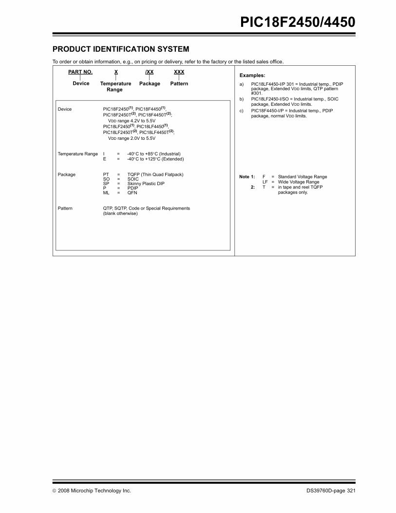
PIC18F2450/4450
© 2008 Microchip Technology Inc. DS39760D-page 321
PRODUCT IDENTIFICATION SYSTEMTo order or obtain information, e.g., on pricing or delivery, refer to the factory or the listed sales office.
PART NO. X /XX XXX
PatternPackageTemperatureRange
Device
Device PIC18F2450(1), PIC18F4450(1),
PIC18F2450T(2), PIC18F4450T(2); VDD range 4.2V to 5.5VPIC18LF2450(1), PIC18LF4450(1), PIC18LF2450T(2), PIC18LF4450T(2); VDD range 2.0V to 5.5V
Temperature Range I = -40°C to +85°C (Industrial)E = -40°C to +125°C (Extended)
Package PT = TQFP (Thin Quad Flatpack)SO = SOICSP = Skinny Plastic DIPP = PDIPML = QFN
Pattern QTP, SQTP, Code or Special Requirements (blank otherwise)
Examples:a) PIC18LF4450-I/P 301 = Industrial temp., PDIP
package, Extended VDD limits, QTP pattern #301.
b) PIC18LF2450-I/SO = Industrial temp., SOIC package, Extended VDD limits.
c) PIC18F4450-I/P = Industrial temp., PDIP package, normal VDD limits.
Note 1: F = Standard Voltage RangeLF = Wide Voltage Range
2: T = in tape and reel TQFP packages only.

DS39760D-page 322 © 2008 Microchip Technology Inc.
AMERICASCorporate Office2355 West Chandler Blvd.Chandler, AZ 85224-6199Tel: 480-792-7200 Fax: 480-792-7277Technical Support: http://support.microchip.comWeb Address: www.microchip.comAtlantaDuluth, GA Tel: 678-957-9614 Fax: 678-957-1455BostonWestborough, MA Tel: 774-760-0087 Fax: 774-760-0088ChicagoItasca, IL Tel: 630-285-0071 Fax: 630-285-0075DallasAddison, TX Tel: 972-818-7423 Fax: 972-818-2924DetroitFarmington Hills, MI Tel: 248-538-2250Fax: 248-538-2260KokomoKokomo, IN Tel: 765-864-8360Fax: 765-864-8387Los AngelesMission Viejo, CA Tel: 949-462-9523 Fax: 949-462-9608Santa ClaraSanta Clara, CA Tel: 408-961-6444Fax: 408-961-6445TorontoMississauga, Ontario, CanadaTel: 905-673-0699 Fax: 905-673-6509
ASIA/PACIFICAsia Pacific OfficeSuites 3707-14, 37th FloorTower 6, The GatewayHarbour City, KowloonHong KongTel: 852-2401-1200Fax: 852-2401-3431Australia - SydneyTel: 61-2-9868-6733Fax: 61-2-9868-6755China - BeijingTel: 86-10-8528-2100 Fax: 86-10-8528-2104China - ChengduTel: 86-28-8665-5511Fax: 86-28-8665-7889China - Hong Kong SARTel: 852-2401-1200 Fax: 852-2401-3431China - NanjingTel: 86-25-8473-2460Fax: 86-25-8473-2470China - QingdaoTel: 86-532-8502-7355Fax: 86-532-8502-7205China - ShanghaiTel: 86-21-5407-5533 Fax: 86-21-5407-5066China - ShenyangTel: 86-24-2334-2829Fax: 86-24-2334-2393China - ShenzhenTel: 86-755-8203-2660 Fax: 86-755-8203-1760China - WuhanTel: 86-27-5980-5300Fax: 86-27-5980-5118China - XiamenTel: 86-592-2388138 Fax: 86-592-2388130China - XianTel: 86-29-8833-7252Fax: 86-29-8833-7256China - ZhuhaiTel: 86-756-3210040 Fax: 86-756-3210049
ASIA/PACIFICIndia - BangaloreTel: 91-80-4182-8400 Fax: 91-80-4182-8422India - New DelhiTel: 91-11-4160-8631Fax: 91-11-4160-8632India - PuneTel: 91-20-2566-1512Fax: 91-20-2566-1513Japan - YokohamaTel: 81-45-471- 6166 Fax: 81-45-471-6122Korea - DaeguTel: 82-53-744-4301Fax: 82-53-744-4302Korea - SeoulTel: 82-2-554-7200Fax: 82-2-558-5932 or 82-2-558-5934Malaysia - Kuala LumpurTel: 60-3-6201-9857Fax: 60-3-6201-9859Malaysia - PenangTel: 60-4-227-8870Fax: 60-4-227-4068Philippines - ManilaTel: 63-2-634-9065Fax: 63-2-634-9069SingaporeTel: 65-6334-8870Fax: 65-6334-8850Taiwan - Hsin ChuTel: 886-3-572-9526Fax: 886-3-572-6459Taiwan - KaohsiungTel: 886-7-536-4818Fax: 886-7-536-4803Taiwan - TaipeiTel: 886-2-2500-6610 Fax: 886-2-2508-0102Thailand - BangkokTel: 66-2-694-1351Fax: 66-2-694-1350
EUROPEAustria - WelsTel: 43-7242-2244-39Fax: 43-7242-2244-393Denmark - CopenhagenTel: 45-4450-2828 Fax: 45-4485-2829France - ParisTel: 33-1-69-53-63-20 Fax: 33-1-69-30-90-79Germany - MunichTel: 49-89-627-144-0 Fax: 49-89-627-144-44Italy - Milan Tel: 39-0331-742611 Fax: 39-0331-466781Netherlands - DrunenTel: 31-416-690399 Fax: 31-416-690340Spain - MadridTel: 34-91-708-08-90Fax: 34-91-708-08-91UK - WokinghamTel: 44-118-921-5869Fax: 44-118-921-5820
WORLDWIDE SALES AND SERVICE
01/02/08