Embed Size (px)
Citation preview
Aula 2 - Indrotução à eletrônica digital
Prof. Renan Sebem
Disciplina de Eletrônica DigitalGraduação em Engenharia Elétrica
Universidade do Estado de Santa CatarinaJoinville-SC – Brasil
25 de fevereiro de 2016
ELD0001 ‡ Prof. Renan Sebem ‡ Aula 2 1 / 35
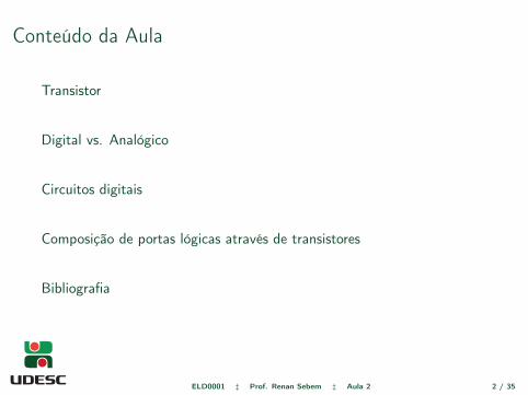
Conteúdo da Aula
Transistor
Digital vs. Analógico
Circuitos digitais
Composição de portas lógicas através de transistores
Bibliografia
ELD0001 ‡ Prof. Renan Sebem ‡ Aula 2 2 / 35
Complementando...Disciplina optativa:EL1DLP1 - DISPOSITIVOS DE LÓGICA PROGRAMÁVEL
ELD0001 ‡ Prof. Renan Sebem ‡ Aula 2 3 / 35
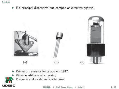
Transistor
I É o principal dispositivo que compõe os circuitos digitais.2 CHAPTER 1 Introduction
Despite the large acclaim of the transistor invention, which led the three authors to eventually share the Nobel Prize in Physics in 1956, Shockley was very dissatisfi ed with Bell Laboratories (among other reasons because his name was not included in the transistor patent because the fi nal experiment was conducted without his participation). So he eventually left to start his own company, initially intending to mass produce low-cost transistors.
The birth of silicon valley (or “Had Shockley gone elsewhere . . .“)The most common material used in electronic devices is Si (silicon), followed by GaAs (gallium arsenide), Ge (germanium), and others (all used much less frequently than Si). However, in their original form, these materials are of very little interest. What makes them useful is a process called doping, which consists of adding an impurity (called dopant) to them that creates either free electrons or free holes (the latter means a “space” where an electron is missing; the space does not have a fi xed position, causing it to be controlled by an external electrical fi eld that results in an electric current). Depending on whether the dopant generates free electrons (negative charges) or free holes (positive charges), the doped semiconductor is classifi ed as n-type or p-type, respectively. For Si, popular n-type dopants are P (phosphorous) and As (arsenic), while p-type dopants include B (boron) and Al (aluminum).
The point-contact approach used in the fi rst transistor was not adequate for mass production, so Shockley diligently searched for another approach, eventually leading to a very thin region (base) of type n (or p) sandwiched between two other regions (emitter and collector) of type p (or n). Because of its two-junction construction, this type of transistor is called BJT (bipolar junction transistor).
Shockley did his undergraduate studies at the California Institute of Technology and earned his PhD at MIT. In 1955 he returned to the West Coast to set up his company, Shockley Semiconductor, in Moun-tain View, California, which is south of San Francisco.
The subsequent events are nicely described by Gordon Moore in a speech he gave at the ground-breaking ceremony for the new engineering building at Caltech in 1994 ([Moore94], available at the Caltech Archives; also available at http://nobelprize.org under the title “The Accidental Entrepre-neur”). Very briefl y, the events are as follows. Because of Shockley’s diffi cult personality, eight of his employees, including Gordon Moore and Robert Noyce, decided to leave Shockley Semiconductor in 1957 and start a new company, called Fairchild Semiconductor, with a little capital of their own and the bulk of the fi nancing from Fairchild Camera, an East Coast corporation. The new company, like many other spin-offs that followed, established itself in the same region as Shockley’s company. Fairchild
FIGURE 1.1. (a) The fi rst transistor (1947); (b) A popular commercial encasing (called TO-92); (c) A vacuum tube.I Primeiro transistor foi criado em 1947;I Válvulas utilizam alta tensão;I Porque é melhor diminuir a tensão?
ELD0001 ‡ Prof. Renan Sebem ‡ Aula 2 4 / 35
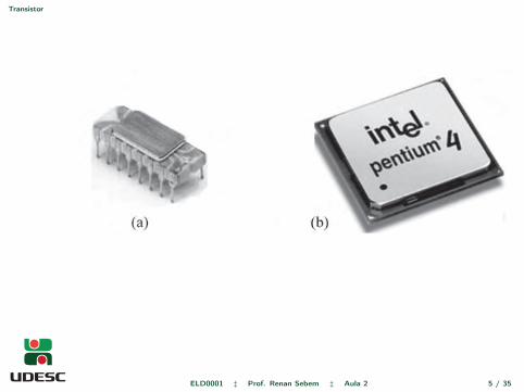
Transistor
Semiconductor turned out to be a very successful enterprise with nearly 30,000 employees after a little over 10 years. However, due to management problems and other confl icts between the West Coast (Fairchild Semiconductor) and East Coast (Fairchild Camera) operations, in 1968 Moore and Noyce left and founded their own company, Intel.
One of Intel’s fi rst great achievements was the development of MOS transistors with polysilicon gates instead of metal gates, a technology that took several years for other companies to catch up with. The fi rst integrated microprocessor, called 4004 and delivered in 1971, was also developed by Intel (see Figure 1.2(a)). It was a 4-bit processor with nearly 2300 transistors that was capable of addressing 9.2 k of external memory, employed mainly in calculators. Even though Intel’s major business in the 1980s was the fabrication of SRAM and DRAM memories, its turning point was the advent of personal computers, for which Intel still manufactures most of the microprocessors (like that shown in Figure 1.2(b)).
Even though the development of the fi rst integrated circuit in 1958 is credited to Robert Noyce (while still at Fairchild) and Jack Kilby (working independently at Texas Instruments), the 2000 Nobel Prize in Physics for that development was awarded only to the latter.
In summary, many spin-offs occurred after Shockley fi rst decided to establish his short-lived com-pany south of San Francisco (Shockley went on to become a professor at Stanford University). Because most of these companies dealt with silicon or silicon-related technologies, the area was coined “Silicon Valley” by a journalist in 1971, a nickname that rapidly became well known worldwide. So, one might wonder, “Had Shockley decided to go elsewhere . . .”
But not only of memories and microprocessors is electronics made. There are many other companies that specialize in all sorts of electronic devices. For example, some specialize in analog devices, from basic applications (operational amplifi ers, voltage regulators, etc.) to very advanced ones (wireless links, medical implants and instrumentation, satellite communication transceivers, etc.). There are also compa-nies that act in quite different parts of the digital fi eld, like those that manufacture PLDs (programmable logic devices), which constitute a fast-growing segment for the implementation of complex systems. As a result, chips containing whole systems and millions of transistors are now commonplace.
Indeed, today’s electronic complexity is so vast that probably no company or segment can claim that it is the most important or the most crucial because none can cover alone even a fraction of what is being done. Moreover, companies are now spread all over the world, so the actual contributions come from all kinds of places, people, and cultures. In fact, of all aspects that characterize modern electronic technologies, this worldwide congregation of people and cultures is probably what best represents its beauty.
FIGURE 1.2. (a) Intel 4004, the fi rst microprocessor (1971, 10 !m nMOS technology, ~2300 transistors, 108 kHz); (b) Pentium 4 microprocessor (2006, 90 nm CMOS technology, > 3 GHz, 180 million transistors). (Reprinted with permission of Intel.)
1.1 Historical Notes 3
ELD0001 ‡ Prof. Renan Sebem ‡ Aula 2 5 / 35
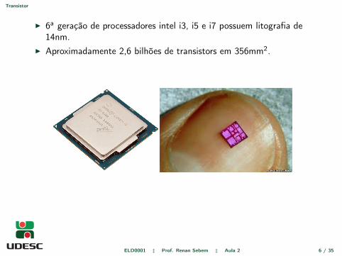
Transistor
I 6a geração de processadores intel i3, i5 e i7 possuem litografia de14nm.
I Aproximadamente 2,6 bilhões de transistors em 356mm2.
ELD0001 ‡ Prof. Renan Sebem ‡ Aula 2 6 / 35
Digital vs. Analógico
4 CHAPTER 1 Introduction
1.2 Analog versus DigitalElectronic circuits can be divided into two large groups called analog and digital. The fi rst deals with continuous-valued signals while the second concerns discrete-valued signals. Roughly speaking, the former deals with real numbers while the latter deals with integers.
Many quantities are continuous by nature, like temperature, sound intensity, and time. Others are inherently discrete, like a game’s score, the day of the month, or a corporation’s profi t. Another example is a light switch, which has only two discrete states (digital) versus a light dimmer, which has innumerous continuous states (analog).
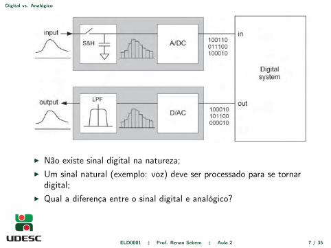
From a computational point of view, however, any signal can be treated as digital. This is made pos-sible by a circuit called analog- to-digital converter (A/DC), which converts the analog signal into digital, and by its counterpart, the digital-to-analog converter (D/AC), which reconverts the signal to its original analog form when necessary.
This process is illustrated in Figure 1.3. A sample and hold (S&H) circuit periodically samples the incoming signal, providing static values for the A/DC, which quantizes and represents them by means of bits (bits and bytes will be defi ned in the next section). At the output of the digital system, binary val-ues are delivered to the D/AC, which converts them into analog but discontinuous values, thus requiring a low-pass fi lter (LPF) to remove the high frequency components, thus “rounding” the signal’s corners and returning it approximately to its original form.
To illustrate the importance of this method, consider the recording and playing of music. The music captured by the microphones in a recording studio is analog and must be delivered in analog form to the human ear. However, in digital form, storage is easier, cheaper, and more versatile. Moreover, the music can be processed (fi ltered, mixed, superimposed, etc.) in so many ways that would be simply impossible otherwise. For those reasons, the captured sound is immediately converted from analog to digital by the A/DC, then processed, and fi nally recorded on a CD. The CD player does the opposite, that is, it reads the digital information from the CD, processes it, then passes it through the D/AC circuit, and fi nally amplifi es the analog (reconstituted) signal for proper loudspeaker reproduction.
Even though the introduction of quantization errors in the conversion/deconversion process described above is inevitable, it is still viable because a large enough number of bits can be employed in it so that the resulting error becomes too small to be perceived or too small to be relevant. As an example, let us say that the analog signal to be converted ranges from 0 V to 1 V and that 8 bits are used to encode it. In this case, 28 = 256 discrete values are allowed, so the analog signal can be divided into 256 intervals of
FIGURE 1.3. Interface between a digital system and the analog world.I Não existe sinal digital na natureza;I Um sinal natural (exemplo: voz) deve ser processado para se tornar
digital;I Qual a diferença entre o sinal digital e analógico?
ELD0001 ‡ Prof. Renan Sebem ‡ Aula 2 7 / 35
Digital vs. Analógico
Codificação binária
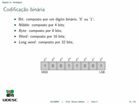
I Bit: composto por um dígito binário, ’0’ ou ’1’;I Nibble: composto por 4 bits;I Byte: composto por 8 bits;I Word : composto por 16 bits;I Long word : composto por 32 bits;
3.9 mV each (because 1 V/256 = 3.9 mV) with a binary word used to represent each interval. One option for the encoding would then be (0 V to 3.9 mV) = "00000000", (3.9 mV to 7.8 mV) = "00000001", . . ., (996.1 mV to 1 V) = "11111111". More bits can be used, and other encoding schemes also exist, like the use of nonuni-form intervals, so the maximum error can be tailored to meet specifi c applications. In standard digital music for CDs, for example, 16 bits are employed in each channel.
Another important aspect in analog/digital (A/D) conversion is the sampling rate, which is the num-ber of times the incoming signal is sampled per second (see the S&H stage in Figure 1.3). The Nyquist theorem determines that it has to be greater than twice the signal’s largest frequency. In the case of stan-dard digital music, the rate is 44.1 ksamples/s, which therefore allows the capture of signals over 20 kHz. This is enough because the human ear can detect audio signals from 50 Hz to approximately 20 kHz.
1.3 Bits, Bytes, and WordsEven though multilevel logic has been investigated for a long time, two-level logic (called binary) is still more feasible. Each component is called a bit, and its two possible values are represented by '0' and '1'. Even though the actual (physical) signals that correspond to '0' and '1' are of fundamental importance to the technology developers, they are irrelevant to the system users (to a programmer, for example).
While a single '0' or '1' is called a bit, a group of 4 bits is called a nibble, a group of 8 bits is called a byte, a group of 16 bits is called a word, and a group of 32 bits is called a long word. In the VHDL language (Chapters 19–24), the syntax is that a single bit has a pair of single quotation marks around it, such as '0' or '1', while a group of bits (called a bit vector) has a pair of double quotation marks, such as "00010011". This syntax will be adopted in the entire text.
The leftmost bit of a bit vector is normally referred to as the most signifi cant bit (MSB), while the rightmost one is called least signifi cant bit (LSB). The reason for such designations can be observed in Figure 1.4; to convert a binary value into a decimal value, each bit must be multiplied by 2 k–1, where k is the bit’s position in the codeword from right to left (so the right end has the lowest weight and the left end has the highest). For example, the decimal value corresponding to "10011001" (Figure 1.4) is 153 because 1 · 27 + 0 · 26 + 0 · 25 + 1 · 24 + 1 · 23 + 0 · 22 + 0 · 21 + 1 · 20 = 153.
A popular set of codewords is the ASCII (American Standard Code for Information Interchange) code, which is employed to represent characters. It contains 128 7-bit codewords, which are listed in Figure 1.5. To encode the word “bit,” for example, the following sequence of bits would be produced: "1000010 1001001 1010100".
In summary, bits are used for passing information between digital circuits. In other words, they con-stitute the language with which digital circuits communicate. For example, the clock on a microwave oven is digital, and it must light each digit in the proper order during the right amount of time. For it to work, a clock generator must create a time base, which it communicates to the next circuit (the decoder/driver), where proper signals for driving the digits are created, and which are then communicated to the fi nal unit (the display) where a proper representation for time is fi nally created. These communications consist exclusively of bits.
FIGURE 1.4. A byte and the weights employed to convert it into a decimal number.
1.3 Bits, Bytes, and Words 5
ELD0001 ‡ Prof. Renan Sebem ‡ Aula 2 8 / 35

Digital vs. Analógico
I Tabela ASCII (American Standard Code for InformationInterchange):
6 CHAPTER 1 Introduction
1.4 Digital CircuitsEach digital circuit can be described by a binary function, which is ultimately how it processes the bits that it receives. Say, for example, that a and b are two bits received by a certain circuit, which produces bit y at the output. Below are some examples of very popular binary functions.
y = NOT a (also represented by y = a!)y = a OR b (or y = a + b, where “+” represents logical OR; not to be confused with the mathematical summation sign for addition)y = a AND b (or y = a · b, where “·” represents logical AND; not to be confused with the mathematical product sign for multiplication)
The fi rst function (y = NOT a) is called inversion or negation because y is the opposite of a (that is, if a = '0', then y = '1', and vice versa). The second (y = a OR b) is called OR function because it suffi ces to have one input high for the output to be high. Finally, the third function (y = a AND b) is called AND function because the output is high only when both inputs are high. Circuits that implement such basic functions are called gates, and they are named in accordance with the function that they implement (OR, AND, NOR, NAND, etc.).
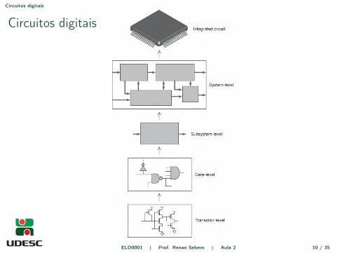
There are several ways of representing digital circuits, which depend on the intended level of abstrac-tion. Such levels are illustrated in Figure 1.6, where transistor-level is the lowest and system-level is the highest.
When using a transistor-level description, elementary components (transistors, diodes, resistors, capacitors, etc.) are explicitly shown in the schematics. In many cases, transistor-level circuits can be broken into several parts, each forming a gate (OR, AND, etc.). If gates are used
FIGURE 1.5. ASCII code.
ELD0001 ‡ Prof. Renan Sebem ‡ Aula 2 9 / 35
Circuitos digitais
Circuitos digitais
as the lowest level of abstraction, it is said to be a gate-level description for the design. After this point, nonstandard blocks (subsystems) are normally employed, which are collections of gate-level blocks that the designer creates to ease the visualization of the whole system. This is called subsystem-level description. Finally, by interconnecting the subsystem blocks, the complete system can be represented (system-level representation). At the top of Figure 1.6, an integrated circuit (IC) is shown, which is one of the alternatives that might be considered when physically implementing the design.
The most fundamental logic gates are depicted in Figure 1.7. Each has a name, a symbol, and a truth table (a truth table is simply a numeric translation of the gate’s binary function). The corresponding binary functions are listed below (the functions for three of them have already been given).
FIGURE 1.6. Representation of digital circuits according to the level of abstraction. The lowest level is the transistor-level, followed by gate-level representation, all the way up to a complete device.
1.4 Digital Circuits 7
ELD0001 ‡ Prof. Renan Sebem ‡ Aula 2 10 / 35
Circuitos digitais
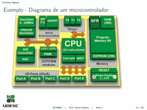
Exemplo - Diagrama de um microcontrolador
ELD0001 ‡ Prof. Renan Sebem ‡ Aula 2 11 / 35
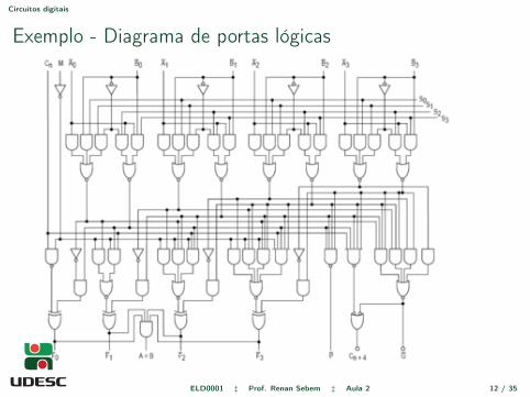
Circuitos digitais
Exemplo - Diagrama de portas lógicas
ELD0001 ‡ Prof. Renan Sebem ‡ Aula 2 12 / 35
Circuitos digitais
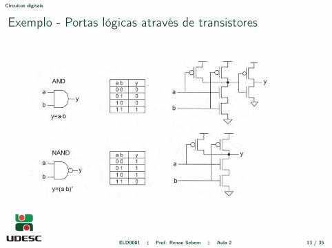
Exemplo - Portas lógicas através de transistores
78 CHAPTER 4 Introduction to Digital Circuits
The NAND circuit on the right of Figure 4.10(b) operates as follows. Suppose that a = '1' (= VDD) and b = '0' (= 0 V). In this case, the bottom nMOS transistor is OFF (due to b = '0') and the top one is ON (due to a = '1'). Reciprocally, the left pMOS is OFF (due to a = '1') and the right pMOS is ON (due to b = '0'). Because the nMOS transistors are connected in series (two switches in series), it suffi ces to have one of them OFF (open) for the branch to be disconnected from GND. On the other hand, the pMOS transistors are associated in parallel (switches in parallel), so it suffi ces to have one of them ON (closed) for that section to be connected to VDD. In summary, y is connected to VDD (and disconnected from GND), hence resulting y = '1' (= VDD) at the output. Only when both nMOS transistors are ON (and consequently both pMOS are OFF) will the output be connected to GND. This situation requires a = b = '1', so the circuit indeed computes the NAND function, y = (a ! b)".
EXAMPLE 4.2 TIMING DIAGRAM OF A COMBINATIONAL CIRCUIT
Consider the circuit shown in Figure 4.11(a).
a. Write the expression for y.
b. Suppose that the circuit is submitted to the stimuli a, b, and c depicted in the fi rst three wave-forms of Figure 4.11(b), where every time slot is 2 ns wide. Consider that the propagation delays through the AND and NAND gates are tp_AND = 4 ns and tp_NAND = 3 ns with the same value for the up and down transitions. Draw the corresponding waveforms for x and y, adopting the sim-plifi ed timing diagram style of Figure 4.8(b).
SOLUTION
a. y = (x ! c)" = (a ! b ! c)".
b. The resulting waveforms are included in Figure 4.11(b). Gray shades were used again to highlight the propagation delays (4 ns and 3 ns). Note that the delay sometimes gets accumu-lated (7 ns).
■
FIGURE 4.10. (a) AND gate and (b) NAND gate (symbol, truth table, and CMOS circuit).
ELD0001 ‡ Prof. Renan Sebem ‡ Aula 2 13 / 35
Circuitos digitais
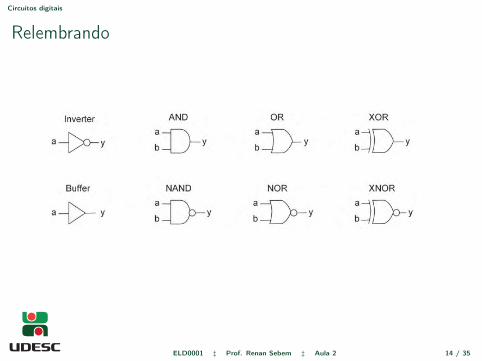
Relembrando
8 CHAPTER 1 Introduction
Inverter: Performs logical inversion.
y = a! or y = NOT aBuffer: Provides just the necessary currents and/or voltages at the output.y = aAND: Performs logical multiplication.y = a · b or y = a AND bNAND: Produces inverted logical multiplication.y = (a · b)! or y = NOT (a AND b)OR: Performs logical addition.y = a + b or y = a OR bNOR: Produces inverted logical addition.y = (a + b)! or y = NOT (a OR b)XOR: The output is '1' when the number of inputs that are '1' is odd.y = a ! b, y = a XOR b, or y = a · b! + a! · bXNOR: The output is '1' when the number of inputs that are '1' is even.y = (a ! b)!, y = a XNOR b, y = NOT (a XOR b), or y = a! · b! + a · b
The interpretation of the truth tables is straightforward. Take the AND function, for example; the output is '1' only when all inputs are '1', which is exactly what the corresponding binary function says.
The circuits described above, collectively called digital gates, have a very important point in common: None of them exhibits memory. In other words, the output depends solely on the current values of the inputs. Another group of elementary circuits, collectively called digital registers, is characterized by the oppo-site fact, that is, all have memory. Therefore, the output of such circuits depends on previous circuit states.
FIGURE 1.7. Fundamental logic gates (name, symbol, and truth table).
ELD0001 ‡ Prof. Renan Sebem ‡ Aula 2 14 / 35
Circuitos digitais
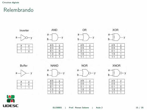
Relembrando
8 CHAPTER 1 Introduction
Inverter: Performs logical inversion.
y = a! or y = NOT aBuffer: Provides just the necessary currents and/or voltages at the output.y = aAND: Performs logical multiplication.y = a · b or y = a AND bNAND: Produces inverted logical multiplication.y = (a · b)! or y = NOT (a AND b)OR: Performs logical addition.y = a + b or y = a OR bNOR: Produces inverted logical addition.y = (a + b)! or y = NOT (a OR b)XOR: The output is '1' when the number of inputs that are '1' is odd.y = a ! b, y = a XOR b, or y = a · b! + a! · bXNOR: The output is '1' when the number of inputs that are '1' is even.y = (a ! b)!, y = a XNOR b, y = NOT (a XOR b), or y = a! · b! + a · b
The interpretation of the truth tables is straightforward. Take the AND function, for example; the output is '1' only when all inputs are '1', which is exactly what the corresponding binary function says.
The circuits described above, collectively called digital gates, have a very important point in common: None of them exhibits memory. In other words, the output depends solely on the current values of the inputs. Another group of elementary circuits, collectively called digital registers, is characterized by the oppo-site fact, that is, all have memory. Therefore, the output of such circuits depends on previous circuit states.
FIGURE 1.7. Fundamental logic gates (name, symbol, and truth table).
ELD0001 ‡ Prof. Renan Sebem ‡ Aula 2 15 / 35
Circuitos digitais
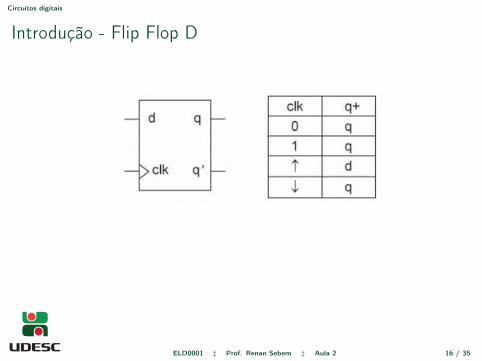
Introdução - Flip Flop D
Of all types of digital registers, the most commonly used is the D-type fl ip-fl op (DFF), whose symbol and truth table are depicted in Figure 1.8. The circuit has two inputs, called d (data) and clk (clock), and two outputs, called q and q! (where q! is the complement of q). Its operation can be summarized as fol-lows. Every time the clock changes from '0' to '1' (positive clock edge), the value of d is copied to q; during the rest of the time, q simply holds its value. In other words, the circuit is “transparent” at the moment when a positive edge occurs in the clock (represented by q+ = d in the truth table, where q+ indicates the circuit’s next state), and it is “opaque” at all other times (that is, q+ = q).
Two important conclusions can be derived from Figure 1.8. First, the circuit does indeed exhibit memory because it holds its state until another clock edge (of proper polarity) occurs. Second, registers are clocked, that is, need a signal, to control the sequence of events.
As will be described in detail in succeeding chapters, registers allow the construction of innumerous types of digital circuits. As an illustration, Figure 1.9 shows the use of a single DFF to construct a divide-by-2 frequency divider. All that is needed is to connect an inverted version of q back to the circuit’s input.
The circuit of Figure 1.9 operates as follows. The clock signal (a square wave that controls the whole sequence of events), shown in the upper plot of the timing diagram, is applied to the circuit. Because this is a positive-edge DFF, arrows are included in the clock waveform to highlight the only points where the DFF is transparent. The circuit’s initial state was assumed to be q = '0', so d = '1', which is copied to q at the next positive clock edge, producing q = '1' (after a little time delay, needed for the signal to traverse the fl ip-fl op). The new value of q now produces d = '0' (which also takes a little time to propagate through the inverter). Then, at the next positive clock transition, d is again copied to q, this time producing q = '0' and so on. Comparing the waveforms for clk and q, we observe that indeed the frequency of the latter is one-half that of the former.
In summary, the importance of registers is that they allow the construction of sequential logic circuits (defi ned below).
1.4 Digital Circuits 9
FIGURE 1.9. Application of a register (DFF) in the construction of a frequency divider.
FIGURE 1.8. Symbol and truth table for a positive-edge triggered D-type fl ip-fl op.
ELD0001 ‡ Prof. Renan Sebem ‡ Aula 2 16 / 35

Circuitos digitais
Introdução - Flip Flop D - Diagrama temporal
Of all types of digital registers, the most commonly used is the D-type fl ip-fl op (DFF), whose symbol and truth table are depicted in Figure 1.8. The circuit has two inputs, called d (data) and clk (clock), and two outputs, called q and q! (where q! is the complement of q). Its operation can be summarized as fol-lows. Every time the clock changes from '0' to '1' (positive clock edge), the value of d is copied to q; during the rest of the time, q simply holds its value. In other words, the circuit is “transparent” at the moment when a positive edge occurs in the clock (represented by q+ = d in the truth table, where q+ indicates the circuit’s next state), and it is “opaque” at all other times (that is, q+ = q).
Two important conclusions can be derived from Figure 1.8. First, the circuit does indeed exhibit memory because it holds its state until another clock edge (of proper polarity) occurs. Second, registers are clocked, that is, need a signal, to control the sequence of events.
As will be described in detail in succeeding chapters, registers allow the construction of innumerous types of digital circuits. As an illustration, Figure 1.9 shows the use of a single DFF to construct a divide-by-2 frequency divider. All that is needed is to connect an inverted version of q back to the circuit’s input.
The circuit of Figure 1.9 operates as follows. The clock signal (a square wave that controls the whole sequence of events), shown in the upper plot of the timing diagram, is applied to the circuit. Because this is a positive-edge DFF, arrows are included in the clock waveform to highlight the only points where the DFF is transparent. The circuit’s initial state was assumed to be q = '0', so d = '1', which is copied to q at the next positive clock edge, producing q = '1' (after a little time delay, needed for the signal to traverse the fl ip-fl op). The new value of q now produces d = '0' (which also takes a little time to propagate through the inverter). Then, at the next positive clock transition, d is again copied to q, this time producing q = '0' and so on. Comparing the waveforms for clk and q, we observe that indeed the frequency of the latter is one-half that of the former.
In summary, the importance of registers is that they allow the construction of sequential logic circuits (defi ned below).
1.4 Digital Circuits 9
FIGURE 1.9. Application of a register (DFF) in the construction of a frequency divider.
FIGURE 1.8. Symbol and truth table for a positive-edge triggered D-type fl ip-fl op.
ELD0001 ‡ Prof. Renan Sebem ‡ Aula 2 17 / 35
Circuitos digitais
Lógica combinacional vs. Lógica sequencial
I Os dois tipos de lógica utilizam portas lógicas;I A lógica combinacional depende estritamente das entradas atuais;I A lógica sequencial depende, além das entradas atuais, das entradas
passadas;I Flip flops são utilizados para formar um circuito de lógica sequancial;I Nem todos os circuitos com flip flops são sequenciais;
ELD0001 ‡ Prof. Renan Sebem ‡ Aula 2 18 / 35
Circuitos digitais
Circuitos integradosSão classificados principalmente através das seguintes características:
I Escala de integração;I Tensão de alimentação;I Tipo de encapsulamento;I Tipo de transistor;I Família lógica;
ELD0001 ‡ Prof. Renan Sebem ‡ Aula 2 19 / 35
Circuitos digitais
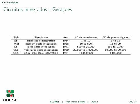
Circuitos integrados - Gerações
Sigla Significado Ano No de transistores No de portas lógicasSSI small-scale integration 1964 1 to 10 1 to 12MSI medium-scale integration 1968 10 to 500 13 to 99LSI large-scale integration 1971 500 to 20,000 100 to 9,999VLSI very large-scale integration 1980 20,000 to 1,000,000 10,000 to 99,999ULSI ultra-large-scale integration 1984 +1,000,000 +100,000
ELD0001 ‡ Prof. Renan Sebem ‡ Aula 2 20 / 35
Circuitos digitais
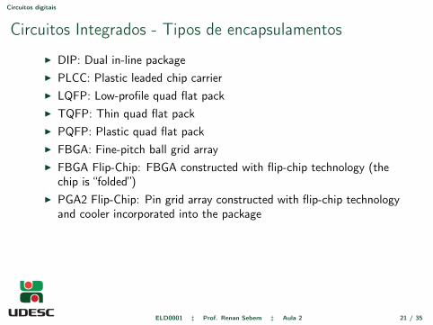
Circuitos Integrados - Tipos de encapsulamentos
I DIP: Dual in-line packageI PLCC: Plastic leaded chip carrierI LQFP: Low-profile quad flat packI TQFP: Thin quad flat packI PQFP: Plastic quad flat packI FBGA: Fine-pitch ball grid arrayI FBGA Flip-Chip: FBGA constructed with flip-chip technology (the
chip is “folded”)I PGA2 Flip-Chip: Pin grid array constructed with flip-chip technology
and cooler incorporated into the package
ELD0001 ‡ Prof. Renan Sebem ‡ Aula 2 21 / 35
Circuitos digitais
Circuitos Integrados - Tipos de encapsulamentos12 CHAPTER 1 Introduction
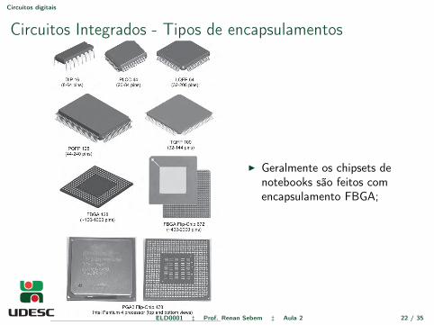
FIGURE 1.10. Examples of IC packages, each accompanied by name, number of pins, and typical range of pins (between parentheses) for that package type. When the number of pins is not too large (< 300), they can be located on the sides of the IC, while in larger packages they are located under the chip. In the latter, two main approaches exist, called BGA (ball grid array, shown in the third row) and PGA (pin grid array, shown in the last row). Pentium 4 microprocessor reprinted with permission of Intel.
I Geralmente os chipsets denotebooks são feitos comencapsulamento FBGA;
ELD0001 ‡ Prof. Renan Sebem ‡ Aula 2 22 / 35
Circuitos digitais
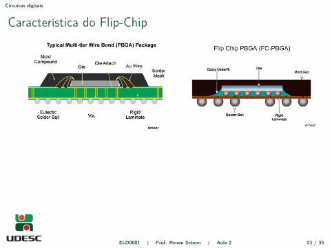
Característica do Flip-Chip
ELD0001 ‡ Prof. Renan Sebem ‡ Aula 2 23 / 35
Circuitos digitais
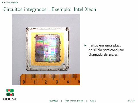
Circuitos integrados - Exemplo: Intel Xeon
I Feitos em uma placade silício semicondutorchamada de wafer.
ELD0001 ‡ Prof. Renan Sebem ‡ Aula 2 24 / 35
Circuitos digitais
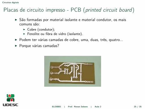
Placas de circuito impresso - PCB (printed circuit board)
I São formadas por material isolante e material condutor, os maiscomuns são:
I Cobre (condutor);I Fenolite ou fibra de vidro (isolante).
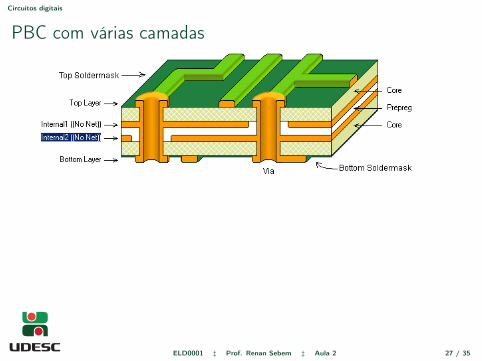
I Podem ter várias camadas de cobre, uma, duas, três, quatro...I Porque várias camadas?
ELD0001 ‡ Prof. Renan Sebem ‡ Aula 2 25 / 35
Circuitos digitais
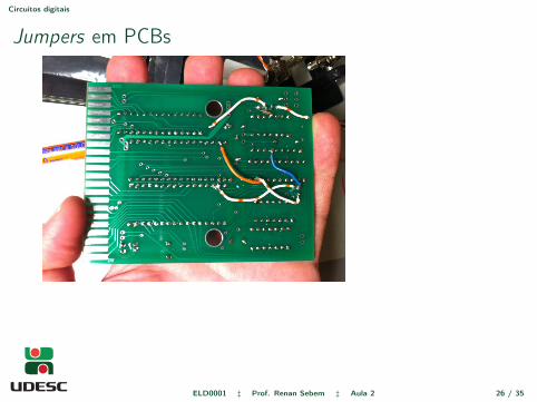
Jumpers em PCBs
ELD0001 ‡ Prof. Renan Sebem ‡ Aula 2 26 / 35
Circuitos digitais
PBC com várias camadas
ELD0001 ‡ Prof. Renan Sebem ‡ Aula 2 27 / 35
Circuitos digitais
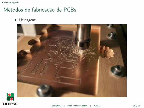
Métodos de fabricação de PCBs
I Usinagem:
ELD0001 ‡ Prof. Renan Sebem ‡ Aula 2 28 / 35
Circuitos digitais
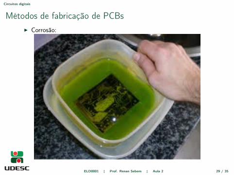
Métodos de fabricação de PCBsI Corrosão:
ELD0001 ‡ Prof. Renan Sebem ‡ Aula 2 29 / 35
Composição de portas lógicas através de transistores
Conceitos iniciais
I Resistor de pull-up e pull-down;I Funcionamento do transistor.
ELD0001 ‡ Prof. Renan Sebem ‡ Aula 2 30 / 35
Composição de portas lógicas através de transistores
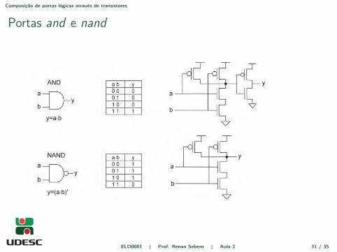
Portas and e nand
78 CHAPTER 4 Introduction to Digital Circuits
The NAND circuit on the right of Figure 4.10(b) operates as follows. Suppose that a = '1' (= VDD) and b = '0' (= 0 V). In this case, the bottom nMOS transistor is OFF (due to b = '0') and the top one is ON (due to a = '1'). Reciprocally, the left pMOS is OFF (due to a = '1') and the right pMOS is ON (due to b = '0'). Because the nMOS transistors are connected in series (two switches in series), it suffi ces to have one of them OFF (open) for the branch to be disconnected from GND. On the other hand, the pMOS transistors are associated in parallel (switches in parallel), so it suffi ces to have one of them ON (closed) for that section to be connected to VDD. In summary, y is connected to VDD (and disconnected from GND), hence resulting y = '1' (= VDD) at the output. Only when both nMOS transistors are ON (and consequently both pMOS are OFF) will the output be connected to GND. This situation requires a = b = '1', so the circuit indeed computes the NAND function, y = (a ! b)".
EXAMPLE 4.2 TIMING DIAGRAM OF A COMBINATIONAL CIRCUIT
Consider the circuit shown in Figure 4.11(a).
a. Write the expression for y.
b. Suppose that the circuit is submitted to the stimuli a, b, and c depicted in the fi rst three wave-forms of Figure 4.11(b), where every time slot is 2 ns wide. Consider that the propagation delays through the AND and NAND gates are tp_AND = 4 ns and tp_NAND = 3 ns with the same value for the up and down transitions. Draw the corresponding waveforms for x and y, adopting the sim-plifi ed timing diagram style of Figure 4.8(b).
SOLUTION
a. y = (x ! c)" = (a ! b ! c)".
b. The resulting waveforms are included in Figure 4.11(b). Gray shades were used again to highlight the propagation delays (4 ns and 3 ns). Note that the delay sometimes gets accumu-lated (7 ns).
■
FIGURE 4.10. (a) AND gate and (b) NAND gate (symbol, truth table, and CMOS circuit).
ELD0001 ‡ Prof. Renan Sebem ‡ Aula 2 31 / 35
Composição de portas lógicas através de transistores
Inversor CMOS
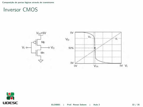
DC responseDC response is the response of a circuit to a large amplitude slowly varying stimulus. DC stands for direct current, meaning a constant electric current of voltage. The name “DC response” therefore indicates that each output value is measured for a fi xed input value. In other words, the input signal is varied a little, then enough time is given for the output signal to completely settle, and only then are the measurements taken. During the tests, a large range is covered by the input signal. This type of analysis will be studied in Sections 8.4 (for BJT-based circuits) and 9.4 (for MOS-based circuits).
An example of DC response is presented in Figure 1.15, which shows the voltage at the output of a CMOS inverter (Section 9.5) when its input is subject to a slowly varying voltage ranging from GND (0 V) to VDD (5 V in this example). When the input is low, the output is high, and vice versa. However, there is a point somewhere between the two extremes where the circuit changes its condition. This volt-age is called transition voltage (VTR) and is measured at the midpoint between the two logic voltages (GND and VDD). In this example, VTR ! 2.2 V.
Transient responseTransient response represents the response of a circuit to a large-amplitude fast-varying stimulus. This type of analysis, also called time response, will be seen several times in subsequent chapters, particularly in Sections 8.5 (for BJT-based circuits) and 9.6 (for MOS-based circuits).
An example is shown in Figure 1.16. It is indeed a continuation of Figure 1.13, now with a more real-istic representation. The transient response is specifi ed by means of a series of parameters whose defi ni-tions are presented below.
tr (rise time): Time needed for the output to rise from 10% to 90% of its static valuestf (fall time): Time needed for the output to fall from 90% to 10% of its static valuestpLH (low-to-high propagation delay): Time delay between the input crossing 50% and the output cross-ing 50% when the output risestpHL (high-to-low propagation delay): Time delay between the input crossing 50% and the output cross-ing 50% when the output fallston (turn-on delay): Time delay between the input crossing 10% and the output crossing 90% when the switch closes (rising edge when displaying current)toff (turn-off delay): Time delay between the input crossing 90% and the output crossing 10% when the switch opens (falling edge when displaying current)
Note in Figure 1.16 that the fi rst two parameters, tr and tf, represent local measurements (they concern only one signal, the output), while the others are transfer parameters (they relate one side of the circuit to the other, that is, input-output). For that reason, the latter are more representative, so they are more
1.11 DC, AC, and Transient Responses 17
FIGURE 1.15. DC response of a CMOS inverter.
ELD0001 ‡ Prof. Renan Sebem ‡ Aula 2 32 / 35
Composição de portas lógicas através de transistores
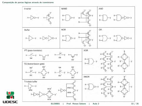
OR: y = a + b (this is a NOR gate followed by an inverter)
XOR: y = a ! b = a! · b + a · b! (two implementations are presented in Figure 11.2, one with CMOS logic, the other with TG-logic)
XNOR: y = (a ! b)! = a! · b! + a · b (again, two implementations are included in Figure 11.2, one with CMOS logic, the other with TG-logic)
11.4 Compound GatesHaving reviewed the fundamental logic gates, we now examine the constructions of larger gates. Because they combine functions performed by different basic gates (notably AND, OR, and inversion), they are referred to as compound gates.
It was seen in Chapter 5 that any logic function can be expressed as a sum-of-products (SOP), like y = a · b + c · d, or as a product-of-sums (POS), like y = (a + b) · (c + d). In this section we show how to draw a circuit for each of these expressions.
■
■
■
11.4 Compound Gates 259
FIGURE 11.2. Fundamental logic gates (symbols followed by examples of MOS-based implementations).ELD0001 ‡ Prof. Renan Sebem ‡ Aula 2 33 / 35
Bibliografia
[1] Volnei A. Pedroni. Eletrônica digital moderna e VHDL: Princípiosdigitais, Eletrônica Digital, Projeto DIgital, Microeletrônica e VHDL.Elsevier, 2010.
ELD0001 ‡ Prof. Renan Sebem ‡ Aula 2 34 / 35
Aula 2 - Indrotução à eletrônica digital
Prof. Renan Sebem
Disciplina de Eletrônica DigitalGraduação em Engenharia Elétrica
Universidade do Estado de Santa CatarinaJoinville-SC – Brasil
25 de fevereiro de 2016
Obrigado.
ELD0001 ‡ Prof. Renan Sebem ‡ Aula 2 35 / 35
![Liver Transplantation outcome prediction - A …...Despite significant improvements over the years in the results of liver transplantation (LT) [1], primary graft dysfunction (PGD)](https://img.document.onl/doc/110x75/5f9bbaccdc4bd5770f3bedfd/liver-transplantation-outcome-prediction-a-despite-significant-improvements.jpg)