Embed Size (px)
Citation preview

Aula 6 - Geração de funções booleanas através dedecodificadores e multiplexadores
Prof. Renan Sebem
Disciplina de Eletrônica Digital
Graduação em Engenharia Elétrica
Universidade do Estado de Santa Catarina
Joinville-SC – Brasil
8 de março de 2016
ELD0001 ‡ Prof. Renan Sebem ‡ Aula 6 1 / 12

Conteúdo da Aula
Relembrando Minitermos e maxitermos
Gerando funções com decodificadores
Gerando funções com multiplexadores
Transformando um demultiplexador em um decodificador
Itens adicionais
Bibliografia
ELD0001 ‡ Prof. Renan Sebem ‡ Aula 6 2 / 12
Relembrando Minitermos e maxitermos
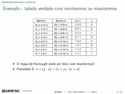
Exemplo - tabela verdade com minitermos ou maxitermos
Let us consider the function y = f (a, b, c) given below:
y = a! " b " c! + a " b " c! + a " b " c (5.9a)
Because all terms in Equation 5.9(a) are minterms, this expression is referred to as minterm expansion. Moreover, because it is also a sum of products, it is called SOP equation (SOP format).
The truth table for Equation 5.9(a) is presented in Figure 5.5 with the corresponding minterms also included (represented by mi, where i is the decimal value represented by abc in that row of the truth table). Note that y = '1' occurs only for the minterms that appear in Equation 5.9(a), so another representa-tion for that equation is the following:
y = m2 + m6 + m7 (5.9b)
Or, equivalently:
y = ! m (2, 6, 7) (5.9c)
Every term of an SOP is called an implicant because when that term is '1' the function is '1' too. There-fore, all minterms that cause y = '1' are implicants of y. However, not all minterms are prime implicants.
A prime implicant is an implicant from which no literal can be removed. To illustrate this concept, let us examine Equation 5.9(a) again. That function can be simplifi ed to the following (simplifi cation tech-niques will be discussed ahead):
y = a " b + b " c! (5.9d)
Equation 5.9(d) has two terms from which no literal can be further removed, so a " b and b " c! are prime implicants of y. Note that in this particular example neither prime implicant is a minterm.
EXAMPLE 5.8 MINTERMS AND PRIME IMPLICANTS
Consider the irreducible function of four variables y = a! " c! + a! " b! " d! + a " b " c " d. Which terms are minterms and which are prime implicants?
SOLUTION
Because the equation is irreducible, all three terms are prime implicants. However, only one of them has four literals, that is, only a " b " c " d is a minterm (= m15).
■
FIGURE 5.5. Truth table for y = a! " b " c! + a " b " c! + a " b " c (minterm expansion).
5.3 Minterms and SOP Equations 109
I O mapa de Karnaugh pode ser feito com maxitermos?I Postulado 6: x + (y · z) = (x + y) · (x + z)
ELD0001 ‡ Prof. Renan Sebem ‡ Aula 6 3 / 12

Relembrando Minitermos e maxitermos
Exemplo - Multiplexador de duas portas
I Tabela verdade do multiplexador de duas portas:
Entradas SaídaS b a Y0 0 0 00 0 1 10 1 0 00 1 1 11 0 0 01 0 1 01 1 0 11 1 1 1
ELD0001 ‡ Prof. Renan Sebem ‡ Aula 6 4 / 12

Gerando funções com decodificadores
Exemplo - Decodificador de 2/4 bits gerando função XOREntradas Saídas
enable x
1
x
0
y
3
y
2
y
1
y
0
0 X X 0 0 0 0
1
0 0 0 0 0 10 1 0 0 1 01 0 0 1 0 01 1 1 0 0 0
The circuit shown in Figure 11.8(b) is a direct implementation of the SOP expressions listed above using AND gates. In Figure 11.8(c), a CMOS architecture is depicted, which was obtained using the POS equations and the procedure described in Section 11.4 (notice that some of the transistors are shared between adjacent branches), thus resulting in a NOR gate in each column. In Figure 11.8(d), pseudo-nMOS logic was employed instead of CMOS, again based on the POS expressions (so each column is still a NOR gate). Finally, in Figure 11.8(e), footed dynamic logic was employed, and the implementation was based on the SOP expressions instead of POS, thus resulting in NAND gates in the columns (in this case, the dissimilar bit is low instead of high).
11.5 Encoders and Decoders 263
FIGURE 11.7. (a) Address decoder symbols; (b) Truth table for N = 3, with the dissimilar bit equal to '1' (“one-hot” code).
FIGURE 11.8. Address decoder implementations for N = 2: (a) Truth table; (b) SOP-based implementation with AND gates; (c) POS-based CMOS implementation (columns are NOR gates); (d) POS-based pseudo-nMOS implementation (again columns are NOR gates); (e) SOP-based footed dynamic implementation (columns are NAND gates). The dissimilar bit is high in all circuits except in (e).
ELD0001 ‡ Prof. Renan Sebem ‡ Aula 6 5 / 12

Gerando funções com decodificadores
Exemplo - Função booleana arbitrária de 4 variáveisEntradas Saída
x3 x2 x1 x0 Y0 0 0 0 00 0 0 1 10 0 1 0 00 0 1 1 10 1 0 0 10 1 0 1 10 1 1 0 00 1 1 1 01 0 0 0 11 0 0 1 01 0 1 0 01 0 1 1 01 1 0 0 01 1 0 1 11 1 1 0 11 1 1 1 0
ELD0001 ‡ Prof. Renan Sebem ‡ Aula 6 6 / 12
Gerando funções com multiplexadores
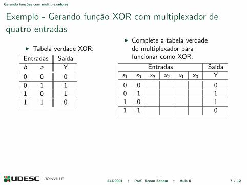
Exemplo - Gerando função XOR com multiplexador dequatro entradas
I Tabela verdade XOR:Entradas Saídab a Y0 0 00 1 11 0 11 1 0
I Complete a tabela verdadedo multiplexador parafuncionar como XOR:
Entradas Saídas
1
s
0
x
3
x
2
x
1
x
0
Y0 0 00 1 11 0 11 1 0
ELD0001 ‡ Prof. Renan Sebem ‡ Aula 6 7 / 12

Gerando funções com multiplexadores
Exemplo - Função booleana arbitrária de 4 variáveisEntradas Saída
s3 s2 s1 s0 x7 x6 x5 x4 x3 x2 x1 x0 Y0 0 0 0 00 0 0 1 10 0 1 0 00 0 1 1 10 1 0 0 10 1 0 1 10 1 1 0 00 1 1 1 01 0 0 0 11 0 0 1 01 0 1 0 01 0 1 1 01 1 0 0 01 1 0 1 11 1 1 0 11 1 1 1 0
ELD0001 ‡ Prof. Renan Sebem ‡ Aula 6 8 / 12
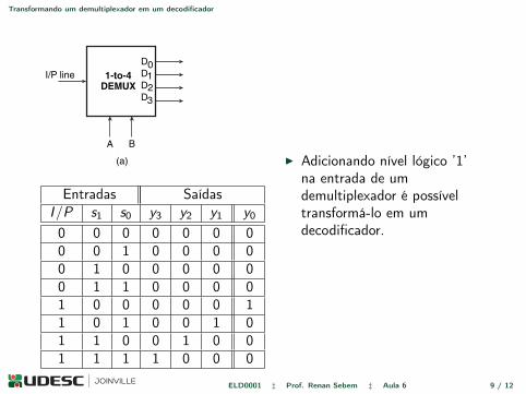
Transformando um demultiplexador em um decodificador
Multiplexers and Demultiplexers 285
X
D1
D3
D2
Y
Figure 8.17 Example 8.5.
8.3 Demultiplexers and DecodersA demultiplexer is a combinational logic circuit with an input line, 2n output lines and n select lines. Itroutes the information present on the input line to any of the output lines. The output line that gets theinformation present on the input line is decided by the bit status of the selection lines. A decoder is aspecial case of a demultiplexer without the input line. Figure 8.18(a) shows the circuit representationof a 1-to-4 demultiplexer. Figure 8.18(b) shows the truth table of the demultiplexer when the inputline is held HIGH.
A decoder, as mentioned earlier, is a combinational circuit that decodes the information on n inputlines to a maximum of 2n unique output lines. Figure 8.19 shows the circuit representation of 2-to-4,3-to-8 and 4-to-16 line decoders. If there are some unused or ‘don’t care’ combinations in the n-bitcode, then there will be fewer than 2n output lines. As an illustration, if there are three input lines, it
(b)
I/P
1111
A0011
B0101
D01000
D10100
D20010
D30001
1-to-4DEMUX
I/P line
A B
D0D1D2D3
Select O/P
(a)
Figure 8.18 1-to-4 demultiplexer.
Entradas SaídasI/P s
1
s
0
y
3
y
2
y
1
y
0
0 0 0 0 0 0 00 0 1 0 0 0 00 1 0 0 0 0 00 1 1 0 0 0 01 0 0 0 0 0 11 0 1 0 0 1 01 1 0 0 1 0 01 1 1 1 0 0 0
I Adicionando nível lógico ’1’na entrada de umdemultiplexador é possíveltransformá-lo em umdecodificador.
ELD0001 ‡ Prof. Renan Sebem ‡ Aula 6 9 / 12
Itens adicionais
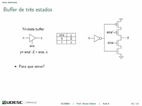
Buffer de três estados
That in (c) shows a buffer employed to restore a “weak” signal (in long-distance transmissions or noisy environments). Buffers with a large current capacity (normally many milliamperes) are also referred to as drivers (employed as line drivers and bus drivers, for example).
4.8 Tri-State BufferThe circuit in Figure 4.18 is called a tri-state buffer (also three-state buffer or 3-state buffer) because it has a third state, called 'Z', which represents high impedance. In other words, when the circuit is enabled (ena = '1'), it operates as a regular buffer, whereas when disabled (ena = '0'), the output node is discon-nected from the internal circuitry. Its logical function is therefore that shown below.
Tri-state buffer function:
y = ena! " Z + ena " x (4.17)
A typical CMOS circuit for this buffer is also included in Figure 4.18, which consists of a CMOS inverter followed by a C2MOS inverter (C2MOS logic will be studied in Chapter 10). Note that when ena = '1', both inner transistors are ON (because '1' is applied to the gate of the nMOS and '0' to the gate of the pMOS), so the outer transistors are connected to the output node (y), rendering a regular CMOS inverter. How-ever, when ena = '0', both inner transistors are turned OFF (because now the nMOS receives '0' and the pMOS receives '1'), causing node y to be disconnected from all transistors (node y is left “fl oating”).
The construction of multi-bit buffers is straightforward. As illustrated in Figure 4.19, an N-bit buffer consists simply of N single-bit units sharing the same buffer-enable (ena) signal. Two equivalent
FIGURE 4.18. Tri-state buffer (symbol, truth table, and CMOS-C2MOS implementation).
4.8 Tri-State Buffer 85
FIGURE 4.19. Construction of a multi-bit tri-state buffer (two equivalent representations are shown on the right).
I Para que serve?
ELD0001 ‡ Prof. Renan Sebem ‡ Aula 6 10 / 12

Bibliografia
[1] Mairton de Oliveira Melo. Eletrônica Digital – Teoria e Laboratório.Editora Udesc, 2002.
ELD0001 ‡ Prof. Renan Sebem ‡ Aula 6 11 / 12
Aula 6 - Geração de funções booleanas através dedecodificadores e multiplexadores
Prof. Renan Sebem
Disciplina de Eletrônica Digital
Graduação em Engenharia Elétrica
Universidade do Estado de Santa Catarina
Joinville-SC – Brasil
8 de março de 2016
Obrigado.
ELD0001 ‡ Prof. Renan Sebem ‡ Aula 6 12 / 12