Embed Size (px)
Citation preview

BL1700C-Programmable Controller
Users ManualRevision E
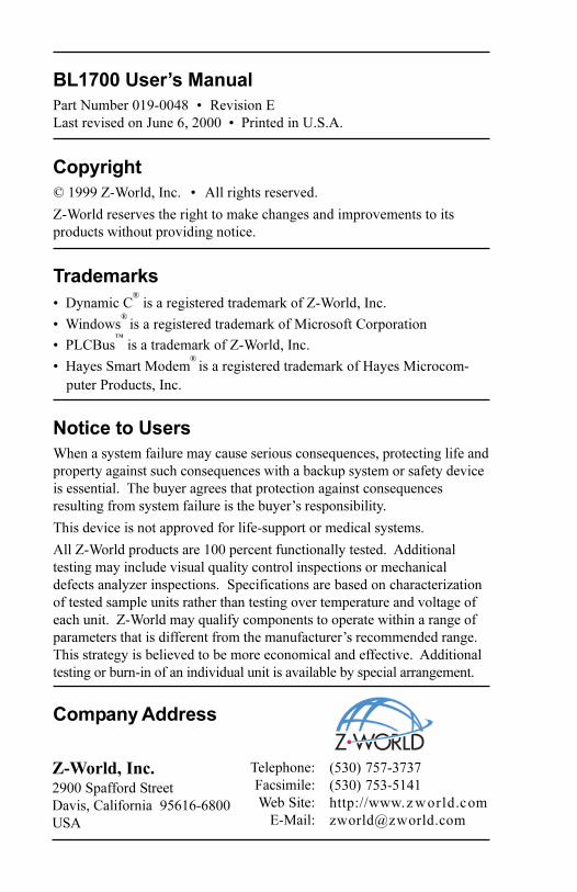
BL1700 Users ManualPart Number 019-0048
Revision E
Last revised on June 6, 2000 Printed in U.S.A.
Copyright© 1999 Z-World, Inc.
All rights reserved.
Z-World reserves the right to make changes and improvements to itsproducts without providing notice.
Trademarks Dynamic C
® is a registered trademark of Z-World, Inc.
Windows®
is a registered trademark of Microsoft Corporation
PLCBus
is a trademark of Z-World, Inc.
Hayes Smart Modem®
is a registered trademark of Hayes Microcom-puter Products, Inc.
Notice to UsersWhen a system failure may cause serious consequences, protecting life andproperty against such consequences with a backup system or safety deviceis essential. The buyer agrees that protection against consequencesresulting from system failure is the buyers responsibility.
This device is not approved for life-support or medical systems.
All Z-World products are 100 percent functionally tested. Additionaltesting may include visual quality control inspections or mechanicaldefects analyzer inspections. Specifications are based on characterizationof tested sample units rather than testing over temperature and voltage ofeach unit. Z-World may qualify components to operate within a range ofparameters that is different from the manufacturers recommended range.This strategy is believed to be more economical and effective. Additionaltesting or burn-in of an individual unit is available by special arrangement.
Company Address
Z-World, Inc.2900 Spafford StreetDavis, California 95616-6800USA
Telephone:Facsimile:Web Site:
E-Mail:
(530) 757-3737(530) 753-5141http://www.z w [email protected]
Contents s iiiBL1700
TABLE OF CONTENTS
About This Manual vii
Chapter 1: Overview 11Overview .............................................................................................. 12Features ................................................................................................ 13Flexibility and Customization .............................................................. 14
Standard Models ............................................................................. 14Customization Options .................................................................... 14
Development and Evaluation Tools ..................................................... 15Development Kit ............................................................................. 15Software .......................................................................................... 15
CE Compliance .................................................................................... 16
Chapter 2: Getting Started 17Development Kit Packing List ............................................................. 18Connecting the BL1700 to a Host PC .................................................. 18Establishing Communication with the BL1700 ................................... 21Running a Sample Program ................................................................. 22
Chapter 3: BL1700 Hardware 23Operating Modes ................................................................................. 24
Changing the Operating Mode ........................................................ 25Run Mode ........................................................................................ 26
BL1700 Subsystems Overview ............................................................ 27Microprocessor Core Module ......................................................... 27
Core Module External Connections .............................................. 28Digital Inputs and Outputs ................................................................... 29
External Connections ...................................................................... 30Digital Inputs ................................................................................... 31
Operating Modes and Configuration ............................................ 31Digital Outputs ................................................................................ 34
Operating Modes and Configuration ............................................ 34High-Voltage Drivers .................................................................... 34Pulse-Width Modulation (PWM) Configuration .......................... 37
iv s Contents BL1700
Analog Inputs ....................................................................................... 38Operating Modes and Configuration ............................................... 38
Drift .............................................................................................. 45Low-Pass Filter ............................................................................. 45Excitation Resistors ...................................................................... 46
Using the Unconditioned Converter Channels ................................ 46Internal Test Voltages ...................................................................... 46Power-Down Mode ......................................................................... 47External Connections ...................................................................... 47
Serial Channels .................................................................................... 48Operating Modes and Configuration ............................................... 49Configuring a Multidrop Network .................................................. 51
RS-485 Termination ...................................................................... 51External Connections ...................................................................... 51
PLCBus ................................................................................................ 55Operating Modes and Configuration ............................................... 55External Connections ...................................................................... 55
Chapter 4: Software Development 57Supplied Software ................................................................................ 58Digital Inputs ....................................................................................... 59
How to Read the Input .................................................................... 59Sample Program .............................................................................. 60
Digital Outputs ..................................................................................... 61Sample Program .............................................................................. 62
Pulse-Width Modulated (PWM) Outputs ............................................ 63How to Use the PWM Feature ........................................................ 63PWM Software ................................................................................ 65Sample Program .............................................................................. 66
Analog Inputs ....................................................................................... 67Using the Analog Inputs .................................................................. 67Sample Program .............................................................................. 69
Serial Channels .................................................................................... 70RS-232 Communication .................................................................. 70RS-485 Communication .................................................................. 70Software .......................................................................................... 71Sample Program .............................................................................. 71
LED...................................................................................................... 72Additional Software ............................................................................. 72
Contents s vBL1700
Appendix A: Troubleshooting 73Out of the Box...................................................................................... 74LCD Connected to BL1700 Does Not Work ....................................... 74Dynamic C Will Not Start .................................................................... 75BL1700 Resets Repeatedly .................................................................. 76Troubleshooting Software .................................................................... 76
Appendix B: Specifications 77Electronic and Mechanical Specifications ........................................... 78
BL1700 Mechanical Dimensions .................................................... 79Header and Jumper Information .......................................................... 80Protected Digital Inputs ....................................................................... 85
Frequency Response for the Protected Inputs ................................. 86High-Voltage Drivers ........................................................................... 87
Sinking Driver ................................................................................. 87Sourcing Driver ............................................................................... 88
Appendix C: Field Wiring Terminals (FWT)and DIN Rails 89
Field Wiring Terminals ........................................................................ 90FWT38 ............................................................................................ 91FWT50 ............................................................................................ 92FWT-Opto ....................................................................................... 94FWT-A/D ........................................................................................ 97
DIN Rails ............................................................................................. 98
Appendix D: Sinking and Sourcing Drivers 99BL1700 Series Sinking and Sourcing Outputs ................................... 100
Installing Sourcing Drivers ........................................................... 102TTL/CMOS Outputs .......................................................................... 103Using Output Drivers ......................................................................... 103
Appendix E: PLCBus 105PLCBus Overview ............................................................................. 106Allocation of Devices on the Bus ...................................................... 110
4-Bit Devices ................................................................................ 1108-Bit Devices ................................................................................ 111
Expansion Bus Software .................................................................... 111
vi s Contents BL1700
Appendix F: Serial Interface Board 2 117Introduction ........................................................................................ 118External Dimensions .......................................................................... 119
Appendix G: Advanced Topics 121Power Management ........................................................................... 122
Power Failure Detection Circuitry ................................................ 122Power Failure Sequence of Events ................................................ 122
Memory Map ..................................................................................... 124Input/Output Select Map ............................................................... 124Z180 Internal Input/Output Register Addresses 0x00-0x3F ......... 124BL1700 Peripheral Addresses ....................................................... 126Epson 72423 Timer Registers 0x41800x418F ............................ 127
Interrupts ............................................................................................ 128Interrupt Service Routines............................................................. 128Interrupt Vectors ............................................................................ 129Jump Vectors ................................................................................. 130
Flash EPROM .................................................................................... 131Simulated EEPROM ..................................................................... 131Other Flash EPROM Software ...................................................... 132
Pulse-Width Modulation (PWM) Software ....................................... 133PWM Addressing Detail ............................................................... 133PWM Software .............................................................................. 137Sample Program ............................................................................ 139
Appendix H: Battery 141Battery Life and Storage Conditions .................................................. 142Replacing Soldered Lithium Battery .................................................. 142Battery Cautions ................................................................................ 143
Index 145
BL1700 About This Manual s vii
ABOUT THIS MANUAL
This manual provides instructions for installing, testing, configuring, andinterconnecting the Z-World BL1700 controller. Instructions are alsoprovided for using Dynamic C functions.
AssumptionsAssumptions are made regarding the user's knowledge and experience inthe following areas:
Ability to design and engineer the target system that a BL1700 willcontrol.
Understanding of the basics of operating a software program andediting files under Windows on a PC.
Knowledge of the basics of C programming.
For a full treatment of C, refer to the following texts.
The C Programming Language by Kernighan and RitchieC: A Reference Manual by Harbison and Steel
Knowledge of basic Z80 assembly language and architecture.
For documentation from Zilog, refer to the following texts.
Z180 MPU User's ManualZ180 Serial Communication ControllersZ80 Microprocessor Family User's Manual
$
$

BL1700viii s About This Manual
AcronymsTable 1 lists and defines the acronyms that may be used in this manual.
IconsTable 2 displays and defines icons that may be used in this manual.
Table 1. Acronyms
Acronym Meaning
EPROM Erasable Programmable Read-Only Memory
EEPROM Electronically Erasable Programmable Read-Only Memory
LCD Liquid Crystal Display
LED Light-Emitting Diode
NMI Nonmaskable Interrupt
PIO Parallel Input/Output Circuit(Individually Programmable Input/Output)
PRT Programmable Reload Timer
RAM Random Access Memory
RTC Real-Time Clock
SIB Serial Interface Board
SRAM Static Random Access Memory
UART Universal Asynchronous Receiver Transmitter
Table 2. Icons
Icon Meaning Icon Meaning
$ Refer to or see ! Note
( Please contact 7LS Tip
Caution High Voltage
)'
Factory Default
BL1700 About This Manual s ix
ConventionsTable 3 lists and defines the typographic conventions that may be used inthis manual.
Pin Number 1A black square indicatespin 1 of all headers.
MeasurementsAll diagram and graphic measurements are in inches followed by millime-ters enclosed in parenthesis.
Table 3. Typographic Conventions
Example Description
while Courier font (bold) indicates a program, a fragment of aprogram, or a Dynamic C keyword or phrase.
// IN-01… Program comments are written in Courier font, plain face.
Italics Indicates that something should be typed instead of theitalicized words (e.g., in place of filename, type a file’sname).
Edit Sans serif font (bold) signifies a menu or menu selection.
. . . An ellipsis indicates that (1) irrelevant program text isomitted for brevity or that (2) preceding program text maybe repeated indefinitely.
[ ] Brackets in a C function’s definition or program segmentindicate that the enclosed directive is optional.
< > Angle brackets occasionally enclose classes of terms.
a | b | c A vertical bar indicates that a choice should be made fromamong the items listed.
J1Pin 1

BL1700x s About This Manual
Blank

BL1700 Overview s 11
CHAPTER 1: OVERVIEW
Chapter 1 provides an overview and a brief description of the BL1700features.

BL170012 s Overview
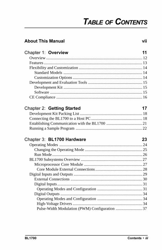
OverviewThe BL1700 is a feature-rich controller with modular digital and analogI/O that allows easy custom modification. The BL1700 is programmedusing Dynamic C, Z-Worlds version of the C programming languagedesigned for embedded control.
Figure 1-1 illustrates the BL1700 board layout.
Figure 1-1. BL1700 Board Layout
Battery
SCC
H1
J5
H4 C1
J4
U2
D1
U13
U14
J6
H5
U20
MV1 MV2 MV3 MV4 MV5 MV6
C7
H13 H14 H15
J8
L1
J7
C6
C12 C13 C14
J3
H3H2J2
RN1
H12
J1
SW1
D2
U9
U12
U19
U4
U8
U11
U18
U22
H10 H8U24
U23
U17
U7
H9
H6 H7
U15
U5
U1
U3
U6
U10
U16
U21
R35
R6R18R19R20R21R22R34
R36R37R38R49R50R51R52R53
H11
Bias and gainresistors

BL1700 Overview s 13
FeaturesThe BL1700 includes the following features.
Core ModuleThe BL1700 uses a core module (Z-World part number 129-0099) designedfor easy, in-system programming. The core module includes the CPU, RAM,flash EPROM, real-time clock, and microprocessor watchdog circuitry.
I/OSerial channelsFour full-duplex serial channels interface directly withserial I/O devices. RS-232 and RS-485 signal levels are supported.
Digital inputsUp to 32 protected digital inputs capable of detecting logiclevel or high-voltage signals.
Digital outputsUp to 32 high-voltage, high-current outputs capable ofdriving resistive and inductive loads.
Pulse-width modulated outputsUp to 7 digital outputs can provide pulse-width modulation.
Analog inputsEight conditioned analog inputs, each with user-config-urable bias and gain, interface directly with many sensors. Two uncondi-tioned analog inputs which allow for custom signal conditioning circuitryor direct interfacing.
Expansion busI/O expansion via built-in PLCBus. The PLCBus usesinexpensive off-the-shelf Z-World expansion boards.
Additional FeaturesField Wiring TerminalsRemovable field wiring terminals in severalconfigurations are available for the digital and analog I/O ports.
Compact form factorCompatible with standard 100 mm wide DINmounting products.
LEDA general-purpose, user-programmable LED is included.
DIN RailsThe Bl1700 may be mounted in 110 mm DIN rail trays.
Appendix B provides detailed specifications for the BL1700.
See Appendix C, Field Wiring Terminals (FWT) and DINRails, for more information on FWTs and DIN rail mounting.
$$
BL170014 s Overview
(
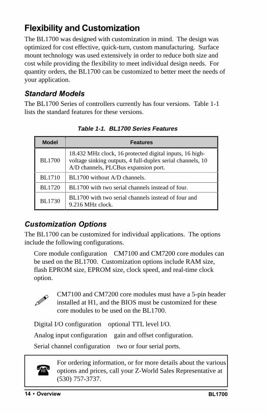
Flexibility and CustomizationThe BL1700 was designed with customization in mind. The design wasoptimized for cost effective, quick-turn, custom manufacturing. Surfacemount technology was used extensively in order to reduce both size andcost while providing the flexibility to meet individual design needs. Forquantity orders, the BL1700 can be customized to better meet the needs ofyour application.
Standard ModelsThe BL1700 Series of controllers currently has four versions. Table 1-1lists the standard features for these versions.
Customization OptionsThe BL1700 can be customized for individual applications. The optionsinclude the following configurations.
Core module configurationCM7100 and CM7200 core modules canbe used on the BL1700. Customization options include RAM size,flash EPROM size, EPROM size, clock speed, and real-time clockoption.
CM7100 and CM7200 core modules must have a 5-pin headerinstalled at H1, and the BIOS must be customized for thesecore modules to be used on the BL1700.
Digital I/O configurationoptional TTL level I/O.
Analog input configurationgain and offset configuration.
Serial channel configurationtwo or four serial ports.
For ordering information, or for more details about the variousoptions and prices, call your Z-World Sales Representative at(530) 757-3737.
Table 1-1. BL1700 Series Features
Model Features
BL170018.432 MHz clock, 16 protected digital inputs, 16 high-voltage sinking outputs, 4 full-duplex serial channels, 10A/D channels, PLCBus expansion port.
BL1710 BL1700 without A/D channels.
BL1720 BL1700 with two serial channels instead of four.
BL1730BL1700 with two serial channels instead of four and9.216 MHz clock.
!

BL1700 Overview s 15
Development and Evaluation ToolsThe BL1700 is supported by a Development Kit that includes everythingyou need to start development with the BLl700.
Development KitThe Development Kit includes these items.
Manual with schematics.
Programming cables and adapter.
24 V DC wall-mount power supply.
Field wiring terminals.
Sourcing high-voltage driver ICs.
An optional Serial Interface Board (SIB) allows full access to all serialports during development.
SoftwareThe BL1700 is programmed using Z-Worlds Dynamic C, an integrateddevelopment environment that includes an editor, a C compiler, and adebugger. Library functions provide an easy and robust interface to theBL1700.
Z-Worlds Dynamic C reference manuals provide completesoftware descriptions and programming instructions.$

BL170016 s Overview
CE ComplianceThe BL1700 has been tested by an approved competent body,and was found to be in conformity with applicable EN andequivalent standards. Note the following requirements forincorporating the BL1700 in your application to comply withCE requirements.
The power supply provided with the Development Kit is for develop-ment purposes only. It is the customers responsibility to provide aclean DC supply to the controller for all applications in end-products.
Fast transients/burst tests were not performed on the BL1700. Signaland process lines that are longer than 3 m should be routed in aseparate shielded conduit.
The BL1700 has been tested to Light Industrial Immunity standards.Additional shielding or filtering may be required for an industrialenvironment.
The BL1700 has been tested to EN55022 Class A emission standards.Additional shielding or filtering may be required to meet Class Bemission standards.
Visit the Technical Reference pages of the Z-World Web siteat http://www.zworld.com for more information on shieldingand filtering.
$
BL1700 Getting Started s 17
CHAPTER 2: GETTING STARTED
Chapter 2 provides instructions for connecting the BL1700 to a host PCand running a sample program. The following sections are included.
Development Kit Packing List
Connecting the BL1700 to Your PC
Establishing Communication with the BL1700
Running a Sample Program
BL170018 s Getting Started
(
Development Kit Packing ListThe BL1700 Development Kit includes the following items.
Two serial cables with DB-9 and 10-pin header connectors.
DB-25 to DB-9 serial adapter.
24 V DC wall-mount power transformer.
Two FWT-50 field wiring terminals.
One FWT-A/D field wiring terminal.
Two 2985 high-voltage driver ICs.
BL1700 Users Manual (this document).
Connecting the BL1700 to a Host PCThe BL1700 can be programmed using a PC through an RS-232 port withthe programming cable provided in the Developers Kit. You can also useZ-Worlds SIB2 to program the BL1700. Using the SIB2 frees all of theserial channels for the application during development. The SIB2 is notpart of the standard Developers Kit, and must be purchased separately.Both programming methods are described below.
For ordering information, call your Z-World Sales

BL1700 Getting Started s 19
Connecting the BL1700 to a PC using the serial port.
1. Make sure that Dynamic C is installed on your system as described inthe Dynamic C Technical Reference manual.
2. Connect the 10-pin programming cable from H12 on the BL1700 to theappropriate COM port of your computer as shown in Figure 2-1. Makesure that pin 1 on the ribbon cable connector (indicated by a smalltriangle on the connector) matches up with pin 1 on H12 (indicated bya small white circle near the corner of the connector).
Figure 2-1. BL1700 Programming Connections
Use only the transformer and programming cable suppliedby Z-World.
3. Make sure that the Run/Program jumper on header H4 is installed.
4. Connect the 24 V DC transformer as follows.
Connect the lead with the red sleeve to the screw terminal (J1)labeled DCIN on the BL1700.
Connect the other lead to the screw terminal (J1) labeled GND.
5. Plug the transformer into a wall socket.
9-pin
to PCBL1700
H12J1
BL170020 s Getting Started
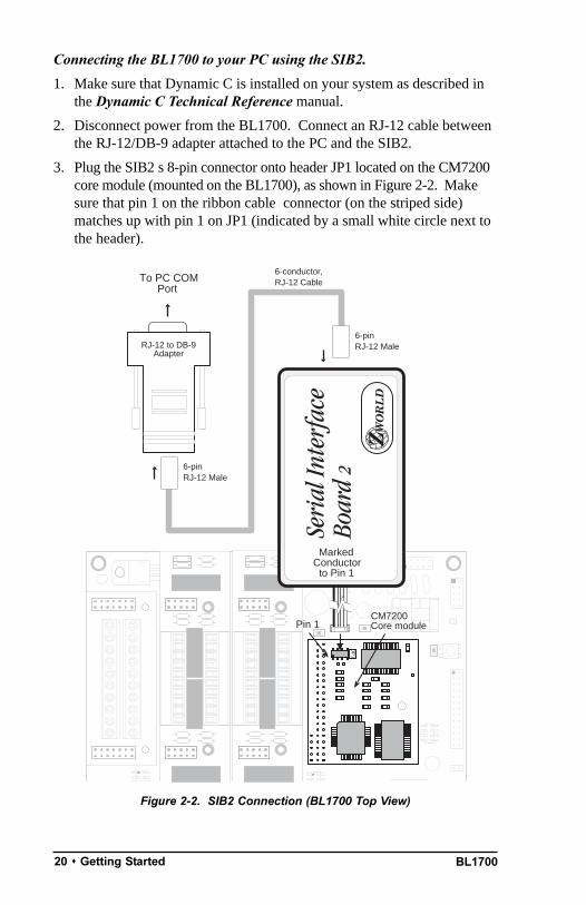
Connecting the BL1700 to your PC using the SIB2.
1. Make sure that Dynamic C is installed on your system as described inthe Dynamic C Technical Reference manual.
2. Disconnect power from the BL1700. Connect an RJ-12 cable betweenthe RJ-12/DB-9 adapter attached to the PC and the SIB2.
3. Plug the SIB2s 8-pin connector onto header JP1 located on the CM7200core module (mounted on the BL1700), as shown in Figure 2-2. Makesure that pin 1 on the ribbon cable connector (on the striped side)matches up with pin 1 on JP1 (indicated by a small white circle next tothe header).
Figure 2-2. SIB2 Connection (BL1700 Top View)
MarkedConductor to Pin 1
Pin 1
6-conductor,RJ-12 Cable
CM7200Core module
RJ-12 to DB-9Adapter
To PC COMPort
6-pinRJ-12 Male
6-pinRJ-12 Male
JP1
BL1700 Getting Started s 21
$
Use only the transformer and programming cable suppliedby Z-World.
Observe the polarity of the cable and the 8-pin connector.Attach the connector to JP1 exactly as shown in Figure 2-2.
4. Make sure that the Run/Program jumper on header H4 is installed.
5. Connect the 24 V DC transformer as follows.
Connect the lead with the red sleeve to the screw terminal (J1)labeled DCIN on the BL1700.
Connect the other lead to the screw terminal (J1) labeled GND.
6. Plug the power supply into a wall socket.
Establishing Communication with the BL17001. Double-click the Dynamic C icon to start the software. Note that
communication with the BL1700 is attempted each time you startDynamic C.
2. If the communication attempt is successful, no error messages aredisplayed.
See Appendix A, Troubleshooting, if an error message suchas Target Not Responding or Communication Error appears.
Once the necessary changes have been made to establish com-munication between the host PC and the BL1700, use theDynamic C shortcut <Ctrl Y> to reset the controller and initiatecommunication.
!

BL170022 s Getting Started
Running a Sample Program1. Open the sample program BL17FLSH.C located in the Dynamic C
SAMPLES\BL17XX directory. This program flashes the onboard LED.
2. Compile the program by pressing F3 or by choosing Compile from theCompile menu. Dynamic C compiles and downloads the program intothe BL1700s flash memory.
During compilation, Dynamic C rapidly displays several messages inthe compiling window. This condition is normal.
See Appendix A, Troubleshooting, if an error message suchas Target Not Responding or Communication Error appears.
3. Run the program by pressing F9 or by choosing Run from the RunMenu.
4. To halt the program, press <Ctrl Z>. This action halts programexecution.
5. To restart program execution, when required, press F9.
$

BL1700 BL1700 Hardware s 23
CHAPTER 3: BL1700 HARDWARE
Chapter 3 describes the BL1700 hardware subsystems. The followingsections are included.
Operating Modes
BL1700 Subsystems Overview
Microprocessor Core Module
Serial Communications Channels
High-Voltage Digital Outputs
Protected Digital Inputs
Analog Inputs
PLCBus Expansion Port

BL170024 s BL1700 Hardware
Operating ModesThe BL1700 has two mutually exclusive operating modes, run mode andprogram mode. Each mode is explained in detail below.
Program Mode
In program mode, the BL1700 controller runs under the control of yourPC that is running Dynamic C. The BL1700 must be in this mode tocompile a program to the BL1700 or debug a program.
In program mode, the BL1700 matches the baud rate of thePC COM port up to 57,600 bps.
USER LED is ON in program mode.
Run Mode
In run mode, the BL1700 controller runs standalone. At power-up, theBL1700 checks to see if its onboard memory contains a program. If aprogram exists, the BL1700 controller executes the program immedi-ately after power-up.
In run mode, the BL1700 does not respond to Dynamic Crunning on the PC. A program cannot be compiled ordebugged when the BL1700 is in run mode.
USER LED D2 is under the control of the application onthe BL1700 when the BL1700 is in run mode.
Table 3-1 shows the jumper settings for the program and run modes.
!
!
Table 3-1. BL1700 Jumper Settings for Run/Program Modes
OperatingMode
HeaderH4 Permissible Activities
ProgramMode
• Compile a program.
• Run a program under debugger control.
• Run a program without “polling.” See yourDynamic C manuals for a description ofprogram polling.
Run Mode Run application.
H4
H4
BL1700 BL1700 Hardware s 25
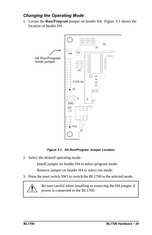
Changing the Operating Mode1. Locate the Run/Program jumper on header H4. Figure 3-1 shows the
location of header H4.
Figure 3-1. H4 Run/Program Jumper Location
2. Select the desired operating mode.
Install jumper on header H4 to select program mode.
Remove jumper on header H4 to select run mode.
3. Press the reset switch SW1 to switch the BL1700 to the selected mode.
Be sure careful when installing or removing the H4 jumper ifpower is connected to the BL1700.
0.125 dia
H1
J5
H4 C1
J4
U2
D1
U13
U14
J6
U20
MV1 MV2 MV3 MV4 MV5 MV6
C7L1
J7
C6
RN1
H12
J1
SW1
D2
R13
C2
R1
C4
R8
R9
R3
R6
R7
C5
R4
R5
R10
R2C3
C1
H4 Run/Programmode jumper
BL170026 s BL1700 Hardware
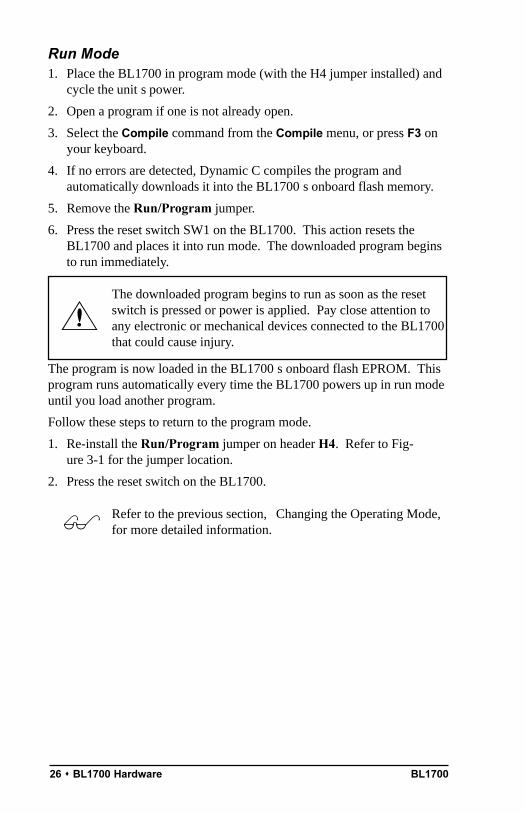
Run Mode1. Place the BL1700 in program mode (with the H4 jumper installed) and
cycle the units power.
2. Open a program if one is not already open.
3. Select the Compile command from the Compile menu, or press F3 onyour keyboard.
4. If no errors are detected, Dynamic C compiles the program andautomatically downloads it into the BL1700s onboard flash memory.
5. Remove the Run/Program jumper.
6. Press the reset switch SW1 on the BL1700. This action resets theBL1700 and places it into run mode. The downloaded program beginsto run immediately.
The downloaded program begins to run as soon as the resetswitch is pressed or power is applied. Pay close attention toany electronic or mechanical devices connected to the BL1700that could cause injury.
The program is now loaded in the BL1700s onboard flash EPROM. Thisprogram runs automatically every time the BL1700 powers up in run modeuntil you load another program.
Follow these steps to return to the program mode.
1. Re-install the Run/Program jumper on header H4. Refer to Fig-ure 3-1 for the jumper location.
2. Press the reset switch on the BL1700.
Refer to the previous section, Changing the Operating Mode,for more detailed information.$
BL1700 BL1700 Hardware s 27
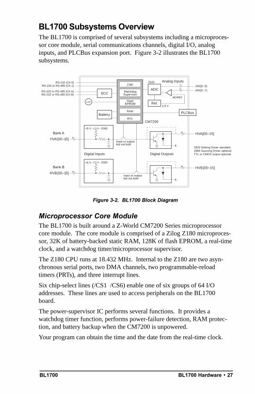
BL1700 Subsystems OverviewThe BL1700 is comprised of several subsystems including a microproces-sor core module, serial communications channels, digital I/O, analoginputs, and PLCBus expansion port. Figure 3-2 illustrates the BL1700subsystems.
Figure 3-2. BL1700 Block Diagram
Microprocessor Core ModuleThe BL1700 is built around a Z-World CM7200 Series microprocessorcore module. The core module is comprised of a Zilog Z180 microproces-sor, 32K of battery-backed static RAM, 128K of flash EPROM, a real-timeclock, and a watchdog timer/microprocessor supervisor.
The Z180 CPU runs at 18.432 MHz. Internal to the Z180 are two asyn-chronous serial ports, two DMA channels, two programmable-reloadtimers (PRTs), and three interrupt lines.
Six chip-select lines (/CS1/CS6) enable one of six groups of 64 I/Oaddresses. These lines are used to access peripherals on the BL1700board.
The power-supervisor IC performs several functions. It provides awatchdog timer function, performs power-failure detection, RAM protec-tion, and battery backup when the CM7200 is unpowered.
Your program can obtain the time and the date from the real-time clock.
2
RS-232 or RS-485 (Ch A)
HVA[00–15]
Z180
PLCBus
Digital Inputs
K
CM7200
SCCRS-232 or RS-485 (Ch B)
HVB[00–15]
K
16
16
2803 Sinking Driver standard2985 Sourcing Driver optionalTTL or CMOS output optional
HVB[00–15]
GND
HVA[00–15]
GND
AIN[0–7]
ADREF
2543
ADCAIN[8–9]
Ref.
8
Input or outputbut not both
Input or outputbut not both
16
16
BatteryRAM
RTC
RS-232 or RS-485 (Ch 1)RS-232 (Ch 0)
Digital Outputs
Analog Inputs
LED
2.5 V
FlashEPROM
WatchdogSupervisor
+5 V
+5 V
Bank A
Bank B
BL170028 s BL1700 Hardware
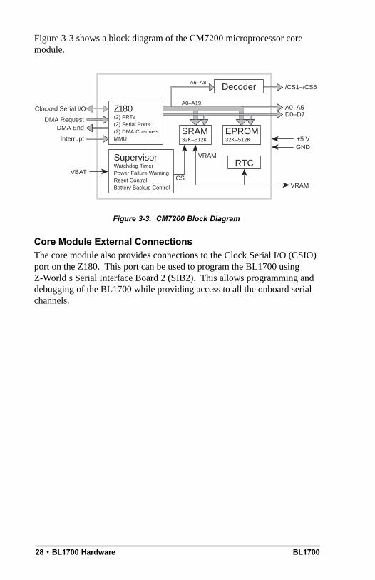
Figure 3-3 shows a block diagram of the CM7200 microprocessor coremodule.
Figure 3-3. CM7200 Block Diagram
Core Module External ConnectionsThe core module also provides connections to the Clock Serial I/O (CSIO)port on the Z180. This port can be used to program the BL1700 usingZ-Worlds Serial Interface Board 2 (SIB2). This allows programming anddebugging of the BL1700 while providing access to all the onboard serialchannels.
DMA Request
A0–A5D0–D7
/CS1–/CS6
VBAT
GND
VRAM
Interrupt
A0–A19
A6–A8
CS
DMA End
Decoder
EPROM32K–512K
SRAM32K–512K
RTC
Z180(2) PRTs(2) Serial Ports(2) DMA ChannelsMMU
SupervisorWatchdog TimerPower Failure WarningReset ControlBattery Backup Control
VRAM
+5 V
Clocked Serial I/O
BL1700 BL1700 Hardware s 29
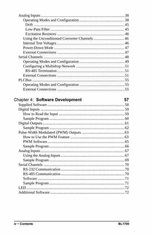
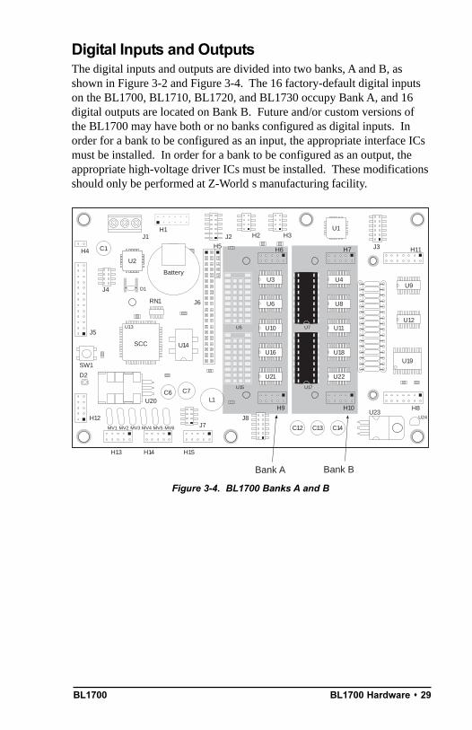
Digital Inputs and OutputsThe digital inputs and outputs are divided into two banks, A and B, asshown in Figure 3-2 and Figure 3-4. The 16 factory-default digital inputson the BL1700, BL1710, BL1720, and BL1730 occupy Bank A, and 16digital outputs are located on Bank B. Future and/or custom versions ofthe BL1700 may have both or no banks configured as digital inputs. Inorder for a bank to be configured as an input, the appropriate interface ICsmust be installed. In order for a bank to be configured as an output, theappropriate high-voltage driver ICs must be installed. These modificationsshould only be performed at Z-Worlds manufacturing facility.
Figure 3-4. BL1700 Banks A and B
Battery
SCC
Bank A Bank B
H11
H1
J5
H4 C1
J4
U2
D1
U13
U14
J6
H5
U20
MV1 MV2 MV3 MV4 MV5 MV6
C7
H13 H14 H15
J8
L1
J7
C6
C12 C13 C14
J3
H3H2J2
RN1
H12
J1
SW1
D2
U9
U12
U19
U4
U8
U11
U18
U22
H10 H8U24
U23
U17
U7
H9
H6 H7
U5
U1
U3
U6
U10
U16
U21
U15
BL170030 s BL1700 Hardware
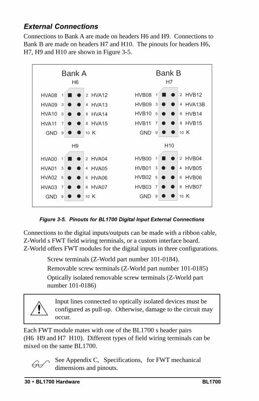
External ConnectionsConnections to Bank A are made on headers H6 and H9. Connections toBank B are made on headers H7 and H10. The pinouts for headers H6,H7, H9 and H10 are shown in Figure 3-5.
Figure 3-5. Pinouts for BL1700 Digital Input External Connections
Connections to the digital inputs/outputs can be made with a ribbon cable,Z-Worlds FWT field wiring terminals, or a custom interface board.Z-World offers FWT modules for the digital inputs in three configurations.
Screw terminals (Z-World part number 101-0184). Removable screw terminals (Z-World part number 101-0185) Optically isolated removable screw terminals (Z-World part
number 101-0186)
Input lines connected to optically isolated devices must beconfigured as pull-up. Otherwise, damage to the circuit mayoccur.
Each FWT module mates with one of the BL1700s header pairs(H6H9 and H7H10). Different types of field wiring terminals can bemixed on the same BL1700.
See Appendix C, Specifications, for FWT mechanicaldimensions and pinouts.
10
H6
1 2
3 4
5 6
7 8
9
HVA08
HVA09
HVA10
HVA11
GND
HVA12
HVA13
HVA14
HVA15
K
10
H9
1 2
3 4
5 6
7 8
9
HVA00
HVA01
HVA02
HVA03
GND
HVA04
HVA05
HVA06
HVA07
K
10
H7
1 2
3 4
5 6
7 8
9
HVB08
HVB09
HVB10
HVB11
GND
HVB12
HVA13B
HVB14
HVB15
K
10
H10
1 2
3 4
5 6
7 8
9
HVB00
HVB01
HVB02
HVB03
GND
HVB04
HVB05
HVB06
HVB07
K
Bank A Bank B
$
BL1700 BL1700 Hardware s 31
Digital InputsThe BL1700 can provide up to 32 protected digital inputs designed aslogical data inputs, returning a 1 or 0. Their normal operating range is-20 V DC to +24 V DC, and they are protected from voltages between-48 V DC and +48 V DC. The inputs can detect logic-level signals andhave a nominal logic threshold of 2.5 V DC. This means an input returns a0 if the input voltage is below 2.5 V DC and a 1 if the input voltage isabove 2.5 V DC. The inputs can be pulled up to +5 V or down to ground.
A low-pass filter on each input channel has a time constant of
TRC
= 220 µs (4.5 kHz).
They may be configured as pull-up or pull-down in groups of fours andeights. The configuration of each input should be determined by normaloperating conditions, power-down mode and possible failure modesincluding open or shorted conditions. These factors will influence yourdecision about configuring the inputs as pull-up or pull-down.
Operating Modes and ConfigurationInputs may be pulled up to +5 V or pulled down to ground by configuringthe jumpers on BL1700 headers J2 and J3.
J2 jumpers select pull-up/pull-down resistors for Bank A. Jumpers on J3select pull-up/pull-down resistors for inputs for Bank B. To change aninput from the factory default of pull-up, simply place a jumper across theappropriate two pins of J2 and/or J3.
Table 3-2 and Table 3-3 illustrate the jumper settings for pull-up and pull-down configurations for the BL1700s Bank A and Bank B inputs.
The factory default is for the digital inputs to be pulled up to+5 V.FD

BL170032 s BL1700 Hardware
Table 3-2. BL1700 Bank A Digital Input Jumper Configurations
Jumper SettingsChannel
Inputs Pulled Up Inputs Pulled Down
HVA 0–3
Bank AChannels8–11
(PhysicalChannels24–27)
HVA 4–7
Bank AChannels12–15
(PhysicalChannels28–31)
HVA 8–15
Bank AChannels0–7
(PhysicalChannels16–23)
10
12
J2
1 2
3 4
5 6
7 8
9
11
FD
10
12
J2
1 2
3 4
5 6
7 8
9
11
FD
10
12
J2
1 2
3 4
5 6
7 8
9
11
FD
10
12
J2
1 2
3 4
5 6
7 8
9
11
10
12
J2
1 2
3 4
5 6
7 8
9
11
10
12
J2
1 2
3 4
5 6
7 8
9
11
BL1700 BL1700 Hardware s 33
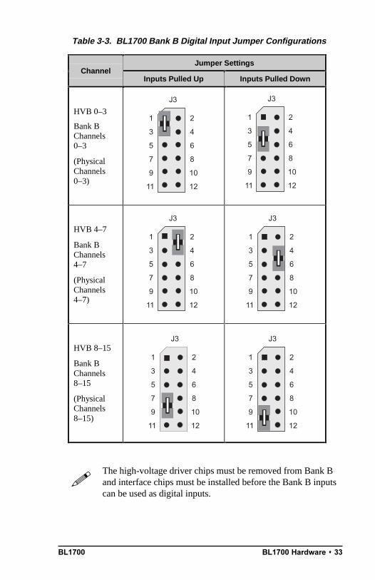
The high-voltage driver chips must be removed from Bank Band interface chips must be installed before the Bank B inputscan be used as digital inputs.
Table 3-3. BL1700 Bank B Digital Input Jumper Configurations
Jumper SettingsChannel
Inputs Pulled Up Inputs Pulled Down
HVB 0–3
Bank BChannels0–3
(PhysicalChannels0–3)
HVB 4–7
Bank BChannels4–7
(PhysicalChannels4–7)
HVB 8–15
Bank BChannels8–15
(PhysicalChannels8–15)
10
12
J3
1 2
3 4
5 6
7 8
9
11
10
12
J3
1 2
3 4
5 6
7 8
9
11
10
12
J3
1 2
3 4
5 6
7 8
9
11
10
12
J3
1 2
3 4
5 6
7 8
9
11
10
12
J3
1 2
3 4
5 6
7 8
9
11
10
12
J3
1 2
3 4
5 6
7 8
9
11
!
BL170034 s BL1700 Hardware
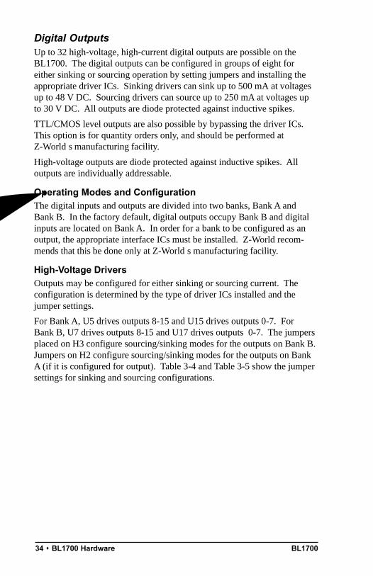
Digital OutputsUp to 32 high-voltage, high-current digital outputs are possible on theBL1700. The digital outputs can be configured in groups of eight foreither sinking or sourcing operation by setting jumpers and installing theappropriate driver ICs. Sinking drivers can sink up to 500 mA at voltagesup to 48 V DC. Sourcing drivers can source up to 250 mA at voltages upto 30 V DC. All outputs are diode protected against inductive spikes.
TTL/CMOS level outputs are also possible by bypassing the driver ICs.This option is for quantity orders only, and should be performed atZ-Worlds manufacturing facility.
High-voltage outputs are diode protected against inductive spikes. Alloutputs are individually addressable.
Operating Modes and ConfigurationThe digital inputs and outputs are divided into two banks, Bank A andBank B. In the factory default, digital outputs occupy Bank B and digitalinputs are located on Bank A. In order for a bank to be configured as anoutput, the appropriate interface ICs must be installed. Z-World recom-mends that this be done only at Z-Worlds manufacturing facility.
High-Voltage DriversOutputs may be configured for either sinking or sourcing current. Theconfiguration is determined by the type of driver ICs installed and thejumper settings.
For Bank A, U5 drives outputs 8-15 and U15 drives outputs 0-7. ForBank B, U7 drives outputs 8-15 and U17 drives outputs 0-7. The jumpersplaced on H3 configure sourcing/sinking modes for the outputs on Bank B.Jumpers on H2 configure sourcing/sinking modes for the outputs on BankA (if it is configured for output). Table 3-4 and Table 3-5 show the jumpersettings for sinking and sourcing configurations.
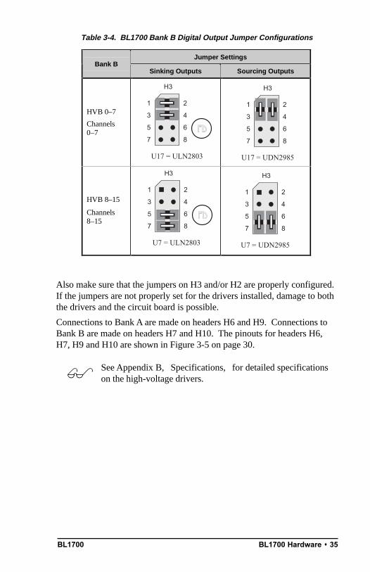
BL1700 BL1700 Hardware s 35
Also make sure that the jumpers on H3 and/or H2 are properly configured.If the jumpers are not properly set for the drivers installed, damage to boththe drivers and the circuit board is possible.
Connections to Bank A are made on headers H6 and H9. Connections toBank B are made on headers H7 and H10. The pinouts for headers H6,H7, H9 and H10 are shown in Figure 3-5 on page 30.
See Appendix B, Specifications, for detailed specificationson the high-voltage drivers.
Table 3-4. BL1700 Bank B Digital Output Jumper Configurations
Jumper SettingsBank B
Sinking Outputs Sourcing Outputs
HVB 0–7
Channels0–7
HVB 8–15
Channels8–15
H3
1 2
3 4
5 6
7 8
U17 = ULN2803
FD
H3
1 2
3 4
5 6
7 8
U17 = UDN2985
H3
1 2
3 4
5 6
7 8
U7 = ULN2803
FD
H3
1 2
3 4
5 6
7 8
U7 = UDN2985
$

BL170036 s BL1700 Hardware
The digital interface chips must be removed from Bank A andhigh-voltage driver chips must be installed before the Bank Ainputs can be used as outputs.
Table 3-5. BL1700 Bank A Digital Output Jumper Configurations
Jumper SettingsBank A
Sinking Outputs Sourcing Outputs
HVA 0–7
Channels8–15
HVA 8–15
Channels0–7
H2
1 2
3 4
5 6
7 8
U5 = ULN2803
H2
1 2
3 4
5 6
7 8
U5 = UDN2985
H2
1 2
3 4
5 6
7 8
U15 = ULN2803
H2
1 2
3 4
5 6
7 8
U15 = UDN2985
!
BL1700 BL1700 Hardware s 37
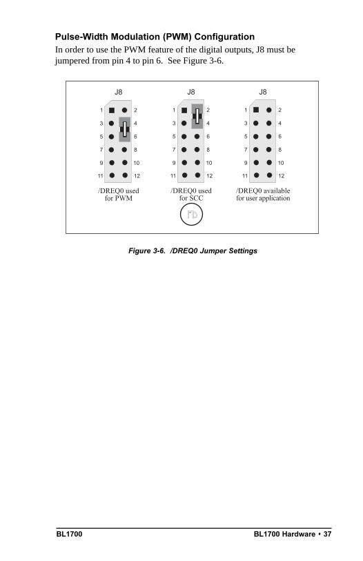
Pulse-Width Modulation (PWM) ConfigurationIn order to use the PWM feature of the digital outputs, J8 must bejumpered from pin 4 to pin 6. See Figure 3-6.
Figure 3-6. /DREQ0 Jumper Settings
10
J8
1 2
3 4
5 6
7 8
9
1211
/DREQ0 usedfor PWM
10
J8
1 2
3 4
5 6
7 8
9
1211
/DREQ0 usedfor SCC
10
J8
1 2
3 4
5 6
7 8
9
1211
/DREQ0 availablefor user application
FD
BL170038 s BL1700 Hardware
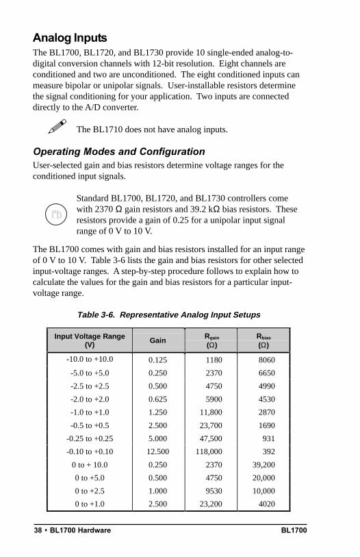
Analog InputsThe BL1700, BL1720, and BL1730 provide 10 single-ended analog-to-digital conversion channels with 12-bit resolution. Eight channels areconditioned and two are unconditioned. The eight conditioned inputs canmeasure bipolar or unipolar signals. User-installable resistors determinethe signal conditioning for your application. Two inputs are connecteddirectly to the A/D converter.
The BL1710 does not have analog inputs.
Operating Modes and ConfigurationUser-selected gain and bias resistors determine voltage ranges for theconditioned input signals.
Standard BL1700, BL1720, and BL1730 controllers comewith 2370 Ω gain resistors and 39.2 kΩ bias resistors. Theseresistors provide a gain of 0.25 for a unipolar input signalrange of 0 V to 10 V.
The BL1700 comes with gain and bias resistors installed for an input rangeof 0 V to 10 V. Table 3-6 lists the gain and bias resistors for other selectedinput-voltage ranges. A step-by-step procedure follows to explain how tocalculate the values for the gain and bias resistors for a particular input-voltage range.
!
FD
Table 3-6. Representative Analog Input Setups
Input Voltage Range(V) Gain
Rgain
(Ω)Rbias
(Ω)
-10.0 to +10.0 0.125 1180 8060
-5.0 to +5.0 0.250 2370 6650
-2.5 to +2.5 0.500 4750 4990
-2.0 to +2.0 0.625 5900 4530
-1.0 to +1.0 1.250 11,800 2870
-0.5 to +0.5 2.500 23,700 1690
-0.25 to +0.25 5.000 47,500 931
-0.10 to +0.10 12.500 118,000 392
0 to + 10.0 0.250 2370 39,200
0 to +5.0 0.500 4750 20,000
0 to +2.5 1.000 9530 10,000
0 to +1.0 2.500 23,200 4020
BL1700 BL1700 Hardware s 39
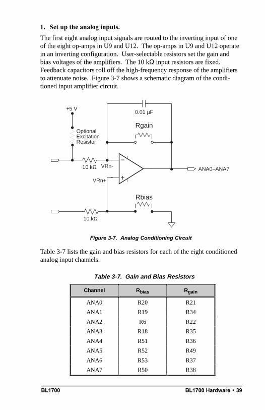
1. Set up the analog inputs.
The first eight analog input signals are routed to the inverting input of oneof the eight op-amps in U9 and U12. The op-amps in U9 and U12 operatein an inverting configuration. User-selectable resistors set the gain andbias voltages of the amplifiers. The 10 kΩ input resistors are fixed.Feedback capacitors roll off the high-frequency response of the amplifiersto attenuate noise. Figure 3-7 shows a schematic diagram of the condi-tioned input amplifier circuit.
Figure 3-7. Analog Conditioning Circuit
Table 3-7 lists the gain and bias resistors for each of the eight conditionedanalog input channels.
ANA0–ANA7+
–
10 kΩ
10 kΩ
0.01 µF
Rgain
Rbias
VRn+
VRn-
OptionalExcitationResistor
+5 V
Table 3-7. Gain and Bias Resistors
Channel Rbias Rgain
ANA0 R20 R21
ANA1 R19 R34
ANA2 R6 R22
ANA3 R18 R35
ANA4 R51 R36
ANA5 R52 R49
ANA6 R53 R37
ANA7 R50 R38
BL170040 s BL1700 Hardware
(
Strip sockets spaced 0.400 inches (10.2 mm) apart accommodate the gainand bias resistors.
Z-World can install surface-mounted excitation, gain and biasresistors for your exact configuration in production quantities.For more information, call your Z-World Sales Representativeat (530) 757-3737.
2. Select gain resistor.
The gain and bias resistors determine the input signals voltage relative toground as well as its range. For example, assume your circuit must handlean input signal voltage range of 10 V spanning -5 V to +5 V. You shouldfirst select the gain (feedback) resistor to suit an input signal voltage rangeof 10 V.
The gain of the amplifier is the ratio of its maximum output-voltage swingto your applications maximum input-voltage swing. The 2.5 V input-voltage range of the A/D chip limits the op-amps output swing to 2.5 V.Therefore, Equation (3-1) expresses an amplifiers gain in terms of itsinput-voltage range.
where g is the gain, VINmax is the maximum input voltage and VINmin
is theminimum input voltage.
The ratio of the user-specified gain resistor Rgain
to its associated fixedinput resistor determines an amplifiers gain. For the amplifier in Fig-ure 3-7 with its input resistor fixed at 10 kΩ, the gain is
Given an input voltage range of 10 V, this gain equation fixes theamplifiers gain at 0.25. This gain scales the input signals range properlydown to the op-amps 2.5 V maximum output range. R
gain must therefore
be 2500 Ω.
3. Determine bias resistor.
If the op-amp is to servo its output properly around the desired centervoltage, you must establish the appropriate bias voltage at the op-ampsnoninverting input. You must select the bias, or offset, resistor, R
bias, to
position the input-voltage range correctly with respect to ground. For thisexample, let us use -5 V to +5 V.
minmax ININ VV
V2.5g
−= (3-1)
.10,000
Rg
gain
Ω= (3-2)
BL1700 BL1700 Hardware s 41
Because the value for Rgain
has already been selected, the maximum inputvoltage, V
INmax, determines the maximum voltage seen at the amplifiers
summing junction (inverting input)circuit nodes VR0 through VR7.Compute VR0 through VR7 using Equation (3-3).
For each op-amp, the bias voltage, Vbias, must equal its correspondingVRn. A voltage divider, comprising a bias resistor and a fixed 10 kΩresistor, derive the bias voltage from VREF+. Note that VREF+ is notnecessarily the same as REF+. REF+ is the positive reference voltage theA/D chip uses.
VREF+ is 2.5 V and Rbias
is
Continuing the example for an input-voltage range that necessitates a gainof 0.25, and for which V
MAX is +5 V, V
bias is then 1.0 V. Therefore, R
bias is
6667 Ω in absolute mode.
Now suppose that the input range is 0 V to +10 V instead of 5 V to +5 V.V
max is now +10 V and V
bias becomes 2.0 V. R
bias is then 40 kΩ.
4. Choose resistor values.
The calculated values, of course, will not always be available as standardresistor values. In these cases, use the nearest standard resistor value. Forexample, rather than 6667 Ω, use 6650 Ω if you are using 1% resistors, oruse 6800 Ω if you are using 5% resistors.
5. Bracket input range.
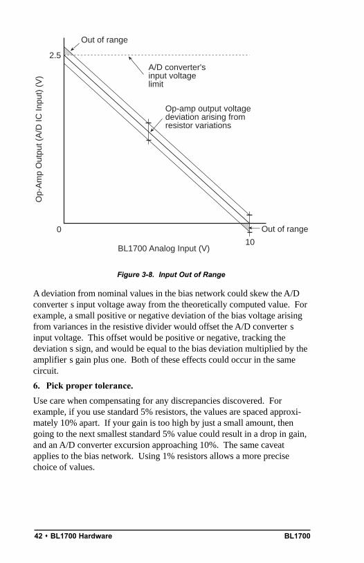
To be sure of accurately measuring signals at the extremes of an inputrange, you must be aware of the interaction between the 10 kΩ fixedresistors and the resistors you install. In the ideal case, if you were tomeasure a signal at the minimum input level, the A/D converters inputwould be at the maximum expected value of 2.5 V.
However, in the real world, resistor values vary within their rated tolerancebands. Thus, if the fixed input resistor is lower than its nominal value, andthe installed resistor is slightly higher than its nominal value, the actualinput to the A/D converter would be greater than 2.5 V. A loss of accuracythen results because the A/D converter input would reach its maximuminput value before the true signal input reaches the minimum expectedinput level, as shown in Figure 3-8.
+
×=g1
gVVR0
maxIN (3-3)
.V-V
000,10VR
bias
biasbias 2.5
Ω×= (3-4)
BL170042 s BL1700 Hardware
Figure 3-8. Input Out of Range
A deviation from nominal values in the bias network could skew the A/Dconverters input voltage away from the theoretically computed value. Forexample, a small positive or negative deviation of the bias voltage arisingfrom variances in the resistive divider would offset the A/D convertersinput voltage. This offset would be positive or negative, tracking thedeviations sign, and would be equal to the bias deviation multiplied by theamplifiers gain plus one. Both of these effects could occur in the samecircuit.
6. Pick proper tolerance.
Use care when compensating for any discrepancies discovered. Forexample, if you use standard 5% resistors, the values are spaced approxi-mately 10% apart. If your gain is too high by just a small amount, thengoing to the next smallest standard 5% value could result in a drop in gain,and an A/D converter excursion approaching 10%. The same caveatapplies to the bias network. Using 1% resistors allows a more precisechoice of values.
0
10
2.5
BL1700 Analog Input (V)
Op-
Am
p O
utpu
t (A
/D IC
Inpu
t) (
V)
A/D converter'sinput voltagelimit
Op-amp output voltagedeviation arising fromresistor variations
Out of range
Out of range
BL1700 BL1700 Hardware s 43
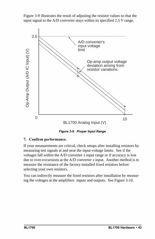
Figure 3-9 illustrates the result of adjusting the resistor values so that theinput signal to the A/D converter stays within its specified 2.5 V range.
Figure 3-9. Proper Input Range
7. Confirm performance.
If your measurements are critical, check setups after installing resistors bymeasuring test signals at and near the input-voltage limits. See if thevoltages fall within the A/D converters input range or if accuracy is lostdue to over-excursions at the A/D converters input. Another method is tomeasure the resistance of the factory-installed fixed resistors beforeselecting your own resistors.
You can indirectly measure the fixed resistors after installation by measur-ing the voltages at the amplifiers inputs and outputs. See Figure 3-10.
0 10
2.5
BL1700 Analog Input (V)
Op-
Am
p O
utpu
t (A
/D IC
Inpu
t) (
V)
A/D converter'sinput voltagelimit
Op-amp output voltagedeviation arising fromresistor variations

BL170044 s BL1700 Hardware
Figure 3-10. Signal Conditioning Test Points
Using Channel 0 as an example, ground the input A0 at pin 1 of H11.Then measure the voltages at VR0- and the amplifiers output. Becausethe currents through the input resistor and the feedback resistor areessentially identical, the ratio of the voltages across the resistors isequivalent to the ratio of the resistors. Therefore, the gain is
Again using Channel 0 as an example, measure the voltage of VREF andthe voltage at VR0+. Because the current into the op-amp input is negli-gible, the resistance ratio of the two resistors in the voltage divider alonedetermines VR0+. You can then compute the value of the fixed resistor inthe divider once you know both the value of the resistor you installed andthe value of VR0+.
8. Calibrate the BL1700 A/D converter.
Mathematically derived values provide good baseline gain values. Cali-bration is necessary because the inherent component-to-componentvariations of resistors can completely swamp the 0.25% resolution of theA/D converter. To achieve the highest accuracy possible, calibrate theBL1700.
ANA0–ANA7+
–10 kΩ
0.01 µF
Rgain
Rbias
VRn+
VRn-
VREF
VOUT
+5 V
.-VR0
-VR0-VOUTgain = (3-5)
BL1700 BL1700 Hardware s 45
Dynamic C provides a routine to compute calibration coefficients and storethe coefficients in nonvolatile memory. The routine uses two referencepoints to compute the coefficients. Each reference point comprises a pairof values: the actual applied test voltage and raw converted A/D value (a12-bit integer). The supplied Z-World A/D software will automatically usethese calibration coefficients to correct all subsequent A/D readings.
The factory installed fixed resistors have a 1% tolerance.
Calibration constants for the factory installed resistors are stored insimulated EEPROM during testing.
9. Recalibrate the BL1700.
To recalibrate a BL1700, apply two known test voltages to each channelyou plan to use. Get the converted reading for each test voltage and passthem, along with the test voltages, to the function eioBrdACalib tocalculate the conversion coefficients for that channel. eioBrdACalib willautomatically store the coefficients in the flash EPROM.
Sample program BL17AIN.C in the Dynamic C SAMPLES directory showshow to calibrate the conditioned analog input channels of a BL1700 manu-ally, assuming test voltages of 1.00 V and 9.00 V.
DriftThe AD680JT voltage reference displays a voltage drift of 10 ppm/°C(typ) to 30 ppm/°C (max). This drift corresponds to 25 mV/°C to75 mV/°C, or 1.75 mV to 5.25 mV over the temperature range of 0°C to70°C.
The LMC660C operational amplifier exhibits an offset-voltage drift of1.3 µV/°C (typ), or 91 mV over the operating temperature range.
Low-Pass FilterThe 0.01 mF feedback capacitors in the amplifier’s feedback path trans-form the amplifiers into low-pass filters. These filters attenuate any high-frequency noise that may be present in your signal. These filters’ charac-teristics depend on the resistors your select.
The 3 dB corner frequency of a filter is
For the case above with a gain of 0.25 using a 1% feedback resistor of2490 Ω, the 3 dB corner frequency is 6392 Hz.
.F0.01R2
1f
gdb3 µπ ××
= (3-6)
BL170046 s BL1700 Hardware
Excitation ResistorsSome transducers require an excitation voltage. For example, a thermistor,serving as one leg of a voltage divider (having a fixed resistor in the otherleg), measures temperature. The voltage at the dividers junction will varywith temperature. There is provision for excitation resistors to be installedon the inputs of the eight conditioned analog channels. The excitationresistors are tied to the +5 V analog supply.
Using the Unconditioned Converter ChannelsThe eight conditioned channels use the first eight channels, AIN0AIN7,of the A/D converter chip. Two additional channels are also available.You can access these channels with software by inserting your desiredchannel number in the library functions that control the BL1700. Thesesignals are available on headers H8 and H11.
For optimum results, drive these channels with low output impedancevoltage sourcesless than 50 Ω. Op-amps are ideal for this purpose. Highoutput impedance sources, on the other hand, are susceptible to couplednoise. In addition, only a low-impedance source can quickly charge thesampling capacitors within the A/D converter. When designing the signalsources to drive the extra channels, be sure to consider whether theamplifiers you choose can handle the capacitance of the cable that con-nects to the analog input connectors.
Internal Test VoltagesIn addition to the external input channels of the A/D converter chip, threeadditional internal channels exist to measure reference points within the A/D converter chip. Unfortunately, the A/D converter compares its internalnodes to REF+ and REF- so the conversions yield either all 1s or all 0s.You may access these channels using ordinary library routines by specify-ing the appropriate channel address when calling the functions.
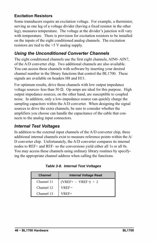
Table 3-8. Internal Test Voltages
Channel Internal Voltage Read
Channel 11 (VREF+ – VREF−) ÷ 2
Channel 12 VREF−
Channel 13 VREF+
BL1700 BL1700 Hardware s 47
Power-Down ModeIf you select Channel 14, the A/D converter chip enters a power-downmode in which all circuitry within the chip goes into a low-current, standbymode. Upon power-up and before the first conversion, the chip also goesinto the power-down mode. The chip remains in the power-down modeuntil you select a channel other than 14. The normal operating current ofthe A/D converter chip is 1 mA to 2.5 mA. In power-down mode thisconsumption is reduced to 4 µA to 25 µA.
External ConnectionsConnections to the analog inputs can be made with a ribbon cable,Z-Worlds FWT field wiring terminals, or a custom interface board.Z-World offers FWT modules for the digital inputs in three configurations.
Screw terminals (Z-World part number 101-0184). Removable screw terminals (Z-World part number 101-0185)
The FWT module mates with the BL1700s header pairs H8H11.
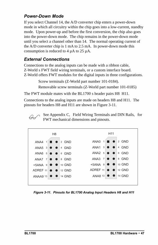
Connections to the analog inputs are made on headers H8 and H11. Thepinouts for headers H8 and H11 are shown in Figure 3-11.
See Appendix C, Field Wiring Terminals and DIN Rails, forFWT mechanical dimensions and pinouts.
Figure 3-11. Pinouts for BL1700 Analog Input Headers H8 and H11
$
10
H8
1 2
3 4
5 6
7 8
9
ANA4
ANA5
ANA6
ANA7
+5ANA
GND
GND
GND
GND
GND
14
11 12
13
ADREF
ANAA9
GND
GND
10
H11
1 2
3 4
5 6
7 8
9
ANA0
ANA1
ANA2
ANA3
+5ANA
GND
GND
GND
GND
GND
14
11 12
13
ADREF
ANA8
GND
GND
BL170048 s BL1700 Hardware
Serial ChannelsFour serial channels are available on the BL1700. One channel, Channel0, is a dedicated RS-232 communication channel. The other three areavailable in either RS-232 or RS-485 configurations. Channel 0 andChannel 1 are connected to the Z180s Serial Channel 0 and SerialChannel 1, respectively. Channel A and Channel B are controlled by theSerial Communications Controller (SCC) chip on the BL1700; these twoports also have hardware support for synchronous communication. Serialchannel signals are routed to either RS-232 or RS-485 converters viaconfiguration jumpers. Baud rates up to 57,600 bps are supported.
The BL1720 and BL1730 versions have two serial ports. The serial ports onthe BL1720BL1730 versions do not support synchronous communication.
Table 3-9 summarizes the operating modes for the four channels.
Channel 0Channel 0 is the BL1700s RS-232 programming port and is configured asthree-wire or five-wire RS-232. Channel 0 cannot be reconfigured.
Channel 1Channel 1 is a general-purpose serial channel that can be configured astwo-wire RS-485 or three-wire RS-232.
Channel AChannel A is a general-purpose serial channel controlled by a Zilog SerialCommunication Controller (SCC) chip on the BL1700. Channel A can beconfigured as two-wire RS-485 or five-wire RS-232. When configured asRS-232, Channel A also provides DCD and DTR signals. Synchronouscommunication is possible on this channel, but is not supported by DynamicC drivers at this time. Channel A is not available on the BL1720 or BL1730.
Channel BChannel B is a general-purpose serial channel. Along with Channel A, it iscontrolled by the Serial Communication Controller chip. Channel B can beconfigured as two-wire RS-485 or five-wire RS-232. Synchronous communi-cation is possible on this channel, but is not supported by Dynamic C driversat this time. Channel B is not available on the BL1720 or BL1730.
Table 3-9. Serial Channel Configuration Options
Channel Configurations
Channel 0 Three-wire or five-wire RS-232 only
Channel 1 Two-wire RS-485 or three-wire RS-232
Channel A Two-wire RS-485 or five-wire RS-232, plus DCD andDTR
Channel B Two-wire RS-485 or five-wire RS-232

BL1700 BL1700 Hardware s 49
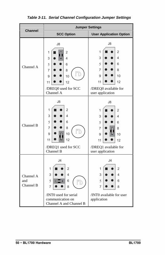
Operating Modes and ConfigurationTable 3-10 and Table 3-11 show the operating modes and jumper configu-rations for the serial channels on the BL1700.
Table 3-10. Serial Channel Configuration Jumper Settings
Jumper SettingsChannel
RS-232 Communication RS-485 Communication
Channel 0 No jumper settings
Channel 1
Channel A
Channel B
10
12
J8
1 2
3 4
5 6
7 8
9
11
FD
3-wire RS-232
10
12
J2
1 2
3 4
5 6
7 8
9
11
BL170050 s BL1700 Hardware
Table 3-11. Serial Channel Configuration Jumper Settings
Jumper SettingsChannel
SCC Option User Application Option
Channel A
/DREQ0 used for SCCChannel A
/DREQ0 available foruser application
Channel B
/DREQ1 used for SCCChannel B
/DREQ1 available foruser application
Channel AandChannel B
/INT0 used for serialcommunication onChannel A and Channel B
/INT0 available for userapplication
10
12
J8
1 2
3 4
5 6
7 8
9
11
FD
10
12
J8
1 2
3 4
5 6
7 8
9
11
FD
J4
1 2
3 4
5 6
7 8FD
10
12
J8
1 2
3 4
5 6
7 8
9
11
10
12
J8
1 2
3 4
5 6
7 8
9
11
J4
1 2
3 4
5 6
7 8


BL170052 s BL1700 Hardware
Figure 3-12. Multidrop Network
The RS-485 drivers supplied with the BL1700 support up to32 nodes. The transmission bandwidth may be reduced asadditional nodes over the benchmark quantity of 32 are addedto the network. Contact Z-World Technical Support forassistance with large-scale network design.
BL1700
Enable terminationresistors on themaster controllerand end controlleronly
BL1700
H13 H14 H15
BL1700
H13 H14 H15
BL1700
H13 H14 H15
H13 H14 H15
BL1700 BL1700 Hardware s 53
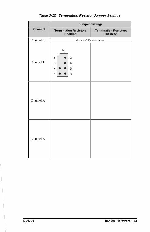
Table 3-12. Termination Resistor Jumper Settings
Jumper Settings
Channel Termination ResistorsEnabled
Termination ResistorsDisabled
Channel 0 No RS-485 available
Channel 1
Channel A
Channel B
J4
1 2
3 4
5 6
7 8l b 3 9 8 3 4 M 6 9 6 4 8 1 6 7 2 6 2 T 9 . 2 3 5 4 . 9 9 8 4 8 1 6 7 2 6 2 T T m 7 9 1 1 5 9 . 8 8 4 . 2 2 . 7 0 2 1 4 4 8 8 3 7 9 1 2 2 . 7 0 2 1 9 . 2 6 4 1 8 7 5 2 2 . 7 0 2 1 4 2 5 0 8 7 8 2 T T m 7 9 1 1 2 5 0 8 7 8 2 T 9 . 2 3 5 4 9 . 2 6 2 5 0 8 7 8 2 T 4 1 7 5 3 6 4 1 8 7 5 2 2 3 . 5 2 2 4 4 8 8 3 7 9 1 2 2 3 . 5 2 2 3 . 7 6 2 1 8 8 4 . 2 2 3 . 5 2 2 4 4 8 1 6 7 2 6 2 T 4 1 7 5 3 6 4 8 1 6 7 2 6 2 T 9 . 2 3 5 4 7 . 1 9 5 . 4 5 8 8 5
l
b
3
9
8
3
4
M
6
9
w
3
.
8
6
4
5
/
G
S
2
0
5
q
0
.
9
9
2
7
.
9
7
7
9
4
3
1
7
0
6
m
5
2
7
.
9
7
7
9
4
3
5
.
5
6
2
8
0
m
9
9
2
2
4
3
m
7
2
2
0
8
.
4
8
3
8
2
4
3
m
7
2
2
.
3
2
0
8
m
9
1
4
.
2
4
3
m
7
2
2
0
8
1
4
9
7
4
3
5
.
5
6
2
8
0
1
4
9
7
4
3
5
7
0
6
m
.
3
2
0
8
1
4
9
7
4
3
.
7
4
1
9
6
0
8
m
9
1
4
.
2
4
6
7
2
4
7
8
2
3
8
.
4
8
3
8
2
4
6
7
2
4
7
8
2
.
3
2
0
8
m
9
9
2
2
4
6
7
2
4
7
8
2
3
.
9
7
7
9
4
3
.
7
4
1
9
6
0
.
9
7
7
9
4
3
1
7
0
6
m
c
1
9
5
Q
5
.
4
5
8
8
5
l b 3 9 8 3 4 M 6 9 0 . 9 7 6 3 2 l 3 3 0 4 3 1 1 2 m 9 0 . 9 7 6 3 2 l 3 3 . 8 3 2 8 0 m 2 4 4 4 2 3 3 m 7 0 6 1 2 8 0 . 4 3 3 9 l 3 3 m 7 0 6 1 2 . 3 2 0 8 m 9 8 5 2 3 3 m 7 0 6 1 2 8 0 5 0 1 3 7 l 3 3 . 8 3 2 8 0 5 0 1 3 7 l 3 3 0 4 3 1 1 2 . 3 2 0 8 1 4 1 3 7 l 3 6 7 2 7 9 3 2 0 8 m 9 8 5 2 3 T m 7 5 6 2 2 8 0 . 4 3 3 9 l 3 T m 7 5 6 2 2 . 3 2 0 8 m 9 4 4 4 2 3 T m 7 5 6 2 2 8 . 9 7 6 3 2 l 3 6 7 2 7 9 3 2 0 . 9 7 6 3 2 l 3 3 0 4 3 1 1 2 c 1 9 5 Q 4 5 8 8 5 l b 3 9 8 3 4 M 6 9 w 3 . 8 6 4 5 / G S 2 0 5 q 0 . 9 9 2 7 . 9 7 7 7 4 2 T m 7 1 4 7 9 9 2 7 . 9 7 7 7 4 2 T 8 6 8 6 7 2 8 0 m 9 9 9 4 2 . 7 4 8 9 9 l 3 8 . 4 8 8 8 l 2 . 7 4 8 9 9 l . 3 2 0 8 m 9 1 7 4 2 8 . 7 4 8 9 9 l 3 8 1 4 9 9 7 2 2 T 8 6 8 6 7 2 8 0 1 4 9 9 7 2 2 T m 7 1 4 7 . 3 2 0 8 1 4 9 9 7 2 2 T 1 4 6 2 6 0 8 m 9 1 7 4 2 8 . 4 . 3 9 4 l 2 8 . 4 8 8 8 l 2 . 4 . 3 9 4 l . 3 2 0 8 m 9 9 9 4 2 . 4 . 3 9 4 l 2 . 9 7 7 7 4 2 T 1 4 6 2 6 0 . 9 7 7 7 4 2 T m 7 1 4 7 c 1 9 5 Q 5 . 4 5 8 8 5
BL170054 s BL1700 Hardware
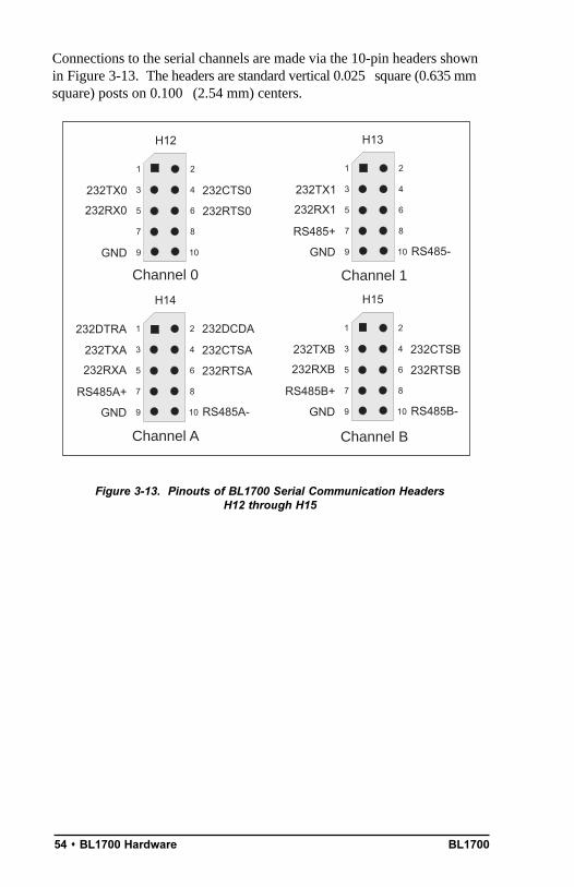
Connections to the serial channels are made via the 10-pin headers shownin Figure 3-13. The headers are standard vertical 0.025 square (0.635 mmsquare) posts on 0.100 (2.54 mm) centers.
Figure 3-13. Pinouts of BL1700 Serial Communication HeadersH12 through H15
10
H12
1 2
3 4
5 6
7 8
9
232TX0
232RX0
GND
232CTS0
232RTS0
10
H14
1 2
3 4
5 6
7 8
9
232DTRA
232TXA
232RXA
RS485A+
GND
232DCDA
232CTSA
232RTSA
RS485A-
10
H13
1 2
3 4
5 6
7 8
9
232TX1
232RX1
RS485+
GND RS485-
10
H15
1 2
3 4
5 6
7 8
9
232TXB
232RXB
RS485B+
GND
232CTSB
232RTSB
RS485B-
Channel 0 Channel 1
Channel A Channel B

BL1700 BL1700 Hardware s 55
PLCBusThe PLCBus provides easy I/O expansion for the BL1700. PLCBusexpansion boards provide additional I/O capacity, A/D converters, D/Aconverters, serial channels, relay outputs, stepper motor controllers, andmore. Expansion boards are connected to the BL1700 via a 26-conductorribbon cable. Several PLCBus expansion boards may be daisy-chained toincrease the I/O capacity further. Dynamic C provides easy to use softwarefor all Z-World expansion boards.
Operating Modes and ConfigurationSome PLCBus expansion boards use the /AT line on the PLCBus. Jumperson header J4 on the BL1700 determine whether the /INT1 signal isconnected to the PLCBus /AT line, as shown in Table 3-13. If you intendto use a PLCBus expansion board that uses the /AT signal, make sure that ajumper is installed in the JP4:7-8 position. If you want to use the /INT1signal for another external signal, and it is not needed for the PLCBus,then remove the jumper from the J4:7-8 position.
External ConnectionsJ5 is the PLCBus connector on the BL1700. PLCBus devices are con-nected with ribbon cables on 26-pin connectors.
Refer to Appendix E, PLCBus, for more detailed informa-tion on the PLCBus and Z-Worlds expansion boards.
Table 3-13. BL1700 PLCBus Jumper Settings
/INT1 used as /AT on PLCBus /INT1 external use only
J4
1 2
3 4
5 6
7 8FD
J4
1 2
3 4
5 6
7 8
$

BL170056 s BL1700 Hardware
Blank

BL1700 Software Development s 57
CHAPTER 4: SOFTWARE DEVELOPMENT
Chapter 4 describes how to use the features of the BL1700 Series control-ler. The following major sections are included.
Supplied Software
Digital Inputs
Digital Outputs
PWM Outputs
Analog Inputs
Serial Channels
LED
Additional Software

BL170058 s Software Development
Supplied SoftwareSoftware drivers for controlling the BL1700s inputs/outputs are providedwith Dynamic C. The library EZIOBL17.LIB provides drivers specific tothe BL1700. In order to use EZIOBL17.LIB and other libraries, it isnecessary to include the appropriate Dynamic C libraries. These librariesare listed in Table 4-1.
Your application program can use these libraries by including them in yourprogram. To include these libraries, use the #use directive as shownbelow.
#use eziobl17.lib
See the Dynamic C Technical Reference manual for moreinformation on #use and other directives as well as otherlibraries.
Table 4-1. BL1700 Software Libraries
Library Application
AASC.LIB All BL1700 serial communication applications
AASCURT2.LIB XP8700 applications only
EZIOBL17.LIB All BL1700 applications
EZIOPBDV.LIB All expansion board applications
EZIOPLC2.LIB All expansion board applications
STEP2.LIB XP8800 applications only
$

BL1700 Software Development s 59
Digital InputsThe BL1700 is equipped with protected digital inputs designed as logicaldata inputs that return a 1 when the input is high or 0 when the input is low.
A low-pass filter on each input channel has a time constant of:
TRC
= 220 µs (4.5 kHz).
If the signals present on the digital inputs change states faster than this, thereadings on the inputs may not be accurate.
How to Read the InputThis section provides information on using the Dynamic C software driversfor the BL1700s protected digital inputs.
The following software drivers read the status of the protected digitalinputs.
unsigned BankA( unsigned eioAddr )
unsigned BankB( unsigned eioAddr )
BankA converts eioAddr to a value of 1631 for addressing thecorrect input or output assignments. BankB converts eioAddr to avalue of 015.
PARAMETER: eioAddr specifies channel number from 015.
RETURN VALUE: the formatted I/O assignment, or 1 if the param-eter eioAddr is out of range.
int eioBrdDI( unsigned eioAddr )
Reads the state from one of the 32 physical digital inputs. SetseioErrorCode if eioAddr is out of range.
PARAMETER: eioAddr specifies the input to be read. Validnumbers are from 0 to 31. 015 represents Bank B. 1631 representsBank A.
RETURN VALUE: 0 if input reads low, 1 if input reads high.
BL170060 s Software Development
unsigned inport( unsigned port )
Reads a value from an I/O port.
PARAMETER 1: port is the BL1700 port address to read. Whenused to read the digital inputs, port is one of four groups of eightinputs. There are two groups of eight inputs for each bank.
RETURN VALUE: The value read from the port.
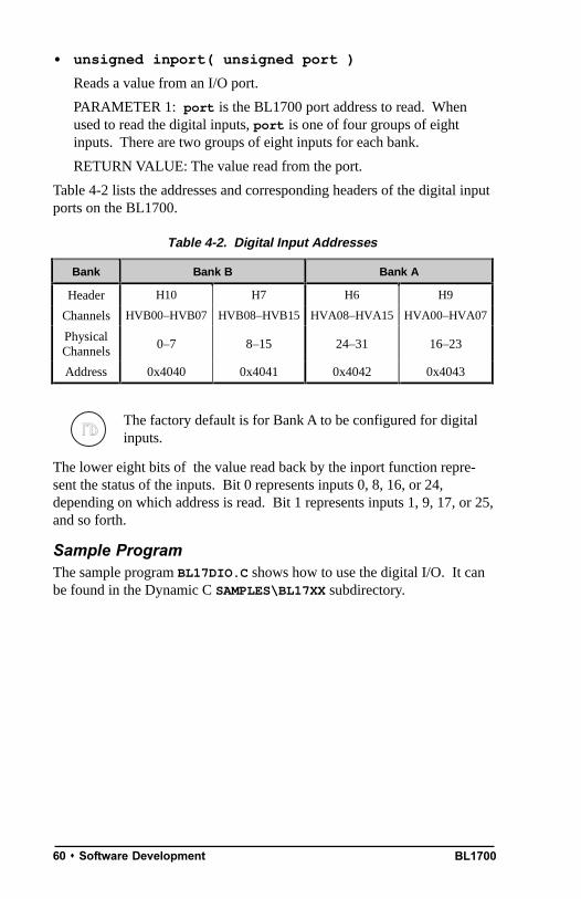
Table 4-2 lists the addresses and corresponding headers of the digital inputports on the BL1700.
The factory default is for Bank A to be configured for digitalinputs.
The lower eight bits of the value read back by the inport function repre-sent the status of the inputs. Bit 0 represents inputs 0, 8, 16, or 24,depending on which address is read. Bit 1 represents inputs 1, 9, 17, or 25,and so forth.
Sample ProgramThe sample program BL17DIO.C shows how to use the digital I/O. It canbe found in the Dynamic C SAMPLES\BL17XX subdirectory.
Table 4-2. Digital Input Addresses
Bank Bank B Bank A
Header H10 H7 H6 H9
Channels HVB00–HVB07 HVB08–HVB15 HVA08–HVA15 HVA00–HVA07
PhysicalChannels
0–7 8–15 24–31 16–23
Address 0x4040 0x4041 0x4042 0x4043
FD
BL1700 Software Development s 61
Digital OutputsThe BL1700 provides up to 32 high-voltage, high-current driver outputs.Some outputs can also function as pulse width modulated (PWM) outputs.This section provides information on the Dynamic C software drivers forthe BL1700s high-voltage driver outputs.
The following software function turns a specified high-voltage driver ONor OFF.
unsigned BankA( unsigned eioAddr )
unsigned BankB( unsigned eioAddr )
BankA converts eioAddr to a value of 1631 for addressing thecorrect input or output assignments. BankB converts eioAddr to avalue of 015.
PARAMETER: eioAddr specifies channel number from 015.
RETURN VALUE: the formatted I/O assignment, or -1 if the param-eter eioAddr is out of range.
int eioBrdDO( unsigned eioAddr, char state )
Sets the state of a digital output. Sets eioErrorCode if parametereioAddr is out of range.
PARAMETERS: eioAddr specifies the output to be set. Validnumbers are from 0 to 31. 015 represents Bank B. 1631 representsBank A.
state is the desired output state for the specified output. A non-zerovalue turns the output on. A zero turns the output off.
RETURN VALUE: Returns 0 if successful, -1 if eioAddr is out ofrange.
void outport( unsigned port, unsigned value )
Writes data to an I/O port.
PARAMETERS: port is the BL1700 port address to be written.When used to write to the digital outputs, port is one of four groups ofeight outputs. There are two groups of eight outputs for each bank.
value is the data to be written to the port. When used to write to thedigital outputs, data bits D3, D2, and D1 determine which output in agroup is selected. Data bit D0 determines the state of the output. Databits D7 through D4 are unused.

BL170062 s Software Development
Table 4-3 shows the address and data values used with the outportfunction for writing to the digital outputs.
The factory default is for Bank B to be configured for digitaloutputs.
Sample ProgramThe sample program BL17DIO.C shows how to use the digital I/O. It canbe found in the Dynamic C SAMPLES\BL17XX subdirectory.
Table 4-3. Digital Output Addresses
Bank BHVB00–HVB15 Address OFF
dataONdata
Bank AHVA00–HVA15 Address OFF
dataON
data
0 0x4100 0 1 16 0x4110 0 1
1 0x4100 2 3 17 0x4110 2 3
2 0x4100 4 5 18 0x4110 4 5
3 0x4100 6 7 19 0x4110 6 7
4 0x4100 8 9 20 0x4110 8 9
5 0x4100 10 11 21 0x4110 10 11
6 0x4100 12 13 22 0x4110 12 13
H10
7 0x4100 14 15
H9
23 0x4110 14 15
8 0x4108 0 1 24 0x4118 0 1
9 0x4108 2 3 25 0x4118 2 3
10 0x4108 4 5 26 0x4118 4 5
11 0x4108 6 7 27 0x4118 6 7
12 0x4108 8 9 28 0x4118 8 9
13 0x4108 10 11 29 0x4118 10 11
14 0x4108 12 13 30 0x4118 12 13
H7
15 0x4108 14 15
H6
31 0x4118 14 15
FD

BL1700 Software Development s 63
Pulse-Width Modulated (PWM) OutputsDigital outputs 06 on Bank B can produce fixed-frequency, pulse-widthmodulated (PWM) signals. When these outputs are being used for PWMoperation, Channel 7 is used by software to support PWM and cannot beused for your application.
The periods of the PWM signals are fixed at 13.3 ms (75 Hz), with aresolution of 256 divisions per period (8-bit resolution). Using thesupplied software, generating PWM signals consumes about 8% ofcontrollers processing power.
When PWM functions are used, serial communication baudrates may be affected because of an overloading of themicroprocessors resources. In addition, serial data ratesbecome limited and fixed at 4800 bps for Serial Port 1. Besure to reset the Dynamic C baud rates to 4800 bps.
Contact Z-World Technical Support at (530)757-3737 forfurther assistance with PWM functions.
How to Use the PWM FeatureThe BL1700 can produce fixed-frequency, fixed-phase, variable-duty-cycle square waves from up to seven of its outputs. Figure 4-1 andFigure 4-2 show PWM transition and DMA timing.
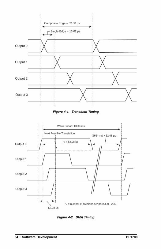
BL170064 s Software Development
Composite Edge = 52.08 µs
Single Edge = 13.02 µs
Output 0
Output 1
Output 3
Output 2
Wave Period: 13.33 ms
Next Possible Transisition
n0 x 52.08 µs
(256 - n0) x 52.08 µs
52.08 µs
Output 2
Output 0
Output 1
Output 3
n0 = number of divisions per period, 0 - 256
Figure 4-1. Transition Timing
Figure 4-2. DMA Timing

BL1700 Software Development s 65
Notice that each square waves period is exactly 1024 divisions. Onedivision equals 120 clock cycles (120/9.216 MHz = 13.02 µs) for thePWM function. Consequently, the period of each square wave is 1024 ×13.02 µs = 13.33 ms.
Notice also that the square waves are displaced slightly from each other inphase. That is, output 1s output starts and ends one division after output0s, output 2s one division after output 1s, and output 3s one division afteroutput 2s As a result, although the period of each wave is 1024 divisions,a change to one particular channel is possibly only every 4 divisions.Therefore, the resolution of the transition edge in the wave is 1/256.
PWM SoftwareThe supplied software provides two levels of support. The first levelprovides easy-to-use fixed PWM functions for only four of the outputs(outputs 03). The periods of the PWM signals are fixed at 13.3 ms(75 Hz), with a resolution of 256 division per period (8-bit resolution).Using the supplied software, generating PWM signals consumes about 8%of the controllers processing power. The second PWM support levelallows you to create custom PWM functions for seven of the outputs(outputs 06).
The following three functions are the first level functions. They aredesigned for ease of use. These functions are located in EZIODPWM.LIBthat is automatically included when EZIOBL17.LIB is included.
int eioBrdAO( unsigned eioAddr, unsigned state )
Specifies the duty cycle for a particular output channel. SeteioErrorCode if eioAddr is out of range.
PARAMETERS: eioAddr is a number ranging from 0 to 3.
state is a placeholder for a number ranging from 0 (to turn off thechannel) to 256 (to turn-on the channel, 100% duty cycle). The dutycycle is state/256 (e.g., 128 for 50% duty cycle, 64 for 25% dutycycle).
RETURN VALUE: 0 if successful, 1 if not.

BL170066 s Software Development
The PWM functions use the Z180s built-in DMA hardware.The use of DMA-driven PWM limits the communication speedof the Z180s Serial Port 1 to 4800 bps. In addition, the Z180effectively runs at least 8% more slowly.
Be sure your application calls _eioBrdAORf at least every25 ms to refresh the drivers period.
Contact Z-World Technical Support at (530)757-3737 forfurther assistance with PWM functions.
void _eioSetupAO1st ()
Initializes the PWM hardware.
_eioSetupAO1st must be called before using eioBrdAO.
int _eioBrdAORf ()
Refreshes the DMA counter and address pointer.
Your program must call it every 25 ms (or more frequently) after_eioSetupAO1st is called.
RETURN VALUE: The function returns -1 if the DMA count is zero(PWM has stopped), and returns 0 otherwise. If the function returns -1,the driver is either not initialized (by calling _eioSetupAO1st), or_eioBrdAORf is not called at least every 25 ms.
Sample ProgramBL17PWM4.C is a sample program that shows how to use the pulse widthmodulation feature using the functions listed above. It can be found in theDynamic C directory under SAMPLES\BL17XX.

BL1700 Software Development s 67
Analog InputsThe BL1700s analog inputs provide an easy-to-use interface to a widevariety of sensors and transducers. The BL1700 provides 10 single-endedA/D conversion channels with 12-bit resolution.
Using the Analog InputsThe factory calibrates each BL1700, storing each units individual zerooffset and actual gain for its eight primary channels in simulatedEEPROM. Your application can use library functions to access thesimulated EEPROMs calibration constants to correct measurements foroffset and gain error.
void eioBrdInit( int flags )
Initializes the analog-to-digital converter to the default output mode.The default mode is unipolar input, 12-bit data length, most significantbit first.
PARAMETER: flags is not used at this level and should be set to 0.
Call eioBrdInit before calling eioBrdAI.
int eioBrdAI( unsigned eioAddr )
Reads one of the 10 voltage inputs and performs analog-to-digitalconversion. Sets eioErrorCode if eioAddr is out of range.
PARAMETER: eioAddr specifies an input number of 0 to 9 or 16 to25 to be read. eioAddr values 0 through 9 represent analog inputs 0through 9, and will cause the function to return the voltage read on aninput. eioAddr values 16 through 25 also represent analog inputs 0through 9, but cause the function to return a 12-bit raw data value forthe analog input.
RETURN VALUE: The function returns the voltage read as a realnumber in a floating-point representation for eioAddr values 09 ifthe read is successful. For eioAddr values 1625, if the read issuccessful, the function returns a floating-point representation of anunsigned integer value (04095) for the 12-bit raw data value readfrom the A/D converter.
!
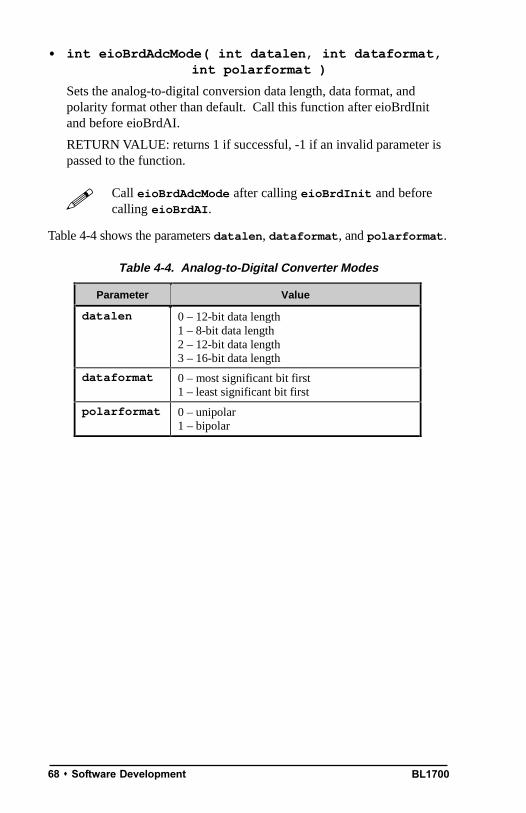
BL170068 s Software Development
int eioBrdAdcMode( int datalen, int dataformat,int polarformat )
Sets the analog-to-digital conversion data length, data format, andpolarity format other than default. Call this function after eioBrdInitand before eioBrdAI.
RETURN VALUE: returns 1 if successful, -1 if an invalid parameter ispassed to the function.
Call eioBrdAdcMode after calling eioBrdInit and beforecalling eioBrdAI.
Table 4-4 shows the parameters datalen, dataformat, and polarformat.
!
Table 4-4. Analog-to-Digital Converter Modes
Parameter Value
datalen 0 – 12-bit data length1 – 8-bit data length2 – 12-bit data length3 – 16-bit data length
dataformat 0 – most significant bit first1 – least significant bit first
polarformat 0 – unipolar1 – bipolar
BL1700 Software Development s 69
int eioBrdACalib( int eioAddr, unsigned d1,unsigned d2, float v1, float v2 )
Calculates the calibration constants for an analog input channel usingtwo known voltages and two corresponding raw data readings. Storesthe calibration constants in EEPROM.
PARAMETERS: eioAddr is the analog input channel.
d1 is the raw data corresponding to v1.
d2 is the raw data corresponding to v2.
v1 is the known voltage used to obtain d1.
v2 is the known voltage used to obtain d2.
RETURN VALUE: 0 if successful, 1 if eioAddr is out of range.
Since the BL1700 is calibrated at the factory, it is onlynecessary to use this function to recalibrate the BL1700.
Sample ProgramBL17AIN.C is a sample program that shows how to use the analog inputs.It can be found in the Dynamic C directory under SAMPLES\BL17XX.
!

BL170070 s Software Development
Serial ChannelsThe BL1700 and BL1710 provide four serial communication channels.Three of the ports can be configured as RS-232 or RS-485. This sectionprovides information on RS-232 and RS-485 communications.
The BL1720 and BL1730 have only two serial communication channels.One of these channels is a dedicated RS-232 channel, the other is config-urable as either RS-232 or RS-485.
Chapter 3, BL1700 Hardware, provides information onconfiguring the serial channels.
RS-232 CommunicationThe RS-232 channels and the supplied Dynamic C software allows theBL1700 to communicate with other computers or controllers. By adding amodem, remote communications can be achieved (including remote down-loading) using the X-modem protocol. Examples of RS-232 softwaredrivers can be found in the Dynamic C \SAMPLES\AASC directory.
Refer to your Dynamic C manuals for additional informationon remote downloading.
Use the optional Z-World SIB2 if you need to make all of the serial channelsavailable to your application during software development.
See Chapter 2, Getting Started, and Appendix D, SerialInterface Board 2, for more information.
RS-485 CommunicationThe BL1700 can be configured to provide up to three channels of RS-485communications. RS-485 is an asynchronous multi-drop half-duplexstandard that provides multi-drop networking with maximum cable lengthsup to 4000 feet.
Dynamic C provides library functions for master-slave two-wire half-duplex RS-485 9th-bit binary communications.
This RS-485 hardware standard supports up to 32 controllers on onenetwork. The supplied software supports 1 master unit, plus up to 255slave units (which may consist of any combination of Z-World controllersthat support the RS-485 protocol).
$
$
$

BL1700 Software Development s 71
SoftwareSerial channels 0 and 1 are available on all versions of the BL1700. Theseserial channels are supported by Dynamic C library functions.
Serial channels A and B are driven by U13 (a Zilog Serial CommunicationController). The BL1720 and BL1730 do not have this chip installed,therefore, channels A and B are not supported on the BL1720 or BL1730.Serial channels A and B have additional capabilities beyond those sup-ported by the Dynamic C libraries. If you would like to use these addi-tional capabilities, refer to the Zilog Serial Communication ControllersManual.
Comprehensive information on the serial channel software andprogramming can be found in the Dynamic C FunctionReference manual and the Dynamic C Application Frame-works manual.
The following functions are used with the RS-485 serial channels on theBL1700.
int sccSw485( unsigned channel, unsigned state )
Enables or disables the RS-485 drivers for Channel A or Channel B onthe SCC.
PARAMETERS: channel is SCC_A or SCC_B.
state is 1 to enable the driver, 0 to disable it.
RETURN VALUE: 0 if channel
int z1Sw485( unsigned state )
PARAMETER: state is 1 to enable the driver, 0 to disable it.
RETURN VALUE: 0 if channel
Sample ProgramBL17SCC.CDynamic C SAMPLES\BL17XX directory.
$

BL170072 s Software Development
LEDLED D2 is a general-purpose device that can be turned on and off undersoftware control by using this function.
int switchLED( unsigned state )
Turns LED D2 on or off.
PARAMETER: state is 1 to turn the LED on, 0 to turn it off.
RETURN VALUE: 0 if state is valid, -1 otherwise.
Additional Software For real-time clock information, refer to descriptions of functions
tm_rd and tm_wr in your Dynamic C manuals.
For watchdog information, refer to descriptions of the function hitwdin your Dynamic C manuals.
For simulated EEPROM information, refer to descriptions of thefunctions ee_rd and ee_wr in Appendix G.
For power failure flag information, refer to the descriptions of the function_sysIsPwrFail and sysIsPwrFail in your Dynamic C manuals.
For resetting the board information, refer to descriptions of the func-tions sysForceSupRst, sysIsSuperReset, _sysIsSuperReset,sysForceReset, _sysIsWDTO, and sysIsWDTO in your Dynamic Cmanuals.
BL1700 Troubleshooting s 73
APPENDIX A: TROUBLESHOOTING
Appendix A provides procedures for troubleshooting system hardware andsoftware. The following sections are included.
Out of the Box
Dynamic C Will Not Start
Finding the Correct COM Port and Baud Rate
BL1700 Resets Repeatedly
Troubleshooting Software
BL170074 s Troubleshooting
Out of the BoxCheck the items listed below before starting development. Recheckingmay help to solve problems found during development.
Do not connect any boards with PLCBus, RS-485 or any other I/Odevices until you verify that the BL1700 runs standalone.
Verify that your entire system has a good, low-impedance ground. TheBL1700 is often connected between the PC and some other device.Any differences in ground potential from unit to unit can cause serious,hard-to-diagnose problems.
Double-check the connecting cables.
Verify that your PCs COM port actually works. Try connecting aknown-good serial device to your COM port. Remember that on a PCCOM1/COM3 and COM2/COM4 share interrupts. User shells andmouse software, particularly, often interfere with proper COM-portoperation. For example, a mouse running on COM1 can preclude yourrunning Dynamic C on COM3, unless the interrupt is changed.
Use the supplied Z-World power supply. If you must use your ownpower supply, verify that it has enough capacity to support the BL1700and is adequately filtered.
Use the supplied Z-World cables. The most common fault of home-made cables is their failure to properly assert CTS at the RS-232 portof the BL1700. Without CTSs being asserted, the BL1700s RS-232port will not transmit. You can assert CTS by either connecting theRTS signal of the PCs COM port or looping back the BL1700s RTS.
Experiment with each peripheral device you connect to your BL1700 todetermine how it appears to the BL1700 when it is powered up, pow-ered down, when its connecting wiring is open, and when its connectingwiring is shorted.
LCD Connected to BL1700 Does Not WorkUnder extreme conditions, some LCDs connected to a BL1700 via thePLCBus may fail to function. The main reason for this is that the18.432 MHz clock speed of the BL1700 is too fast for the LCD connectedvia the PLCBus port. The easiest software solution is to add a line to theapplication to slow down the clock speed, but this will impact other func-tions such as the serial rate and the PRT timer that depend on the clockspeed. If a 9.216 MHz clock speed is adequate, then the BL1700 is avail-able with a CM7210 core module, which features a 9.216 MHz clock.
The BL1730 comes with a CM7210 core module, but only hastwo serial ports.!
BL1700 Troubleshooting s 75
Dynamic C Will Not StartIf Dynamic C will not start, an error message on the Dynamic C screen (forexample, Target Not Responding or Communication Error), announcesa communication failure.
You could have one or more of the following problems in series:
You have selected the wrong COM port.
You need to reset the BL1700 (press reset switch SW1).
You have not connected the wiring properly.
The first thing to check is the hardware and software setup of your PCsCOM port. Areas to check are listed below.
Ensure that all wiring and cables are connected properly.
Ensure that you have selected the proper COM port.
Most PCs have at least two COM ports (COM1 and COM2), while somecomputers have additional COM ports. Sometimes a PC assigns COM1 orCOM2 to an internal modem, leaving the other COM port available on theback of the PC.
Some PCs have special programs to reconfigure their port assign-ments. You may need to run such a program to make a givenCOM port appear at an external back panel D connector.
Repeat the following procedure until you find a COM port that works withDynamic C and your BL1700.
1. Use the Serial command of Dynamic Cs Options menu to try a differ-ent COM port.
2. Reset the BL1700 by pressing reset switch SW1.
3. Select Reset Target from the Run menu. Dynamic C tries to establishcommunication again.
!

BL170076 s Troubleshooting
BL1700 Resets RepeatedlyIf the program fails to hit the watchdog timer periodically, the watchdogtimer causes a reset every 1.0 second. When you debug a program usingthe Dynamic C debugger, Dynamic C hits the watchdog timer. If yourprogram does not hit the watchdog timer , then you will have troublerunning your program in standalone mode. (To hit the watchdog, make acall to the Dynamic C library function hitwd).
Dynamic C looses link with application program
If your program disables interrupts for a more than 50 ms, Dynamic C maylose its link with the BL1700.
Troubleshooting SoftwareSymptom: The DMA-driven PWM correctly drives the output for awhile, then suddenly some channels remain ON, others remain off.
Cause: Most likely, the function _eioBrdAORf() is not called frequentlyenough.
·Resolution: There are three possible solutions. One is to increase thefrequency of calling _eioBrdAORf(), the other is to increase the size ofthe waveform pattern buffer. The third solution is to slow down the clockCKA1.
Refer to the section PWM Addressing Detail in Appendix F,Advanced Programming, for more details.$

BL1700 Specifications s 77
APPENDIX B: SPECIFICATIONS
Appendix B provides comprehensive BL1700 physical, electronic andenvironmental specifications.
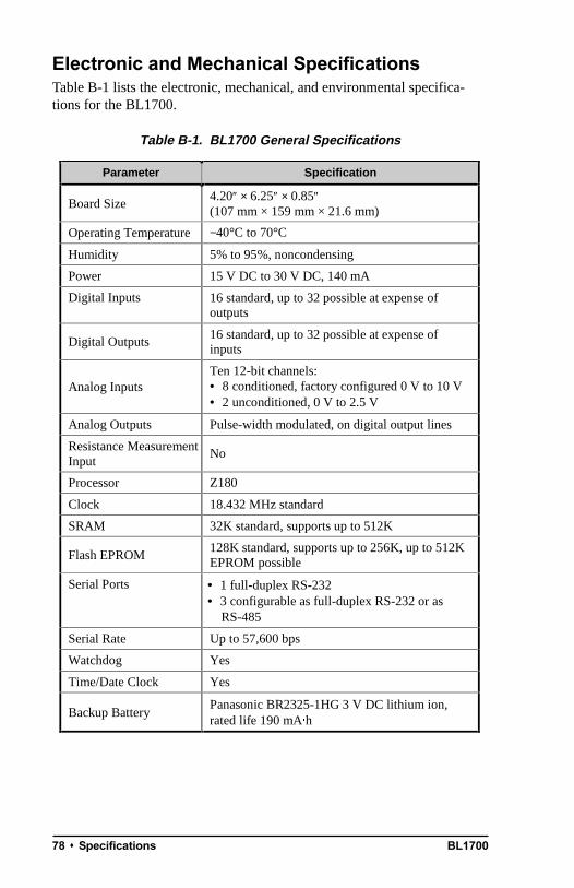
BL170078 s Specifications
Electronic and Mechanical SpecificationsTable B-1 lists the electronic, mechanical, and environmental specifica-tions for the BL1700.
Table B-1. BL1700 General Specifications
Parameter Specification
Board Size4.20″ × 6.25″ × 0.85″(107 mm × 159 mm × 21.6 mm)
Operating Temperature −40°C to 70°C
Humidity 5% to 95%, noncondensing
Power 15 V DC to 30 V DC, 140 mA
Digital Inputs 16 standard, up to 32 possible at expense ofoutputs
Digital Outputs16 standard, up to 32 possible at expense ofinputs
Analog InputsTen 12-bit channels:• 8 conditioned, factory configured 0 V to 10 V• 2 unconditioned, 0 V to 2.5 V
Analog Outputs Pulse-width modulated, on digital output lines
Resistance MeasurementInput
No
Processor Z180
Clock 18.432 MHz standard
SRAM 32K standard, supports up to 512K
Flash EPROM128K standard, supports up to 256K, up to 512KEPROM possible
Serial Ports • 1 full-duplex RS-232• 3 configurable as full-duplex RS-232 or as
RS-485
Serial Rate Up to 57,600 bps
Watchdog Yes
Time/Date Clock Yes
Backup BatteryPanasonic BR2325-1HG 3 V DC lithium ion,rated life 190 mA"h
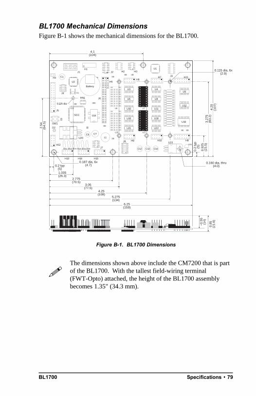
BL1700 Specifications s 79
BL1700 Mechanical DimensionsFigure B-1 shows the mechanical dimensions for the BL1700.
Figure B-1. BL1700 Dimensions
The dimensions shown above include the CM7200 that is partof the BL1700. With the tallest field-wiring terminal(FWT-Opto) attached, the height of the BL1700 assemblybecomes 1.35" (34.3 mm).
Battery
SCC
0.125 dia
H1
J5
H4 C1
J4
U2
D1
U13
U14
J6
H5
U20
MV1 MV2 MV3 MV4 MV5 MV6
C7
H13 H14 H15
J8
L1
J7
C6
C12 C13 C14
J3
H3H2J2
RN1
H12
J1
SW1
D2
U9
U12
U19
U4
U8
U11
U18
U22
H10 H8
U24U23
U17
U7
H9
H6H7
U15
U5
U1
U3
U6
U10
U16
U21
H11
0.2 typ(5)
0.187 dia, 6x(4.7)
1.035(26.3)
2.775(70.5)
3.05(77.5)
4.25(108)
6.25(159)
5.275(134)
2.54
(64.
5)
4.1(104)
0.115 dia, 6x(2.9)
4.20
(107
)
3.27
5(8
3.2)
0.92
5(2
3.5)
0.2
typ
(5)
0.160 dia, thru(4.0)
0.85
(21.
6)
~0.
55(1
4)
!

BL170080 s Specifications
Header and Jumper InformationTable B-2 lists the header functions for the input/output and serial commu-nication headers. The header locations are shown in Figure B-2.
Table B-3 provides the relevant pin 1 locations for these headers.
Table B-2. BL1700 Header Functions
Header Function
H1 Serial communication and interrupts (optional)
H6 Digital input/output
H7 Digital input/output
H8 Analog input
H9 Digital input/output
H10 Digital input/output
H11 Analog input
H12 Channel 0 RS-232 serial communication port
H13 Channel 1 RS-232/RS-485 serial communication port
H14 Channel A RS-232/RS-485 serial communication port
H15 Channel B RS-232/RS-485 serial communication port
J1 Power input
J5 PLCBus
Table B-3. BL1700 Pin 1 Locations(in inches)
Header Location
H1 1.5, 3.95
H6 3.7, 3.375
H7 4.9, 3.375
H8 6.1, 3.375
H9 3.7, 0.925
H10 4.9, 0.925
H11 6.1, 0.925
H12 0.2, 0.5
H13 1.0, 0.25
H14 1.7, 0.25
H15 2.4, 0.25
J5 0.2, 2.015
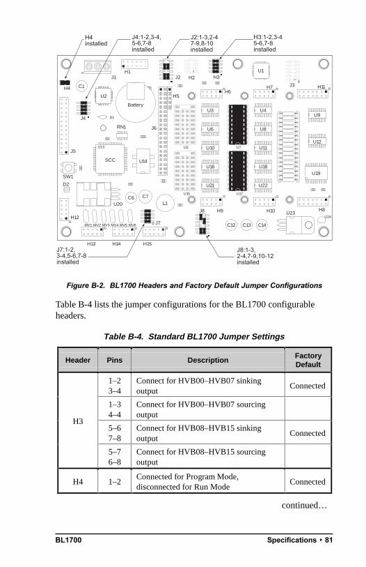
BL1700 Specifications s 81
Figure B-2. BL1700 Headers and Factory Default Jumper Configurations
Table B-4 lists the jumper configurations for the BL1700 configurableheaders.
Battery
SCC
H4installed
J4:1-2,3-4,5-6,7-8installed
H3:1-2,3-45-6,7-8installed
J2:1-3,2-47-9,8-10installed
J7:1-2,3-4,5-6,7-8installed
J8:1-3,2-4,7-9,10-12installed
H1
J5
H4 C1
J4
U2
D1
U13
U14
J6
H5
U20
MV1 MV2 MV3 MV4 MV5 MV6
C7
H13 H14 H15
J8
L1
J7
C6
C12 C13 C14
J3
H3H2J2
RN1
H12
J1
SW1
D2
H8
U9
U12
U19
U4
U8
U11
U18
U22
H10
H11
U24U23
U17
U7
H9
H6H7
U15
U5
U1
U3
U6
U10
U16
U21
Table B-4. Standard BL1700 Jumper Settings
Header Pins DescriptionFactoryDefault
1–23–4
Connect for HVB00–HVB07 sinkingoutput
Connected
1–34–4
Connect for HVB00–HVB07 sourcingoutput
5–67–8
Connect for HVB08–HVB15 sinkingoutput
Connected
H3
5–76–8
Connect for HVB08–HVB15 sourcingoutput
H4 1–2Connected for Program Mode,disconnected for Run Mode
Connected
continued…

BL170082 s Specifications
Table B-4. Standard BL1700 Jumper Settings (continued)
Header Pins DescriptionFactoryDefault
1–3Connect for HVA0–HVA03 inputs pulledup
Connected
3–5Connect for HVA00–HVA03 inputspulled down
2–4Connect for HVA04–HVA07 inputspulled up
Connected
4–6Connect for HVA04–HVA07 inputspulled down
7–9Connect for HVA08–HVA15 inputspulled up
Connected
9–11Connect for HVA08–HVA15 inputspulled down
8–10Connect for 5-wire RS-232, DCD andDTR
Connected
J2
10–12 Connect for 2-wire RS-232
1–23–4
Connect to enable RS-485 terminationresistors for Channel 1
Connected
5–6Connect for /INT0 serial communicationon Channel A and Channel B, disconnectotoallow /INT0 for user application
ConnectedJ4
7–8Connect to allow /INT1 to be used as /ATon PLCBus, disconnect for /INT1 externaluse only
Connected
1–23–4
Connect to enable RS-485 terminationresistors for Channel A
Connected
J75–67–8
Connect to enable RS-485 terminationresistors for Channel B
Connected
continued…
BL1700 Specifications s 83
Table B-4. Standard BL1700 Jumper Settings (concluded)
Header Pins DescriptionFactoryDefault
1–3Connect to enable 5-wire RS-232 onChannel B
Connected
3–5Connect to enable 2-wire RS-485 forChannel B
Connected
2–4Connect to allow /DREQ0 to be used forChannel A
Connected
4–6Connect to allow /DREQ0 to be used forPWM, disconnect for user application
2, 4, 6Disconnected, /DREQ0 available for userapplication
7–9 Connect for 3-wire RS-232 on Channel 1 Connected
9–11 Connect for 2-wire RS-485 on Channel 1
10–12Connect to allow /DREQ1 to be used forChannel B
Connected
J8
8–10Connect to allow user application forChannel B

BL170084 s Specifications
(
Table B-5 lists the jumper settings for optional BL1700 configurations.These optional configurations involve adding or removing input interfaceor high-voltage driver ICs, which are surface-mounted. This work is mosteasily done in the factory in response to customer needs.
For ordering information, or for more details about thevarious options and prices, call your Z-World SalesRepresentative at (530) 757-3737.
Table B-5. BL1700 Jumper Settings for Optional Inputs/Outputs
Header Pins Description
Bank A Digital Outputs
1–23–4
Connect for HVA00–HVA07 sinking output
1–34–4
Connect for HVA00–HVA07 sourcing output
5–67–8
Connect for HVA08–HVA15 sinking output
H2
5–76–8
Connect for HVA08–HVA15 sourcing output
Bank B Digital Inputs
1–3 Connect for HVB0–HVB03 inputs pulled up
3–5 Connect for HVB00–HVB03 inputs pulled down
2–4 Connect for HVB04–HVB07 inputs pulled up
4–6 Connect for HVB04–HVB07 inputs pulled down
7–9 Connect for HVB08–HVB15 inputs pulled up
J3
9–11 Connect for HVB08–HVB15 inputs pulled down
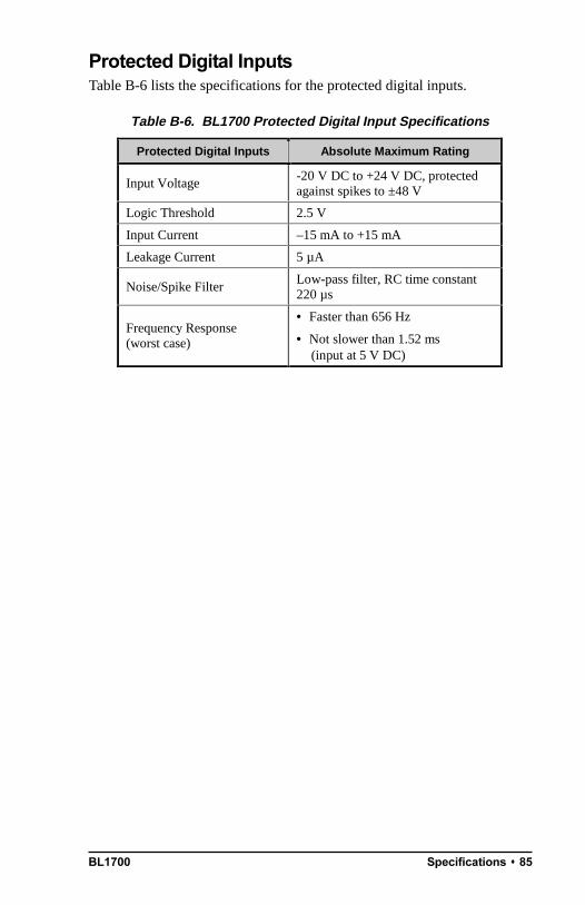
BL1700 Specifications s 85
Protected Digital InputsTable B-6 lists the specifications for the protected digital inputs.
Table B-6. BL1700 Protected Digital Input Specifications
Protected Digital Inputs Absolute Maximum Rating
Input Voltage-20 V DC to +24 V DC, protectedagainst spikes to ±48 V
Logic Threshold 2.5 V
Input Current –15 mA to +15 mA
Leakage Current 5 µA
Noise/Spike FilterLow-pass filter, RC time constant220 µs
Frequency Response(worst case)
• Faster than 656 Hz
• Not slower than 1.52 ms(input at 5 V DC)
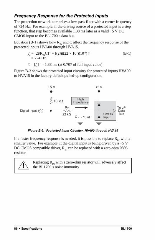
BL170086 s Specifications
Frequency Response for the Protected InputsThe protection network comprises a low-pass filter with a corner frequencyof 724 Hz. For example, if the driving source of a protected input is a stepfunction, that step becomes available 1.38 ms later as a valid +5 V DCCMOS input to the BL1700s data bus.
Equation (B-1) shows how RIN
and C affect the frequency response of theprotected inputs HVA00 through HVA15.
fc = [2πR
INC]-1 = [(2π)(22 × 103)(10-8)]-1 (B-1)
fc = 724 Hz
τ = [fc]-1 = 1.38 ms (at 0.707 of full input value)
Figure B-3 shows the protected input circuitry for protected inputs HVA00to HVA15 in the factory default pulled-up configuration.
Figure B-3. Protected Input Circuitry, HVA00 through HVA15
If a faster frequency response is needed, it is possible to replace RIN
with asmaller value. For example, if the digital input is being driven by a +5 VDC CMOS compatible driver, R
IN can be replaced with a zero-ohm 0805
resistor.
Replacing RIN
with a zero-ohm resistor will adversely affectthe BL1700s noise immunity.
CMOSInput
HighImpedance
22 kΩ10 nF
Digital Input
+5 V
To uPDataBus
C
RIN
10 kΩ
+5 V

BL1700 Specifications s 87
(
High-Voltage DriversTable B-7 lists the high-voltage driver characteristics when sinking driversor sourcing drivers are used.
For additional information on maximum operatingconditions for the BL1700 high-voltage drivers, callZ-World Technical Support at (530) 757-3737.
Sinking DriverThe sinking-driver IC can handle a maximum of 1.38 A (500 mA for anychannel), or 75 mA per channel on average if all channels are ON, at 60°C.The absolute maximum power that the driver IC can dissipate depends onseveral factors. The sinking ICs saturation voltage is 1.6 V DC max perchannel.
The sinking drivers source voltage must range from 2 V to 48 V DC.
Table B-7. High-Voltage Driver Characteristics
Characteristic
Sinking Driver
Sourcing Driver
IC 2803 2985
Number of Channels 8 8
Max. Current per Channel(all channels ON)
75 mA @ 60°C
125 mA @ 50°C
75 mA @ 60°C
125 mA @ 50°C
Voltage Source Range 2 V to 48 V DC 3 V to 30 V DC
Package Power Dissipation 2.2 W 2.2 W
Max. Current(all channels ON)
1.38 A 1.38 A
Max. Collector-EmitterVoltage (VCE)
1.6 V 1.6 V
Derating 18 mW/°C(55°C/W)
18 mW/°C(55°C/W)
Output Flyback Diode (K) Yes Yes
Max. Diode-Drop Voltage(K)
2 V DC 2 V DC
FD

BL170088 s Specifications
Sourcing DriverThe sourcing-driver IC can handle a maximum of 1.38 A (250 mA for anychannel), or 75 mA per channel on average if all channels are ON, at 60°C.The sourcing IC can dissipate a maximum of 2.2 W. The saturationvoltage is 1.6 V DC max per channel.
The sourcing drivers source voltage must range from 3 V to30 V DC. The minimum output sustaining voltage is 15 V DC.Operating the driver at more than 15 V without providing forenergy dissipation may destroy the driver when an inductiveload is connected.
For more information on sinking and sourcing high-voltagedrivers, refer to the Motorola (DL128) or Allegro (AMS 502Z)linear data books.
See Appendix D, Sinking and Sourcing Drivers, for moreinformation on installing and using sourcing drivers.
$
$

BL1700 Field Wiring Terminals and DIN Rails s 89
APPENDIX C: FIELD WIRING
TERMINALS (FWT) AND DIN RAILS
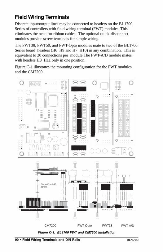
BL170090 s Field Wiring Terminals and DIN Rails
Field Wiring TerminalsDiscrete input/output lines may be connected to headers on the BL1700Series of controllers with field wiring terminal (FWT) modules. Thiseliminates the need for ribbon cables. The optional quick-disconnectmodules provide screw terminals for simple wiring.
The FWT38, FWT50, and FWT-Opto modules mate to two of the BL1700Series board headers (H6H9 and H7H10) in any combination. This isequivalent to 20 connections per module.The FWT-A/D module mateswith headers H8H11 only in one position.
Figure C-1 illustrates the mounting configuration for the FWT modulesand the CM7200.
Figure C-1. BL1700 FWT and CM7200 Installation
Battery
SCC
CM7200
R13
C2
R1
C4
R8
R9
R3
R6
R7
C5
R4
R5
R10
R2C3
C1
Standoff, to 4-40screws
FWT-A/DFWT-Opto FWT38

BL1700 Field Wiring Terminals and DIN Rails s 91
These four FWT styles described in this section are availablefrom Z-World. Your application may use a different arrange-ment than that shown in Figure C-1.
FWT38The FWT38 has 20 terminals in two groups with 10 terminals each. Eachgroup of terminals may be removed independently.
Table C-1 summarizes the specifications for the FWT38.
Figure C-2 provides the dimensions for the FWT38.
Figure C-2. FWT38 Dimensions
!
Table C-1. FWT38 Specifications
Parameter Specification
Total I/O Channels 16
Screw Terminal Pitch 3.81 mm
Maximum Wire Gauge 28-16 AWG
Quick-DisconnectCapability
Wiring banks can be unplugged from theboard separately (Phoenix Combicon typeconnection)
Wire Orientation Top-exiting wires
0.25 typ(6.4)
2.85(72.4)
~1.1
(28) ~0
.7(1
8)~0
.32
(8.1
)
0.12
5(3
.2)
0.92
5(2
3.5)
0.115 dia, 2x(2.9)

BL170092 s Field Wiring Terminals and DIN Rails
Figure C-3 shows the I/O channel assignments and pinouts for the FWT38.
Figure C-3. FWT38 Pinouts
FWT50The FWT50 provides 20 screw terminals. The terminal connectors arefixed to the FWT module and cannot be removed.
Table C-2 summarizes the specifications for the FWT50.
0001020304050607
GNDK
0809101112131415
GNDK
Bank AFWT38
Bank BFWT38
0001020304050607
GNDK
0809101112131415
GNDK
Table C-2. FWT50 Specifications
Parameter Specification
Total I/O Channels 16
Screw Terminal Pitch 5.00 mm
Maximum Wire Gauge 24-12 AWG
Quick-DisconnectCapability
Unplugs from the BL1700 board as a singleunit
Wire Orientation Side-exiting wires
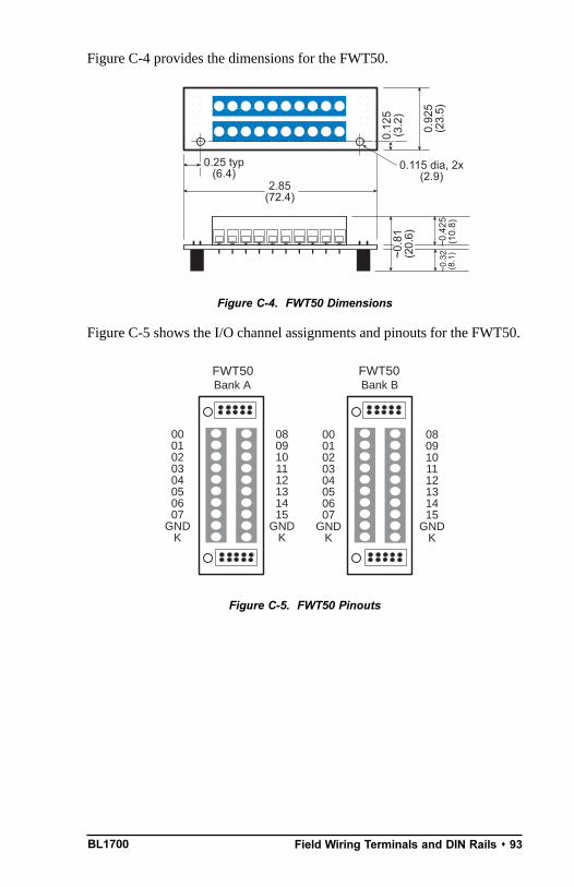
BL1700 Field Wiring Terminals and DIN Rails s 93
Figure C-4 provides the dimensions for the FWT50.
Figure C-4. FWT50 Dimensions
Figure C-5 shows the I/O channel assignments and pinouts for the FWT50.
Figure C-5. FWT50 Pinouts
0.25 typ(6.4)
2.85(72.4)
0.12
5(3
.2)
0.92
5(2
3.5)
~0.4
25(1
0.8)
~0.3
2(8
.1)
0.115 dia, 2x(2.9)
~0.8
1(2
0.6)
0809101112131415
GNDK
0001020304050607
GNDK
Bank AFWT50
Bank BFWT50
0001020304050607
GNDK
0809101112131415
GNDK
BL170094 s Field Wiring Terminals and DIN Rails
FWT-OptoThe FWT-Opto provides optical isolation to the input channels. TheFWT-Opto is used only for inputs, and is not used if the BL1700 banks areall configured as outputs. All 16 channels must be committed to inputswhen an FWT-Opto module is used.
Every four FWT-Opto inputs share a common return. Theexcitation resistors need to be pulled up to +5 V when theFWT-Opto module is used.
Table C-3 summarizes the specifications for the FWT-Opto.
The FWT-Opto module uses 4.7 kΩ input resistors to accommodate thelarge range of input voltages. This limits the input switching threshold to±9.5 V. These 4.7 kΩ input resistors need to be replaced with 1.2 kΩ inputresistors to handle smaller input voltages such as 5 V logic. If 0.125 Wresistors are used, this will limit the maximum input voltage to ±12.2 V.
Table C-3. FWT-Opto Specifications
Parameter Specification
Total Input Channels 16 optically isolated input channels only
Screw Terminal Pitch 3.81 mm
Maximum Wire Gauge 28-16 AWG
Quick-DisconnectCapability
Wiring banks can be unplugged from theboard separately (Phoenix Combicon typeconnection)
Wire Orientation Top-exiting wires
Input Protection Range 5 kV rms between input and output
Maximum Input Voltage ±40 V
Guaranteed InputSwitching Threshold
±9.5 V
!
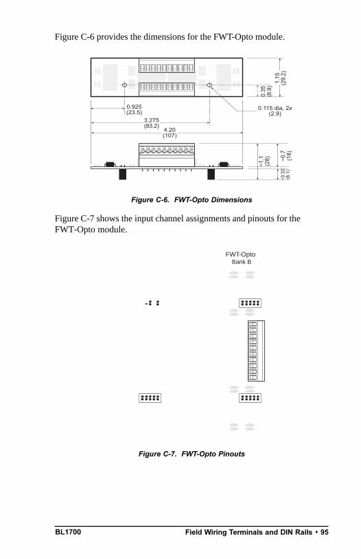
BL1700 Field Wiring Terminals and DIN Rails s 95
0.925(23.5)
3.275(83.2)
4.20(107)
0.115 dia, 2x(2.9)
0.35
(8.9
)1.
15(2
9.2)
~1.1
(28) ~0
.7(1
8)~0
.32
(8.1
)
Figure C-6 provides the dimensions for the FWT-Opto module.
Figure C-6. FWT-Opto Dimensions
Figure C-7 shows the input channel assignments and pinouts for theFWT-Opto module.
Figure C-7. FWT-Opto Pinouts
Bank BFWT-Opto
Bank A
FWT-OptoCOM300010203COM404050607

BL170096 s Field Wiring Terminals and DIN Rails
Figure C-8 shows an FWT-Opto optical isolation circuit.
Figure C-8. FWT-Opto Optical Isolation Circuit
The opto-isolated inputs share a common return in groups offour. The software channel assignments remain the same forBanks A and B.
00
10 kΩ
0110 kΩ
02
10 kΩ
02
10 kΩ
10 k10 k10 k10 k
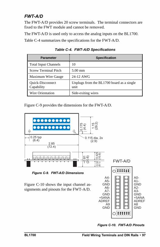
BL1700 Field Wiring Terminals and DIN Rails s 97
FWT-A/DThe FWT-A/D provides 20 screw terminals. The terminal connectors arefixed to the FWT module and cannot be removed.
The FWT-A/D is used only to access the analog inputs on the BL1700.
Table C-4 summarizes the specifications for the FWT-A/D.
Figure C-9 provides the dimensions for the FWT-A/D.
Figure C-10 shows the input channel as-signments and pinouts for the FWT-A/D.
Table C-4. FWT-A/D Specifications
Parameter Specification
Total Input Channels 10
Screw Terminal Pitch 5.00 mm
Maximum Wire Gauge 24-12 AWG
Quick-DisconnectCapability
Unplugs from the BL1700 board as a singleunit
Wire Orientation Side-exiting wires
A0-A1-GNDA2-A3-GND+5ANAADREFA8GND
A4-A5-
GNDA6-A7-
GND+5ANAADREF
A9GND
FWT-A/D
Figure C-10. FWT-A/D Pinouts
0.25 typ(6.4)
2.85(72.4)
0.17
5(4
.4)
~0.4
25(1
0.8)
~0.3
2(8
.1)
0.115 dia, 2x(2.9)
~0.8
1(2
0.6)
1.15
(29.
2)
Figure C-9. FWT-A/D Dimensions
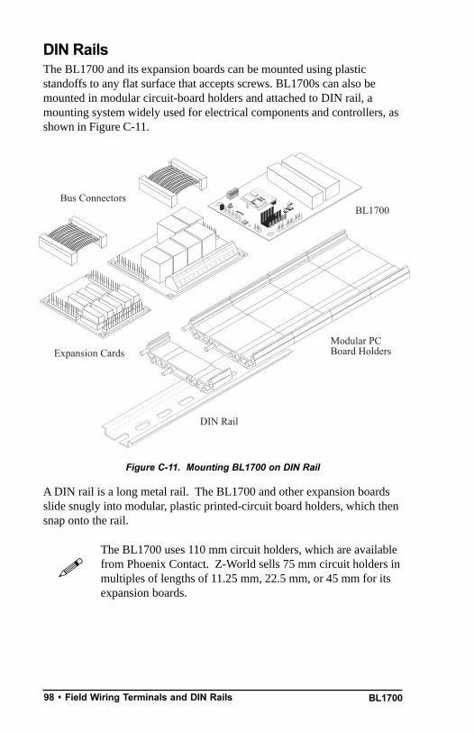
BL170098 s Field Wiring Terminals and DIN Rails
Bus ConnectorsBL1700
Modular PCBoard Holders
DIN Rail
Expansion Cards
DIN RailsThe BL1700 and its expansion boards can be mounted using plasticstandoffs to any flat surface that accepts screws. BL1700s can also bemounted in modular circuit-board holders and attached to DIN rail, amounting system widely used for electrical components and controllers, asshown in Figure C-11.
Figure C-11. Mounting BL1700 on DIN Rail
A DIN rail is a long metal rail. The BL1700 and other expansion boardsslide snugly into modular, plastic printed-circuit board holders, which thensnap onto the rail.
The BL1700 uses 110 mm circuit holders, which are availablefrom Phoenix Contact. Z-World sells 75 mm circuit holders inmultiples of lengths of 11.25 mm, 22.5 mm, or 45 mm for itsexpansion boards.
!

BL1700 Sinking and Sourcing Drivers s 99
APPENDIX D: SINKING AND
SOURCING DRIVERS

BL1700100 s Sinking and Sourcing Drivers
BL1700 Series Sinking and Sourcing OutputsThe BL1700 Series controllers are normally supplied with ULN2803sinking drivers. Figure D-1 shows a typical sinking driver output configu-ration.
Figure D-1. Sinking Driver Output
Figure D-2 shows the jumper configurations for a sinking driver output.
Figure D-2. Sinking Driver Jumper Configurations
Sourcing outputs are possible by replacing the factory-installed sinkingdriver chips with sourcing output drivers (UDN2985). The UDN2985sourcing driver chip is capable of sourcing a maximum of 75 mA peroutput.
ULN2803
K
ExternalLoad
FreewheelDiode
+DC
I # 500 mA/channel
Fly
back
Cur
rent
Pat
h
VS
AT #
1.6
V D
C
SINKING DRIVER JUMPER SETTINGS
H3
1357
2468
FD
Channels 0–7 Channels 8–15

BL1700 Sinking and Sourcing Drivers s 101
(
Figure D-3 shows a typical sourcing driver output.
Figure D-3. Sourcing Driver Output
Figure D-4 shows the jumper configurations for a sourcing driver output.
Figure D-4. Sourcing Driver Jumper Configurations
Z-World also offers all BL1700 Series controllers forquantity orders with factory-installed sourcing drivers.For ordering information, call your Z-World SalesRepresentative at (530) 757-3737.
H3
1357
2468
Channels 0–7 Channels 8–15
SOURCING DRIVER JUMPER SETTINGS
ExternalLoad
UDN2985
K
+DC
FreewheelDiode
VS
AT #
1.6
V D
C
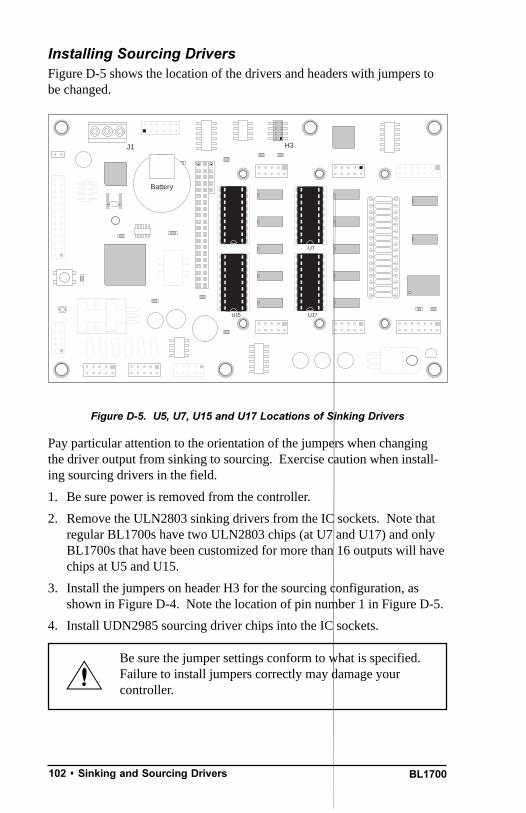
BL1700102 s Sinking and Sourcing Drivers
Installing Sourcing DriversFigure D-5 shows the location of the drivers and headers with jumpers tobe changed.
Figure D-5. U5, U7, U15 and U17 Locations of Sinking Drivers
Pay particular attention to the orientation of the jumpers when changingthe driver output from sinking to sourcing. Exercise caution when install-ing sourcing drivers in the field.
1. Be sure power is removed from the controller.
2. Remove the ULN2803 sinking drivers from the IC sockets. Note thatregular BL1700s have two ULN2803 chips (at U7 and U17) and onlyBL1700s that have been customized for more than 16 outputs will havechips at U5 and U15.
3. Install the jumpers on header H3 for the sourcing configuration, asshown in Figure D-4. Note the location of pin number 1 in Figure D-5.
4. Install UDN2985 sourcing driver chips into the IC sockets.
Be sure the jumper settings conform to what is specified.Failure to install jumpers correctly may damage yourcontroller.
Battery
H3J1
U17
U7
U15
U5

BL1700 Sinking and Sourcing Drivers s 103
(
TTL/CMOS OutputsZ-World also offers TTL- or CMOS-compatible outputs for the BL1700Series controllers. Input and output channels may be configured indepen-dently in any combination. However, the functionality of each input is notindependent; the inputs are still characterized in groups of four or eight.
Z-World offers all BL1700 Series controllers in quantitywith factory-installed TTL- or CMOS-compatible outputs.For ordering information, call your Z-World Sales Repre-sentative at (530) 757-3737.
Using Output DriversThe common supply for all eight channels supplied by a driver chip iscalled K, and is labeled as such on the BL1700s terminals. K must bepowered up to allow proper operation.
The K connection performs two vital functions to the high-voltage drivercircuitry on the BL1700.
1. K supplies power to driver circuitry inside the driver chip.
2. K also allows a diode internal to the driver chip to snub voltagetransients produced during the inductive kick associated with switchinginductive loads. (Relays, solenoids, and speakers are examples ofinductive loads.)
Long leads may present enough induction to also produce large potentiallydamaging voltage transients. The anodes of the protection diodes for eachchannel are common, and so only one voltage supply can be used for allhigh-voltage driver loads.
The following points summarize the functions of K.
K provides power to the driver chip circuitry.
K provides clamping for all high-voltage driver loads.
It is mandatory to connect K regardless of whether sourcing or sinking.
The loads supply must have a common ground with all other suppliesin your system.
All loads must use same supply voltage.
Refer to Figure D-6 and Figure D-7 when connecting K.
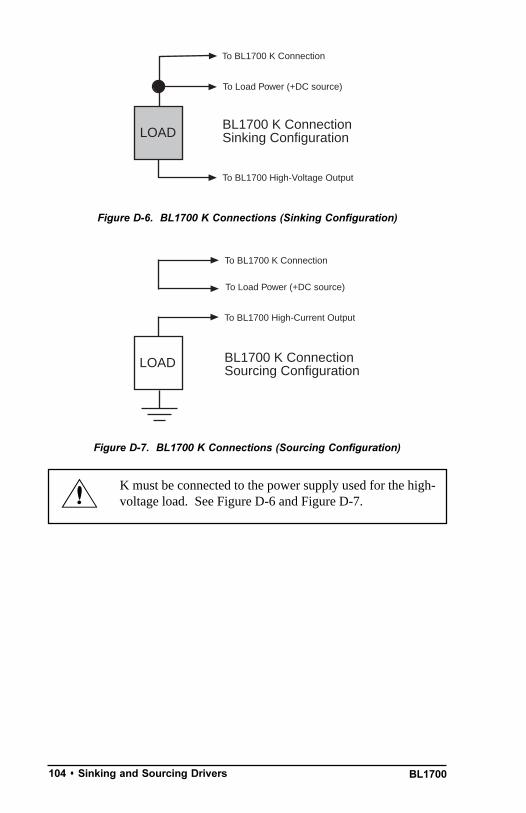
BL1700104 s Sinking and Sourcing Drivers
To BL1700 K Connection
To BL1700 High-Voltage Output
LOAD
To Load Power (+DC source)
BL1700 K ConnectionSinking Configuration
To BL1700 K Connection
To BL1700 High-Current Output
BL1700 K ConnectionSourcing Configuration
LOAD
To Load Power (+DC source)
Figure D-6. BL1700 K Connections (Sinking Configuration)
Figure D-7. BL1700 K Connections (Sourcing Configuration)
K must be connected to the power supply used for the high-voltage load. See Figure D-6 and Figure D-7.

BL1700 PLCBus s 105
APPENDIX E: PLCBUS
Appendix E provides the pin assignments for the PLCBus, describes theregisters, and lists the software drivers.
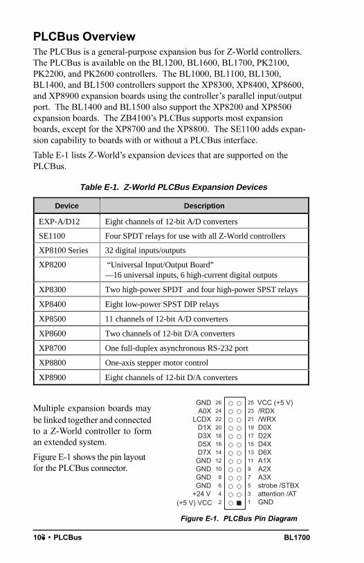
BL1700106 s PLCBus
PLCBus OverviewThe PLCBus is a general-purpose expansion bus for Z-World controllers.The PLCBus is available on the BL1200, BL1600, BL1700, PK2100,PK2200, and PK2600 controllers. The BL1000, BL1100, BL1300,BL1400, and BL1500 controllers support the XP8300, XP8400, XP8600,and XP8900 expansion boards using the controllers parallel input/outputport. The BL1400 and BL1500 also support the XP8200 and XP8500expansion boards. The ZB4100s PLCBus supports most expansionboards, except for the XP8700 and the XP8800. The SE1100 adds expan-sion capability to boards with or without a PLCBus interface.
Table E-1 lists Z-Worlds expansion devices that are supported on thePLCBus.
Multiple expansion boards maybe linked together and connectedto a Z-World controller to forman extended system.
Figure E-1 shows the pin layoutfor the PLCBus connector.
Table E-1. Z-World PLCBus Expansion Devices
Device Description
EXP-A/D12 Eight channels of 12-bit A/D converters
SE1100 Four SPDT relays for use with all Z-World controllers
XP8100 Series 32 digital inputs/outputs
XP8200 “Universal Input/Output Board”—16 universal inputs, 6 high-current digital outputs
XP8300 Two high-power SPDT and four high-power SPST relays
XP8400 Eight low-power SPST DIP relays
XP8500 11 channels of 12-bit A/D converters
XP8600 Two channels of 12-bit D/A converters
XP8700 One full-duplex asynchronous RS-232 port
XP8800 One-axis stepper motor control
XP8900 Eight channels of 12-bit D/A converters
24
13
6 58 7
10 912 1114 1316 1518 1720 1922 2124 2326 25
GNDD7XD5XD3XD1X
LCDXA0X
GND
GND attention /ATstrobe /STBXGNDA3XGNDA2XGNDA1X
/RDXVCC (+5 V)
D0X/WRX
D4XD2X
D6X
+24 V(+5 V) VCC
Figure E-1. PLCBus Pin Diagram

BL1700 PLCBus s 107
Two independent buses, the LCD bus and the PLCBus, exist on the singleconnector.
The LCD bus consists of the following lines.
LCDXpositive-going strobe. /RDXnegative-going strobe for read. /WRXnegative-going strobe for write. A0Xaddress line for LCD register selection. D0X-D7Xbidirectional data lines (shared with expansion bus).
The LCD bus is used to connect Z-Worlds OP6000 series interfaces or todrive certain small liquid crystal displays directly. Figure E-2 illustratesthe connection of an OP6000 interface to a controller PLCBus.
Figure E-2. OP6000 Connection to PLCBus Port
The PLCBus consists of the following lines.
/STBXnegative-going strobe.
A1XA3Xthree control lines for selecting bus operation.
D0XD3Xfour bidirectional data lines used for 4-bit operations.
D4XD7Xfour additional data lines for 8-bit operations.
/ATattention line (open drain) that may be pulled low by any device,causing an interrupt.
The PLCBus may be used as a 4-bit bus (D0XD3X) or as an 8-bit bus(D0XD7X). Whether it is used as a 4-bit bus or an 8-bit bus depends onthe encoding of the address placed on the bus. Some PLCBus expansioncards require 4-bit addressing and others (such as the XP8700) require8-bit addressing. These devices may be mixed on a single bus.
Yellow wireon top
PLCBus HeaderNote position of connector
relative to pin 1.
From OP6000KLB Interface CardHeader J2
Pin 1

BL1700108 s PLCBus
There are eight registers corresponding to the modes determined by buslines A1X, A2X, and A3X. The registers are listed in Table E-2.
Writing or reading one of these registers takes care of all the bus details.Functions are available in Z-Worlds software libraries to read from orwrite to expansion bus devices.
To communicate with a device on the expansion bus, first select a registerassociated with the device. Then read or write from/to the register. Theregister is selected by placing its address on the bus. Each device recog-nizes its own address and latches itself internally.
A typical device has three internal latches corresponding to the threeaddress bytes. The first is latched when a matching BUSADR0 is de-tected. The second is latched when the first is latched and a matchingBUSADR1 is detected. The third is latched if the first two are latched anda matching BUSADR2 is detected. If 4-bit addressing is used, then thereare three 4-bit address nibbles, giving 12-bit addresses. In addition, aspecial register address is reserved for address expansion. This address, ifever used, would provide an additional four bits of addressing when usingthe 4-bit convention.
If eight data lines are used, then the addressing possibilities of the busbecome much greatermore than 256 million addresses according to theconventions established for the bus.
Table E-2. PLCBus Registers
Register Address A3 A2 A1 Meaning
BUSRD0 C0 0 0 0 Read data, one way
BUSRD1 C2 0 0 1Read data, anotherway
BUSRD2 C4 0 1 0 Spare, or read data
BUSRESET C6 0 1 1Read this register toreset the PLCBus
BUSADR0 C8 1 0 0First address nibbleor byte
BUSADR1 CA 1 0 1Second addressnibble or byte
BUSADR2 CC 1 1 0Third address nibbleor byte
BUSWR CE 1 1 1 Write data
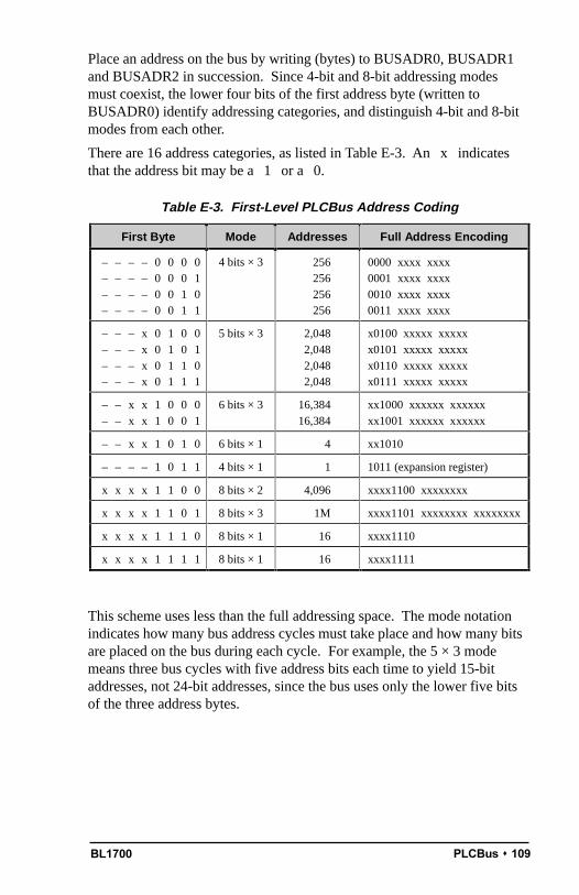
BL1700 PLCBus s 109
Place an address on the bus by writing (bytes) to BUSADR0, BUSADR1and BUSADR2 in succession. Since 4-bit and 8-bit addressing modesmust coexist, the lower four bits of the first address byte (written toBUSADR0) identify addressing categories, and distinguish 4-bit and 8-bitmodes from each other.
There are 16 address categories, as listed in Table E-3. An x indicatesthat the address bit may be a 1 or a 0.
This scheme uses less than the full addressing space. The mode notationindicates how many bus address cycles must take place and how many bitsare placed on the bus during each cycle. For example, the 5 × 3 modemeans three bus cycles with five address bits each time to yield 15-bitaddresses, not 24-bit addresses, since the bus uses only the lower five bitsof the three address bytes.
Table E-3. First-Level PLCBus Address Coding
First Byte Mode Addresses Full Address Encoding
– – – – 0 0 0 0– – – – 0 0 0 1– – – – 0 0 1 0– – – – 0 0 1 1
4 bits × 3 256256256256
0000 xxxx xxxx0001 xxxx xxxx0010 xxxx xxxx0011 xxxx xxxx
– – – x 0 1 0 0– – – x 0 1 0 1– – – x 0 1 1 0– – – x 0 1 1 1
5 bits × 3 2,0482,0482,0482,048
x0100 xxxxx xxxxxx0101 xxxxx xxxxxx0110 xxxxx xxxxxx0111 xxxxx xxxxx
– – x x 1 0 0 0– – x x 1 0 0 1
6 bits × 3 16,38416,384
xx1000 xxxxxx xxxxxxxx1001 xxxxxx xxxxxx
– – x x 1 0 1 0 6 bits × 1 4 xx1010
– – – – 1 0 1 1 4 bits × 1 1 1011 (expansion register)
x x x x 1 1 0 0 8 bits × 2 4,096 xxxx1100 xxxxxxxx
x x x x 1 1 0 1 8 bits × 3 1M xxxx1101 xxxxxxxx xxxxxxxx
x x x x 1 1 1 0 8 bits × 1 16 xxxx1110
x x x x 1 1 1 1 8 bits × 1 16 xxxx1111
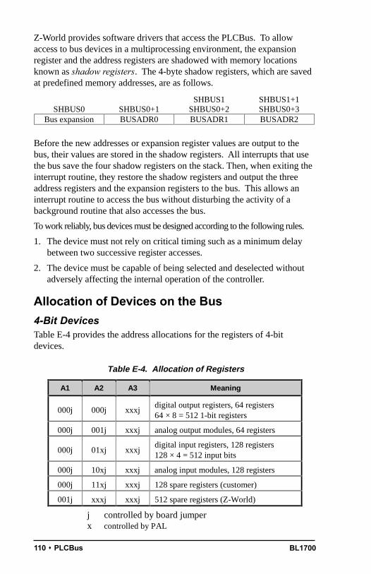
BL1700110 s PLCBus
Z-World provides software drivers that access the PLCBus. To allowaccess to bus devices in a multiprocessing environment, the expansionregister and the address registers are shadowed with memory locationsknown as shadow registers. The 4-byte shadow registers, which are savedat predefined memory addresses, are as follows.
Before the new addresses or expansion register values are output to thebus, their values are stored in the shadow registers. All interrupts that usethe bus save the four shadow registers on the stack. Then, when exiting theinterrupt routine, they restore the shadow registers and output the threeaddress registers and the expansion registers to the bus. This allows aninterrupt routine to access the bus without disturbing the activity of abackground routine that also accesses the bus.
To work reliably, bus devices must be designed according to the following rules.
1. The device must not rely on critical timing such as a minimum delaybetween two successive register accesses.
2. The device must be capable of being selected and deselected withoutadversely affecting the internal operation of the controller.
Allocation of Devices on the Bus
4-Bit DevicesTable E-4 provides the address allocations for the registers of 4-bitdevices.
SHBUS1 SHBUS1+1SHBUS0 SHBUS0+1 SHBUS0+2 SHBUS0+3
Bus expansion BUSADR0 BUSADR1 BUSADR2
Table E-4. Allocation of Registers
A1 A2 A3 Meaning
000j 000j xxxjdigital output registers, 64 registers64 × 8 = 512 1-bit registers
000j 001j xxxj analog output modules, 64 registers
000j 01xj xxxjdigital input registers, 128 registers128 × 4 = 512 input bits
000j 10xj xxxj analog input modules, 128 registers
000j 11xj xxxj 128 spare registers (customer)
001j xxxj xxxj 512 spare registers (Z-World)
j controlled by board jumperx controlled by PAL

BL1700 PLCBus s 111
Digital output devices, such as relay drivers, should be addressed withthree 4-bit addresses followed by a 4-bit data write to the control register.The control registers are configured as follows
bit 3 bit 2 bit 1 bit 0A2 A1 A0 D
The three address lines determine which output bit is to be written. Theoutput is set as either 1 or 0, according to D. If the device exists on thebus, reading the register drives bit 0 low. Otherwise bit 0 is a 1.
For digital input, each register (BUSRD0) returns four bits. The readregister, BUSRD1, drives bit 0 low if the device exists on the bus.
8-Bit DevicesZ-Worlds XP8700 and XP8800 expansion boards use 8-bit addressing.Refer to the XP8700 and XP8800 manual.
Expansion Bus SoftwareThe expansion bus provides a convenient way to interface Z-Worldscontrollers with expansion boards or other specially designed boards. Theexpansion bus may be accessed by using input functions. Follow thesuggested protocol. The software drivers are easier to use, but are lessefficient in some cases. Table E-5 lists the libraries.
Table E-5. Dynamic C PLCBus Libraries
Library Needed Controller
DRIVERS.LIB All controllers
EZIOTGPL.LIB BL1000
EZIOLGPL.LIB BL1100
EZIOMGPL.LIB BL1400, BL1500
EZIOPLC.LIB BL1200, BL1600, PK2100, PK2200, ZB4100
EZIOPLC2.LIB BL1700
PBUS_TG.LIB BL1000
PBUS_LG.LIB BL1100, BL1300
PLC_EXP.LIB BL1200, BL1600, PK2100, PK2200

BL1700112 s PLCBus
There are 4-bit and 8-bit drivers. The 4-bit drivers employ the followingcalls.
void eioResetPlcBus()
Resets all expansion boards on the PLCBus. When using this call,make sure there is sufficient delay between this call and the first accessto an expansion board.
LIBRARY: EZIOPLC.LIB, EZIOPLC2.LIB, EZIOMGPL.LIB.
void eioPlcAdr12( unsigned addr )
Specifies the address to be written to the PLCBus using cyclesBUSADR0, BUSADR1, and BUSADR2.
PARAMETER: addr is broken into three nibbles, and one nibble iswritten in each BUSADRx cycle.
LIBRARY: EZIOPLC.LIB, EZIOPLC2.LIB, EZIOMGPL.LIB.
void set16adr( int adr )
Sets the current address for the PLCBus. All read and write operationsaccess this address until a new address is set.
PARAMETER: adr is a 16-bit physical address. The high-ordernibble contains the value for the expansion register, and the remainingthree 4-bit nibbles form a 12-bit address (the first and last nibbles mustbe swapped).
LIBRARY: DRIVERS.LIB.
void set12adr( int adr )
Sets the current address for the PLCBus. All read and write operationsaccess this address until a new address is set.
PARAMETER: adr is a 12-bit physical address (three 4-bit nibbles)with the first and third nibbles swapped.
LIBRARY: DRIVERS.LIB.
void eioPlcAdr4( unsigned addr )
Specifies the address to be written to the PLCBus using only cycleBUSADR2.
PARAMETER: addr is the nibble corresponding to BUSADR2.
LIBRARY: EZIOPLC.LIB, EZIOPLC2.LIB, EZIOMGPL.LIB.
BL1700 PLCBus s 113
void set4adr( int adr )
Sets the current address for the PLCBus. All read and write operationsaccess this address until a new address is set.
A 12-bit address may be passed to this function, but only the last fourbits will be set. Call this function only if the first eight bits of theaddress are the same as the address in the previous call to set12adr.
PARAMETER: adr contains the last four bits (bits 811) of thephysical address.
LIBRARY: DRIVERS.LIB.
char _eioReadD0( )
Reads the data on the PLCBus in the BUSADR0 cycle.
RETURN VALUE: the byte read on the PLCBus in the BUSADR0cycle.
LIBRARY: EZIOPLC.LIB, EZIOPLC2.LIB, EZIOMGPL.LIB.
char _eioReadD1( )
Reads the data on the PLCBus in the BUSADR1 cycle.
RETURN VALUE: the byte read on the PLCBus in the BUSADR1cycle.
LIBRARY: EZIOPLC.LIB, EZIOPLC2.LIB, EZIOMGPL.LIB.
char _eioReadD2( )
Reads the data on the PLCBus in the BUSADR2 cycle.
RETURN VALUE: the byte read on the PLCBus in the BUSADR2cycle.
LIBRARY: EZIOPLC.LIB, EZIOPLC2.LIB, EZIOMGPL.LIB.
char read12data( int adr )
Sets the current PLCBus address using the 12-bit adr, then reads fourbits of data from the PLCBus with BUSADR0 cycle.
RETURN VALUE: PLCBus data in the lower four bits; the upper bitsare undefined.
LIBRARY: DRIVERS.LIB.
BL1700114 s PLCBus
char read4data( int adr )
Sets the last four bits of the current PLCBus address using adr bits 811, then reads four bits of data from the bus with BUSADR0 cycle.
PARAMETER: adr bits 811 specifies the address to read.
RETURN VALUE: PLCBus data in the lower four bits; the upper bitsare undefined.
LIBRARY: DRIVERS.LIB.
void _eioWriteWR( char ch)
Writes information to the PLCBus during the BUSWR cycle.
PARAMETER: ch is the character to be written to the PLCBus.
LIBRARY: EZIOPLC.LIB, EZIOPLC2.LIB, EZIOMGPL.LIB.
void write12data( int adr, char dat )
Sets the current PLCBus address, then writes four bits of data to thePLCBus.
PARAMETER:
BL1700 PLCBus s 115
void set8adr( long address )
Sets the current address on the PLCBus. All read and write operationswill access this address until a new address is set.
PARAMETER: address contains the last eight bits of the physicaladdress in bits 1623. A 24-bit address may be passed to this function,but only the last eight bits will be set. Call this function only if the first16 bits of the address are the same as the address in the previous call toset24adr.
LIBRARY: DRIVERS.LIB.
int read24data0( long address )
Sets the current PLCBus address using the 24-bit address, then readseight bits of data from the PLCBus with a BUSRD0 cycle.
RETURN VALUE: PLCBus data in lower eight bits (upper bits 0).
LIBRARY: DRIVERS.LIB.
int read8data0( long address )
Sets the last eight bits of the current PLCBus address using address bits1623, then reads eight bits of data from the PLCBus with a BUSRD0cycle.
PARAMETER: address bits 1623 are read.
RETURN VALUE: PLCBus data in lower eight bits (upper bits 0).
LIBRARY: DRIVERS.LIB.
void write24data( long address, char data )
Sets the current PLCBus address using the 24-bit address, then writeseight bits of data to the PLCBus.
PARAMETERS: address is 24-bit address to write to.
data is data to write to the PLCBus.
LIBRARY: DRIVERS.LIB.
void write8data( long address, char data )
Sets the last eight bits of the current PLCBus address using address bits1623, then writes eight bits of data to the PLCBus.
PARAMETERS: address bits 1623 are the address of the PLCBusto write.
data is data to write to the PLCBus.
LIBRARY: DRIVERS.LIB.

BL1700116 s PLCBus
Blank
BL1700 Serial Interface Board 2 s 117
APPENDIX F:
SERIAL INTERFACE BOARD 2
Appendix F provides technical details and baud rate configuration data forZ-Worlds Serial Interface Board 2 (SIB2).
118 s Serial Interface Board 2 BL1700
IntroductionThe SIB2 is an interface adapter used to program the BL1700. The SIB2is contained in an ABS plastic enclosure, making it rugged and reliable.The SIB2 enables the BL1700 to communicate with Dynamic C via theZ180s clocked serial I/O (CSI/O) port, freeing the BL1700s serial portsfor use by the application during programming and debugging.
The SIB2s 8-pin cable plugs into the target BL1700s processor throughan aperture in the backplate, and a 6-conductor RJ-12 phone cableconnects the SIB2 to the host PC. The SIB2 automatically selects its baudrate to match the communication rates established by the host PC (9600,19,200, or 57,600 bps). However, the SIB2 determines the hosts commu-nication baud rate only on the first communication after reset. To changebaud rates, change the COM baud rate, reset the target BL1700 (whichalso resets the SIB2), then select Reset Target from Dynamic C.
Chapter 2 provides detailed information on connecting theSIB2 to the BL1700.
The SIB2 receives power and resets from the target BL1700 via the 8-pinconnector J1. Therefore, do not unplug the SIB2 from the target BL1700while power is applied. To do so could damage both the BL1700 and theSIB2; additionally, the target may reset.
Never connect or disconnect the SIB2 with power appliedto the BL1700.
The SIB2 consumes approximately 60 mA from the +5 V supply. Thetarget-system current consumption therefore increases by this amountwhile the SIB2 is connected to the BL1700.
$
BL1700 Serial Interface Board 2 s 119
Top View
Side View
2.25(57.2)
12.0(305)
3.60(91.4)
0.8(20)
1.525(38.7) 1.625
(41.3)
External DimensionsFigure F-1 illustrates the external dimensions for the SIB2.
Figure F-1. SIB2 External Dimensions

120 s Serial Interface Board 2 BL1700
Blank
BL1700 Advanced Topics s 121
APPENDIX G: ADVANCED TOPICS
Appendix G provides more advanced information to help the user needingto implement special applications. The following topics are included.
Power Management
Memory Map
Interrupts
Flash EPROM
Pulse-Width Modulation Software

BL1700122 s Advanced Topics
Power Management
Power Failure Detection CircuitryFigure G-1 shows the power fail detection circuitry of the BL1700.
Figure G-1. BL1700 Power-Failure Detection Circuit
Power Failure Sequence of EventsFigure G-2 shows the events that occur as the input power fails.
Figure G-2. Power Failure Sequence
1N581
1N5230
DCIN
CM7200PFI
Power SupplyCircuitry uP Supervisor
4.7 kΩ1%
51 kΩ1%
PFI
VCC = +5 V
1.0
2.0
9.0
8.0
7.0
6.0
5.0
4.0
3.0
I
UnregulatedDC
Regulated+5 V
691Asserts PFO
691AssertsRESET
691 CeasesOperation
tH
Power Fails
Time
CSlope = C/-I
Dropout Voltage
10.0
11.0
14.0
13.0
12.0
15.0
Inpu
t Vol
tage
(V
)

BL1700 Advanced Topics s 123
1. The power-management IC triggers a power-fail /NMI (nonmaskableinterrupt) when the DC input voltage falls within the range of 14.44 Vto 14.72 V DC.
2. At some point, the raw input voltage will not be sufficient for theregulator to provide 5 V DC to the BL1700 due to dropout voltage. Atthat point the regulated output begins to drop. The power-managementIC triggers a reset when the regulated 5 V DC output falls within therange of 4.50 V to 4.75 V DC. This causes the power-fail routine to beinvoked. The power-fail routine can be used to store important statedata.
Use a power supply with a large capacitance if you need toincrease the holdup time. This will provide additional time forthe BL1700 to execute a safe shutdown.
3. The power management IC switches power for the time/date clock andSRAM to the lithium backup battery when the regulated voltage fallsbelow the battery voltage of approximately 3 V DC.
4. The power management IC keeps the system in reset until the regulatedvoltage drops below 1 V DC. At this point the power-management ICceases operating. By this time, the portion of the circuitry not battery-backed has already ceased functioning.
The ratio of your power supplys output capacitors value to your circuitscurrent draw determines the actual holdup time.
A situation similar to a continuous low input (brownout) can occur if thepower supply is overloaded. For example, when a high-current devicesuch as a relay turns ON, the raw voltage supplied to the BL1700 may dipbelow 14.44 V DC. The interrupt routine performs a shutdown. Thisshutdown turns off the relay, clearing the problem. However, if the causeof the overload persists, the system oscillates, alternately experiencing anoverload and then resetting. Using a power supply with a sufficiently largecurrent capacity will correct this problem.
If you remove the power cable abruptly from the BL1700 side, then onlythe capacitors on the board provide power, reducing computing time to afew microseconds. These times can vary considerably depending onsystem configuration and loads on the BL1700 power supplies.
The interval between the power-failure detection and entry to the power-failure interrupt routine is approximately 100 µs, or less if Dynamic C/NMI communication is not in use.
Tip

BL1700124 s Advanced Topics
Table G-1. Z180 Internal I/O Registers Addresses 0x00–0x3F
Address Name Description
0x00 CNTLA0 Serial Channel 0, Control Register A
0x01 CNTLA1 Serial Channel 1, Control Register A
0x02 CNTLB0 Serial Channel 0, Control Register B
0x03 CNTLB1 Serial Channel 1, Control Register B
0x04 STAT0 Serial Channel 0, Status Register
0x05 STAT1 Serial Channel 1, Status Register
0x06 TDR0 Serial Channel 0, Transmit Data Register
0x07 TDR1 Serial Channel 1, Transmit Data Register
0x08 RDR0 Serial Channel 0, Receive Data Register
0x09 RDR1 Serial Channel 1, Receive Data Register
0x0A CNTR Clocked Serial Control Register
0x0B TRDR Clocked Serial Data Register
0x0C TMDR0L Timer Data Register Channel 0, low
0x0D TMDR0H Timer Data Register Channel 0, high
0x0E RLDR0L Timer Reload Register Channel 0, low
0x0F RLDR0H Timer Reload Register Channel 0, high
0x10 TCR Timer Control Register
0x11–0x13 — Reserved
0x14 TMDR1L Timer Data Register Channel 1, low
0x15 TMDR1H Timer Data Register Channel 1, high
0x16 RLDR1L Timer Reload Register Channel 1, low
0x17 RLDR1H Timer Reload Register Channel 1, high
continued…
Memory Map
Input/Output Select MapThe Dynamic C library functions IBIT, ISET and IRES in the BIOS.LIBlibrary allow bits in the I/O registers to be tested, set, and cleared. The I/Oaddresses need to be 16-bit addresses.
Z180 Internal Input/Output Register Addresses 0x00-0x3FThe internal registers for the I/O devices built into to the Z180 processoroccupy the first 40 (hex) addresses of the I/O space. These addresses arelisted in Table G-1.
BL1700 Advanced Topics s 125
Table G-1. Z180 Internal I/O Registers Addresses 0x00–0x3F (concluded)
Address Name Description
0x18 FRC Free-running counter
0x19–0x1F — Reserved
0x20 SAR0L DMA source address Channel 0, low
0x21 SAR0H DMA source address Channel 0, high
0x22 SAR0B DMA source address Channel 0, extra bits
0x23 DAR0L DMA destination address Channel 0, low
0x24 DAR0H DMA destination address Channel 0, high
0x25 DAR0B DMA destination address Channel 0, extra bits
0x26 BCR0L DMA Byte Count Register Channel 0, low
0x27 BCR0H DMA Byte Count Register Channel 0, high
0x28 MAR1L DMA Memory Address Register Channel 1, low
0x29 MAR1H DMA Memory Address Register Channel 1, high
0x2A MAR1BDMA Memory Address Register Channel 1, extrabits
0x2B IAR1L DMA I/O Address Register Channel 1, low
0x2C IAR1H DMA I/O Address Register Channel 1, high
0x2D — Reserved
0x2E BCR1L DMA Byte Count Register Channel 1, low
0x2F BCR1H DMA Byte Count Register Channel 1, high
0x30 DSTAT DMA Status Register
0x31 DMODE DMA Mode Register
0x32 DCNTL DMA/WAIT Control Register
0x33 IL Interrupt Vector Low Register
0x34 ITC Interrupt/Trap Control Register
0x35 — Reserved
0x36 RCR Refresh Control Register
0x37 — Reserved
0x38 CBR MMU Common Base Register
0x39 BBR MMU Bank Base Register
0x3A CBAR MMU Common/ Bank Area Register
0x3B–0x3D — Reserved
0x3E OMCR Operation Mode Control Register
0x3F ICR I/O Control Register

BL1700126 s Advanced Topics
Table G-2. BL1700 External I/O Device Registers
Address Name R/W Function
0x4000 EN485A W D0 = RS-485 Channel 1 Enable
0x4040 ENDI1 R D0-D7 = Digital Input[00–15]
0x4040 TE485B W D0 = RS-485 Channel B TransmitEnable
0x4042 ENDI2 R D0-D7 = Digital Input[16–31]
0x4042 TE485A W D0 = RS-485 Channel A TransmitEnable
0x40C0 ADEOC R D0 = ADC end of conversion
0x40D0 ADOUT R D0 = ADC output
0x40D0 ADIN W D2 = ADC instruction
0x40D0 ADCS W D1 = ADC chip select
0x40D0 ADCLK W D0 = ADC clock
0x40E0 LCD R/W PLCBus LCD line
0x40F0 /STB R/W PLCBus strobe
0x4100 /ENHV1 W Digital Output [00–07]
0x4108 /ENHV2 W Digital Output [08–15]
0x4110 /ENHV3 W Digital Output [16–23]
0x4118 /ENHV4 W Digital Output [24–31]
0x4120 SCC R/W Serial Channel B, Control
0x4121 R/W Serial Channel A, Control
0x4122 R/W Serial Channel B, Data
0x4123 R/W Serial Channel A, Data
0x4142 LED W D0 = LED status
0x417F R D7 = Run/Program Mode, D6–D0 = ID
$
BL1700 Peripheral AddressesTable G-2 lists the addresses that control I/O devices external to the Z180processor.
Refer to the Zilog or Hitachi Users Manual for more informa-tion about the Z80180/Z180 or the 64180 MPU internal I/Oregister map.
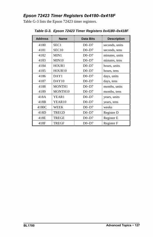
BL1700 Advanced Topics s 127
Epson 72423 Timer Registers 0x41800x418FTable G-3 lists the Epson 72423 timer registers.
Table G-3. Epson 72423 Timer Registers 0x4180–0x418F
Address Name Data Bits Description
4180 SEC1 D0–D7 seconds, units
4181 SEC10 D0–D7 seconds, tens
4182 MIN1 D0–D7 minutes, units
4183 MIN10 D0–D7 minutes, tens
4184 HOUR1 D0–D7 hours, units
4185 HOUR10 D0–D7 hours, tens
4186 DAY1 D0–D7 days, units
4187 DAY10 D0–D7 days, tens
4188 MONTH1 D0–D7 months, units
4189 MONTH10 D0–D7 months, tens
418A YEAR1 D0–D7 years, units
418B YEAR10 D0–D7 years, tens
4180C WEEK D0–D7 weeks
418D TREGD D0–D7 Register D
418E TREGE D0–D7 Register E
418F TREGF D0–D7 Register F

BL1700128 s Advanced Topics
(
$
$
InterruptsThe BL1700 provides user access totwo level-sensitive interrupts. The in-terrupts are shared with onboard pe-ripherals such as the PLCBus port andserial channels. If these peripherals arenot used, then external devices may usethese interrupts. Header H1 providesconnections to the /INT0 and /INT1interrupt lines of the Z180 processoraccording to the pinout shown in Fig-ure G-3. Header J4 provides jumperconnections to allow external connec-tion to the /INT0 and /INT1 signals.
See Chapter 3, BL1700 Hardware, for information onjumper settings for header J4.
Z-World can install a header at header location H1 in produc-tion quantities. For more information, call your Z-World SalesRepresentative at (530) 757-3737.
Interrupts can be enabled or disabled by including the following com-mands in your code.
Interrupt 0 ON (enabled)~ outport(ITC,inport(ITC) | 1)
Interrupt 1 ON (enabled)~ outport(ITC,inport(ITC) | 2)
Interrupt 0 OFF (disabled)~ outport(ITC,inport(ITC) & 0xfe)
Interrupt 1 OFF (disabled)~ outport(ITC,inport(ITC) & 0xfd)
Interrupt Service RoutinesInterrupt service routines are packets of code that the processor jumps toand executes when it receives an interrupt request.
Refer to the Dynamic C manuals for instructions on writinginterrupt service routines.
Refer to the Zilog Z80180/Z180 Users Manual (availablefrom Z-World) for complete details on using Z180 interrupts.
10
H1
1 2
3 4
5 6
7 8
9
/DCDB
/SYNCA
/SYNCB
/DREQ0
/DREQ1
/DTRB
/RTXCA
/RTXCB
/TRXCA
/TRXCB
11 12/INT0 /INT1
Figure G-3. Pinouts forOptional Header H1
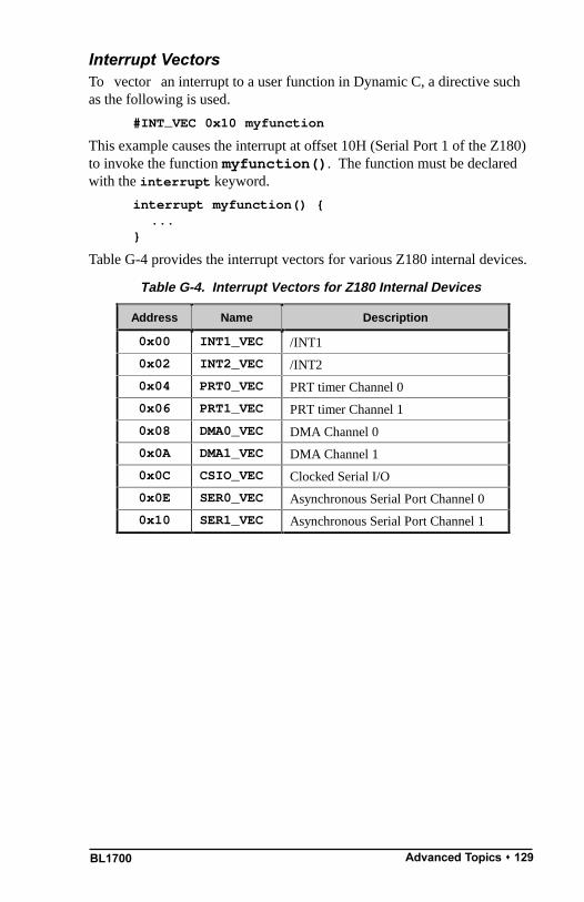
BL1700 Advanced Topics s 129
Interrupt VectorsTo vector an interrupt to a user function in Dynamic C, a directive suchas the following is used.
#INT_VEC 0x10 myfunction
This example causes the interrupt at offset 10H (Serial Port 1 of the Z180)to invoke the function myfunction(). The function must be declaredwith the interrupt keyword.
interrupt myfunction() ...
Table G-4 provides the interrupt vectors for various Z180 internal devices.
Table G-4. Interrupt Vectors for Z180 Internal Devices
Address Name Description
0x00 INT1_VEC /INT1
0x02 INT2_VEC /INT2
0x04 PRT0_VEC PRT timer Channel 0
0x06 PRT1_VEC PRT timer Channel 1
0x08 DMA0_VEC DMA Channel 0
0x0A DMA1_VEC DMA Channel 1
0x0C CSIO_VEC Clocked Serial I/O
0x0E SER0_VEC Asynchronous Serial Port Channel 0
0x10 SER1_VEC Asynchronous Serial Port Channel 1

BL1700130 s Advanced Topics
Table G-5 lists the interrupt priorities.
Jump VectorsJump vectors are similar to interrupt vectors, except that instead of loadingthe address of the interrupt routine from the interrupt vector, these inter-rupts cause a jump directly to the address of the vector, which contains ajump instruction to the interrupt routine. This is an example of a jumpvector.
0x66 nonmaskable power-failure interrupt
Because nonmaskable interrupts can be used for Dynamic C communica-tion, the interrupt vector for power failure is normally stored just in frontof the Dynamic C program. Store a vector there by using this compilerdirective.
#JUMP_VEC NMI_VEC name
The Dynamic C communication routines jump to this vector when a powerfailure causes the NMI rather than a serial interrupt.
Table G-5. Interrupt Priorities
Interrupt Priorities
(Highest Priority) Trap (Illegal Instruction)
NMI (Nonmaskable Interrupt)
INT 0 (Maskable Interrupt, Level 0)
INT 1 (Maskable Interrupt, Level 1)
INT 2 (Maskable Interrupt, Level 2)
PRT Timer Channel 0
PRT Timer Channel 1
DMA Channel 0
DMA Channel 1
Clocked Serial I/O
Serial Port 0
(Lowest Priority) Serial Port 1

BL1700 Advanced Topics s 131
Flash EPROM
Simulated EEPROMThe BL1700 uses a section of the flash EPROM to simulate EEPROM.The size of the simulated EEPROM is 512 bytes (not Kbytes). Locations0x02 through 0x3D are used to store the analog input calibration constants.The rest of the simulated EEPROM is free for use by the application.These functions are used to read/write from/to the simulated EEPROM.
int ee_rd( int address )
Reads and returns data from flash EPROM storage location address.The function returns 1 if it is unable to read data.
LIBRARY: BIOS.LIB
int ee_wr( int address, int data )
Writes data to flash EPROM storage location address. The functionreturns 1 if it is unablae to write data.
LIBRARY: BIOS.LIB

BL1700132 s Advanced Topics
Other Flash EPROM Software int WriteFlash( unsigned long physical_addr,
char *buf, int count )
Writes count number of bytes pointed to by buf to the flash EPROMabsolute data location physical_adr. Allocate the data location bydeclaring the byte arrays as initialized arrays or declare an initializedxdata array. If byte array is declared, conert logical memory tophysical memory with phy_adr(array). For initialized xdata, youcan pass the array name directly.
PARAMETERS: physical_adr is the absolute data location in theflash EPROM.
*buf is a pointer to the bytes to write.
count is the number of bytes to write.
RETURN VALUES:
0 if WriteFlash is okay.
1 if the flash EPROM is not in use.
2 if physical_addr is inside the BIOS area.
3 if physical_addr is within the symbol area or the simulatedEEPROM area.
4 if WriteFlash times out.
LIBRARY: DRIVERS.LIB
Flash EPROM is rated for 10,000 writes. In practice, flashEPROM has performed for up to 100,000 writes. Z-Worldrecommends that any writes to the flash EPROM be made bythe programmer rather than automatically by the software tomaximize the life of the flash EPROM.
!
BL1700 Advanced Topics s 133
Pulse-Width Modulation (PWM) Software
PWM Addressing DetailThe driver of the PWM on the BL1700 is fairly complicated. This isbecause it uses the clock output from communication port 1 (CKA1) todrive the request line DMA Channel 0 in edge detection mode. The simpleinterface previously described in Chapter 4 provides PWM support foroutput 0 to output 3. If the application requires more PWM channels orrequire specific frequencies or precision, the application engineer mayneed to make trade-offs.
This section describes how PWM channels are driven, as well as how tocustomize PWM resource allocation to compromise number of modulatedchannels, frequency, and resolution.
1. Determine the number of channels, frequency, and resolution.
A pulse-width modulated waveform has a frequency and a resolution. Thefrequency states how many times the pattern repeats itself in a second(Hz). The resolution states how many divisions within one waveform canbe resolved (distinguished). As a collection, the PWM driver also needs toknow the total number of channels to be pulse-width modulated. Thecalculations in this section are made with the assumption that all channelshave the same frequency and resolution.
The clock output from communication port 1 (CKA1) must have afrequency,
f1 = N
ch × f
w × R
w ,
where which f1 is the frequency of CKA1, N
ch is the number of channels
PW modulated, fw is the frequency of each channel, and R
w is the resolu-
tion in number of divisions per wave.
For example, the driver interface, _eioSetupAO1st, makes the followingassumptions.
Nch
= 4
f1 = 76,800 Hz
Rw = 256
Consequently, fw = 76,800 Hz/(4 × 256) = 75 Hz.
2. Declare storage for the WPB (waveform pattern buffer).
Memory must be allocated to store the waveform pattern.
BL1700134 s Advanced Topics
3. Set up the waveform.
The PWM functions use the Z180s built-in DMA mechanism to transferPWM edges from memory to the high-current ports at specific timeintervals. Each edge is a byte whose least-significant four bits select oneof the high-current outputs, output 0 through output 6. The least signifi-cant bit is a 1 to turn the specified port on (rising PWM edge) or a 0 toturn the specified port off (falling PWM edge). Edges for the channelsbeing pulse-width modulated are then grouped into composite transitions.
Each composite transition is a series of edges, each representing onepossible transition for an individual channel. For example, if output 0 andoutput 1 are the only pulse-width modulated channels, a compositetransition consists of two bytes. The first byte specifies a possible transi-tion for channel output 0. The second byte specifies a possible transitionfor channel output 1.
Let us assume the first byte in the composite transition corresponds tooutput 0, and the second byte corresponds to output 1.
The composite PWM waveform is a series of composite transitions (CTs)that specify the duty cycle of the pulse-width modulated channels. Forexample, if output 0 is to have a 0.375 duty cycle, output 1 is to be at 0.75duty cycle, and the resolution is 8 divisions per cycle, a simple wave formwould be as follows.
CT1: turn on output 0, turn on output 1.
CT2: do nothing.
CT3: do nothing.
CT4: turn off output 0.
CT5: do nothing.
CT6: do nothing.
CT7: turn off output 1.
CT8: do nothing.
Go back to CT1.

BL1700 Advanced Topics s 135
Outputting the byte 0x01 turns on output 0, 0x00 turns off output 0, 0x03turns on output 1, and 0x02 turns off output 1. The byte 0x0E is an no-op and it does nothing. The composite transitions (with no-ops) can betranslated into the following byte sequence to be sent to the I/O address0x4100.
CT1: 0x01, 0x03
CT2: 0x0E, 0x0E
CT3: 0x0E, 0x0E
CT4: 0x00, 0x0E
CT5: 0x0E, 0x0E
CT6: 0x0E, 0x0E
CT7: 0x0E, 0x02
CT8: 0x0E, 0x0E
Go back to CT1
The equivalent byte stream (contents in the waveform pattern buffer) is arepeating pattern of the following.
0x01, 0x03, 0x0E, 0x0E, 0x0E, 0x0E, 0x00, 0x0E,0x0E, 0x0E, 0x0E, 0x0E, 0x0E, 0x02, 0x0E, 0x0E
The driver library provides a function, dmapwmSetBuf, that allows theapplication engineer to modify the content of the waveform pattern buffer.
4. Set up the clock.
The DMA device transfer from memory to I/O port address 0x4100 isdriven by falling edges on signal /DREQ0. Since /DREQ0 is connected toCKA1 (the clock output of communication channel 1), the communicationspeed of communication channel 1 determines how frequently the DMAdevice transfer memory to I/O. Each transfer corresponds to one edge inthe previous section.
Refer to the Zilog users manual for more information on howto set up the CKA1 frequency for the Z80180/Z180 or to theHitachi users manual for the 64180 MPU.
The driver does include a function, dmapwmInit, that sets up the fre-quency of CKA1. The function is described later in this appendix.
The PWM interface sets up CKA1 to clock at 76,800 Hz in the call_eioSetupAO1st().
$
BL1700136 s Advanced Topics
5. Refresh the DMA counter and source address.
The DMA device does not automatically reload the counter and sourceaddress registers when the specified amount of bytes is transferred. Whenthe DMA device finishes transferring the specified amount of bytes, itstops and optionally causes an interrupt. In other words, the PWMwaveform is abruptly ended when the DMA finishes.
To overcome this limitation, the application program must periodicallyrefresh the counter and source address registers of the DMA device. Therefresh should check whether the counter is less than a critical number. Ifso, both the counter and the source address registers must be rewound toa previous state (a larger counter value and a corresponding lower sourceaddress).
Note that the PWM waveforms cannot be disrupted while it is refreshingthe registers. In other words, the previous state to which the refreshroutine restores must be phase synchronized with the PWM waveforms atthe moment.
The driver library provides a refresh routine, _eioBrdAORf, to refresh theDMA counter and source address registers. _eioBrdAORf() can becalled from a preemptive task or from the main program. The refreshroutine must be called frequently enough so that the DMA counter neverreaches 0. The following inequality states the requirement.
fr ≥ f
1/(l
wpb/2)
in which fr is the refresh frequency, f
1 is the frequency of CKA1, and l
wpb is
the total length of the waveform pattern buffer.
For example, _eioSetupAO1st() sets up f1 = 76,800Hz and l
wpb = 4096.
As a result, the application engineer must ensure fr ≥ 37.5 Hz.
6. Changing duty cycles.
Once the PWM waveforms are up and running, the application may needto change the duty cycles for the channel(s). This poses two problems.First, the change should only be done to the channel that needs a change ofduty cycle, all other channels should remain the same. Second, the changemust become effective phase synchronized with the current waveform.
The solution to the first problem depends on how the edges are repre-sented. In particular, it depends on whether the no-op edges are used. Ifthe no-op edges are used, changing duty cycle is a matter of moving theedges that are not no-op. For example, in our example in the set up the

BL1700 Advanced Topics s 137
waveform section, if we wish to change the duty cycle of output 0 to0.25, we change the waveform from
0x01, 0x03, 0x0E, 0x0E, 0x0E, 0x0E, 0x00, 0x0E,0x0E, 0x0E, 0x0E, 0x0E, 0x0E, 0x02, 0x0E, 0x0E
to
0x01, 0x03, 0x0E, 0x0E, 0x00, 0x0E, 0x0E, 0x0E,0x0E, 0x0E, 0x0E, 0x0E, 0x0E, 0x02, 0x0E, 0x0E
The underlined edges are the only ones affected.
Of course, the waveform pattern buffer may have the pattern repeatedmany times. Each occurrence of the pattern in the buffer must be modifiedin the same manner.
However, although the use of no-op edges seems to be compute-timeinexpensive, it does require the application to maintain the location of thenon-no-op edges. In other words, besides the waveform pattern buffer, theapplication program must maintain a duty cycle variable for each channel.
Recall that the second problem of changing the duty cycle is the require-ment for the change to be phase synchronized to the current waveform.Many of the involved issues are similar to those of refreshing the DMAcounter and pointer. The driver software library provides the functiondmapwmSwBuf to switch waveform pattern buffers.
PWM SoftwareThe functions shown below are second level functions that allow morePWM outputs. They are also more complex and require a morein-depth understanding of PWM and DMA generation. These functionsare located in EZIODPWM.LIB.
void dmapwmSetBuf ( char *pBufStart,char bufLength256,unsigned step, char outChar )
Formats part of the waveform pattern buffer for DMA-driven PWM.
In other words, dmapwmSetBuf does the following: starting at theaddress pointed to by pBufStart, for bufLength256 many 256-bytepages, change every step bytes to outChar.
PARAMETERS: pBufStart points to the first byte to be formatted.Note that pBufStart does not always have to point to a 256-bytealigned address.
bufLength256 is the length of the buffer, including the overflow area.
step is the number of bytes to skip between outputting outChar.
outChar is the actual bytes to send to the I/O address.

BL1700138 s Advanced Topics
void dmapwmSwBuf ( unsigned newBuf256 )
In order to facilitate all-or-none duty cycle transitions, you should usetwo buffers. While one buffer is being used by the DMA mechanism togenerate the PWM output, modify the other buffer for the new PWMpattern. When the new buffer is ready, this function should be called toswitch to use the buffer at the address pointed to by newBuf256 in256-byte units.
char *dmapwmBufBeg ( char *bufPtr )
The buffer used by the PWM mechanism starts at 256-byte boundaries.Normal data definition declarations such as
char buffer[0x2000]
start at byte boundaries. dmapwmBufBeg returns a character pointerthat points to the first 256-byte aligned root address larger than orequal to the parameter bufPtr.
void dmapwmInit( unsigned phyBuffer256,unsigned bufSize256, unsigned resSize256,unsigned ioAddr, char cka1rate )
Initializes the DMA PWM mechanism.
When the function returns, CKA1 of communication port 1 generatesclock pulses at cka1rate * 19.2 kHz to /DREQ0. DMA Channel 0would then perform memory to I/O transfer for each clock pulse fallingedge.
PARAMETERS: phyBuffer256 is the 256 byte aligned physicaladdress of the buffer in 256-byte units. In general, if the buffer isdefined as an array in root memory (that is, of type (char *)), thefollowing expression should be passed to this parameter
(unsigned)((xmadr(buffer)+255)>>8)
in which buffer is a pointer of type (char *) to the array.
bufsize256 is the size of the buffer, in 256 byte units. This sizeshould not include the overflow area.
resSize256 is the size of the overflow area in 256 byte units.
ioAddr is the port to which the DMA should transfer memory content.
cka1rate is the clock rate generated by CKA1 in 19.2 kHz units.Allowed numbers are 2, 4, and 8.

BL1700 Advanced Topics s 139
Sample ProgramBL17PWM1.C and BL17PWM2.C are sample programs which show how touse the pulse width modulation feature using the functions listed above.They can be found in the Dynamic C SAMPLES\BL17XX directory.
The PWM functions use the Z180s built-in DMA hard-ware. Using this DMA-driven PWM limits the communica-tion speed of the Z180s Serial Port 1 to 4800 bps, and theZ180 runs effectively at least 8% slower. In addition youmust ensure your application calls _eioBrdAORf at leastevery 25 ms to refresh the drivers period.
If necessary, call Z-World Technical Support at(530)757-3737 for assistance.

BL1700140 s Advanced Topics
Blank

BL1700 Battery s 141
APPENDIX H: BATTERY
Appendix H provides information about the onboard lithium backupbattery.

BL1700142 s Battery
Battery Life and Storage ConditionsThe battery on the BL1700 controller will provide at least 9,000 hours ofbackup time for the onboard real-time clock and static RAM. However,backup time longevity is affected by many factors, including the amount oftime the controller is unpowered and the static RAM size. Most systemsare operated on a continuous basis, with the battery supplying power to thereal-time clock and the static RAM during power outages and/or duringroutine maintenance. The time estimate reflects the shelf life of a lithiumion battery with occasional use rather than the ability of the battery topower the circuitry full time.
The battery has a capacity of 190 mA·h. At 25°C, the real-time clock draws3 µA when idle, and the 32K SRAM draws 2 µA. If the BL1700 wereunpowered 100 percent of the time, the battery would last 38, 000 hours(4.3 years).
To maximize the battery life, the BL1700 should be stored at roomtemperature in the factory packaging until field installation. Take care thatthe BL1700 is not exposed to extreme temperature, humidity, and/orcontaminants such as dust and chemicals.
To ensure maximum battery shelf life, follow proper storage procedures.Replacement batteries should be kept sealed in the factory packaging atroom temperature until installation. Protection against environmentalextremes will help maximize battery life.
Replacing Soldered Lithium BatteryUse the following steps to replace the battery.
1. Locate the three pins on the bottom side of the printed circuit boardthat secure the battery to the board.
2. Carefully de-solder the pins and remove the battery. Use a soldersucker to clean up the holes.
3. Install the new battery and solder it to the board. Use only a PanasonicBR23251HG or its equivalent.

BL1700 Battery s 143
Battery Cautions Caution (English)
There is a danger of explosion if the battery is incorrectly replaced.Replace only with the same or equivalent type recommended by themanufacturer. Dispose of used batteries according to the manufactur-ers instructions.
Warnung (German)
Explosionsgefahr durch falsches Einsetzen oder Behandein derBatterie. Nur durch gleichen Typ oder vom Hersteller empfohlenenErsatztyp ersetzen. Entsorgung der gebrauchten Batterien gemäb denAnweisungen des Herstellers.
Attention (French)
Il y a danger dexplosion si la remplacement de la batterie est incorrect.Remplacez uniquement avec une batterie du même type ou dun typeéquivalent recommandé par le fabricant. Mettez au rebut les batteriesusagées conformément aux instructions du fabricant.
Cuidado (Spanish)
Peligro de explosión si la pila es instalada incorrectamente. Reemplacesolamente con una similar o de tipo equivalente a la que el fabricanterecomienda. Deshagase de las pilas usadas de acuerdo con lasinstrucciones del fabricante.
Waarschuwing (Dutch)
Explosiegevaar indien de batterij niet goed wordt vervagen.Vervanging alleen door een zelfde of equivalent type als aanbevolendoor de fabrikant. Gebruikte batterijen afvoeren als door de fabrikantwordt aangegeven.
Varning (Swedish)
Explosionsfära vid felaktigt batteribyte. Använd samma batterityp elleren likvärdigt typ som rekommenderas av fabrikanten. Kassera använtbatteri enligt fabrikantens instruktion.

BL1700144 s Battery
Blank
Index s 145BL1700
INDEX
Symbols
/AT ........................................... 107/DREQ0 ................................... 138/INT0 ....................................... 128/INT1 ....................................... 128
configuration .......................... 55/RDX........................................ 107/STBX ...................................... 107/WRX ....................................... 1074-bit bus operations .. 107, 108, 1105 × 3 addressing mode ............. 1098-bit bus operations .. 107, 109, 111
A
A/D converter ............................ 55internal test voltages .............. 46power-down mode ................. 47
A0X ......................................... 107A1X, A2X, A3X ............. 107, 108AdcMode .................................... 68addresses
BL1700 peripheral ............... 126EEPROM (simulated) .......... 131encoding............................... 109modes ................................... 109PLCBus ....................... 108, 109processor registers ............... 126
analog inputs ....................... 38, 67bias resistors .......................... 40calibrating .............................. 44calibration constants .............. 69conditioned ..................... 38, 39conditioned channels ............. 40data format ............................. 68drift ........................................ 45drivers .................................... 67excitation resistors ................. 46external connections .............. 47
analog inputs (continued)gain
bias resistors ............... 38, 39component tolerance ... 42, 45deviation ............................ 41
gain resistors .......................... 40initializing .............................. 67input range ...................... 38, 41low-pass filter ........................ 45op-amps .......................... 39, 40performance ........................... 43reading ................................... 67sample program ..................... 69setting up ......................... 39, 40software ................................. 67unconditioned ................. 38, 46
attention line ............................ 107
B
background routine .................. 110Bank A ................................ 59, 61Bank B ................................ 59, 61battery
cautions ................................ 142replacing .............................. 142
bidirectional data lines ............. 107BL1700 ...................................... 12
connecting to PC .................... 19mounting ................................ 98subsystems ............................. 27
BL17AIN.C ................................ 69BL17DIO.C ......................... 60, 62BL17PWM1.C ........................... 139BL17PWM2.C ........................... 139BL17PWM4.C ............................. 66bus
control registers ....................111digital inputs .........................111
BL1700146 s Index
bus (continued)expansion ..................... 106111
4-bit drivers ..................... 1128-bit drivers ..................... 114addresses .......................... 110devices ..................... 110, 111functions .................. 112115rules for devices ............... 110software drivers ................111
LCD ..................................... 107operations
4-bit ................ 107, 108, 1108-bit ......................... 107, 111
BUSADR0 ...................... 108, 109BUSADR1 ...................... 108, 109BUSADR2 ...................... 108, 109BUSADR3 ...................... 114, 115BUSRD0 .................. 111113, 115BUSRD1 .......................... 111, 112BUSWR ................................... 112
C
CE compliance ........................... 16CM7200 .............................. 27, 28CMOS outputs ......................... 103communication
and Dynamic C ...................... 21serial .................................... 124
Compilesample program ..................... 22
connectors26-pin PLCBus
pin assignments ................ 106core module ........................ 27, 28customization ............................. 14
D
D/A converter ............................ 55D0XD7X................................ 107DCIN ......................................... 21default jumper settings ............... 81Development Kit ........................ 15
packing list ............................. 18
digital I/O ................................... 55digital inputs .............................. 31
addresses ................................ 60Bank A ................................... 29Bank B ................................... 29connecting to ................... 30, 47Field Wiring Terminals ... 30, 47frequency response ................ 85input current ........................... 85logic threshold ....................... 31low-pass filter ........................ 31operating range ...................... 31operating voltage ................... 85opto isolation .................. 30, 47pull-downs ............................. 31pull-ups .................................. 31reading ............................ 59, 60sample program ..................... 60software ................................. 59specifications ......................... 85
digital outputs ............................ 34addresses ................................ 62Bank A ................................... 34Bank B ................................... 34connecting to .......................... 35high-voltage driver specifications
........................................... 87PWM ..................................... 63sample program ..................... 62software ................................. 61writing .................................... 61
dimensionsBL1700 .................................. 79FWT-A/D ............................... 97FWT-Opto .............................. 95FWT38 ................................... 91FWT50 ................................... 93SIB2 ..................................... 119
DIN rail ...................................... 98DIP relays ................................ 106display
liquid crystal ........................ 107DMA
and PWM ............................... 66
Index s 147BL1700
dmapwmBufBeg ....................... 138dmapwmInit .................. 135, 138dmapwmSetBuf ....................... 137dmapwmSwBuf ......................... 138drivers ........................................ 58
expansion bus .......................1114-bit .................................. 1128-bit .................................. 114
relay ......................................111sourcing
installation ....................... 102DRIVERS.LIB ..........................111Dynamic C ................................. 12
will not start ........................... 75
E
ee_rd ...................................... 131ee_wr ...................................... 131EEPROM (simulated)
addresses .............................. 131software .......................... 72, 76
eioBrdACalib ......................... 69eioBrdAI .................................. 67eioBrdAO .................................. 65eioBrdAORf .................... 66, 136eioBrdDI .................................. 59eioBrdDO .................................. 61eioBrdInit ............................. 67eioPlcAdr12 ......................... 112eioReadD0 .............................. 113eioReadD1 .............................. 113eioReadD2 .............................. 113eioResetPlcBus ................... 112eioSetupAO1st .............. 66, 135eioWriteWR ........................... 114electrical specifications .............. 78environmental specifications ..... 78EPROM
flash .............................. 27, 131Exp-A/D12............................... 106expansion boards
reset ...................................... 112
expansion bus .................. 1061114-bit drivers ......................... 1128-bit drivers ......................... 114addresses .............................. 110devices ......................... 110, 111digital inputs .........................111functions ...................... 112115rules for devices ................... 110software drivers ....................111
expansion register .................... 110EZIOBL17.LIB ......................... 58EZIOLGPL.LIB ........................111EZIOMGPL.LIB ........................111EZIOPL2.LIB ..........................111EZIOPLC.LIB ..........................111EZIOTGPL.LIB ........................111
F
features ....................................... 13Field Wiring Terminals . 30, 47, 89
installation ............................. 91flash EPROM .................... 27, 131flexibility.................................... 14function libraries ...................... 108FWT. See Field Wiring TerminalsFWT-A/D
pinouts ................................... 97specifications ......................... 97
FWT-Optooptical isolation circuit .......... 96pinouts ................................... 95specifications ......................... 94
FWT38pinouts ................................... 92specifications ......................... 91
FWT50pinouts ................................... 93specifications ......................... 92
H
H1 ............................................ 128H10 .............................. 30, 35, 47
BL1700148 s Index
H11 ............................................ 47H12 ............................................ 51H13 ............................................ 51H14 ............................................ 51H15 ............................................ 51H2 .............................................. 34H3 .............................................. 34H4 ................................ 19, 21, 24H6 ................................ 30, 35, 47H7 ................................ 30, 35, 47H8 .............................................. 47H9 ................................ 30, 35, 47headers
H1 ........................................ 128H10 .......................... 30, 35, 47H11 ........................................ 47H12 ................................. 19, 51H13 ........................................ 51H14 ........................................ 51H15 ........................................ 51H2 .......................................... 34H3 .......................................... 34H4 ............................ 19, 21, 24H6 ............................ 30, 35, 47H7 ............................ 30, 35, 47H8 .......................................... 47H9 ............................ 30, 35, 47J1 .................................... 19, 21J2 .................................... 31, 49J3 ........................................... 31J4 .................... 49, 51, 55, 128J7 ........................................... 51J8 .................................... 37, 49
high-voltage driversK .......................................... 103specifications ......................... 87
high-voltage outputs .................. 34
I
I/O expansion ............................. 55inport .... 60, 112, 113, 115, 124input voltage ............................ 123
inputs/outputsdevices ................................. 124map ...................................... 124space .................................... 124
interrupt service routines ......... 128interrupt vectors ....................... 129interrupts ......................... 107, 110
/INT0 ................................... 128/INT1 ................................... 128power failure ........................ 123routines ................................ 110
ISR. See interrupt service routines
J
J1 ........................................ 19, 21J2 ........................................ 31, 49J3 ............................................... 31J4 ........................ 49, 51, 55, 128J7 ............................................... 51J8 ........................................ 37, 49jump vectors ............................ 130jumper settings
/DREQ0 ................................. 37J8 ....................................... 37
/INT1J4 ....................................... 55
Bank Adigital inputs ...................... 32digital outputs .................... 36H2 ...................................... 36J2 ....................................... 32
Bank Bdigital inputs ...................... 33digital outputs .................... 35H3 ...................................... 35J3 ....................................... 33
default settings ....................... 81serial channel configuration . 49, 50
J2 ....................................... 49J4 ....................................... 50J8 ................................ 49, 50
Index s 149BL1700
jumper settings (continued)termination resistors ............... 53
J4 ....................................... 53J7 ....................................... 53
K
K .............................................. 103
L
LCD ......................................... 107LCD bus ................................... 107LCDX ...................................... 107LED ........................................... 72
turning on and off .................. 72libraries ...................................... 58
function ................................ 108liquid crystal display ................ 107lithium battery .......................... 142
M
mechanical dimensions .............. 79mechanical specifications .......... 78memory
read-only .............................. 131modes
addressing ............................ 109changing ................................. 25operating ................................ 24program .................................. 24run .......................................... 24standalone .............................. 26
mounting .................................... 98
O
operating modes ......................... 24optical isolation circuit .............. 96outport .. 61, 112, 113, 115, 124outputs
CMOS .................................. 103sourcing ............................... 100TTL ...................................... 103
P
peripheral addresses ................. 126pinouts
analog inputs .......................... 47H11 .................................... 47H8 ...................................... 47
digital I/O ............................... 30Bank A ............................... 30Bank B ............................... 30H10 .................................... 30H6 ...................................... 30H7 ...................................... 30H9 ...................................... 30
FWT-A/D ............................... 97FWT-Opto .............................. 95FWT38 ................................... 92FWT50 ................................... 93level-sensitive interrupts ...... 128
H1 .................................... 128serial communication headers 54
H12 .................................... 54H13 .................................... 54H14 .................................... 54H9 ...................................... 54
PLCBus ... 55, 106108, 110, 11126-pin connector
pin assignments ................ 1064-bit operations ........... 107, 1098-bit operations ........... 107, 109addresses ..................... 108, 109configuration .......................... 55expansion boards ................... 55external connections .............. 55memory-mapped I/O register 108operating modes ..................... 55reading data ......................... 108relays
DIP ................................... 106drivers ...............................111
writing data .......................... 108power
SIB2 ..................................... 118

BL1700150 s Index
power failuredetection circuit ................... 122interrupt ............................... 123reset ...................................... 123sequence of events ............... 122software .......................... 72, 76
power supplyconnecting ....................... 19, 21
processor register addresses .... 126program mode ............................ 24programming cable .................... 19PWM .................................. 37, 63
addressing ............................ 133advanced programming ....... 133buffers .................................. 138DMA refresh .......................... 66duty cycle ............................... 65initialization .................. 66, 138sample program ..................... 66sample programs .................. 139software
complex ........................... 137waveform pattern buffer ...... 137
R
RAM .......................................... 27read12data ........................... 113read24data ........................... 115read4data .............................. 114read8data .............................. 115reading data on the PLCBus ..........
................................ 108, 113real-time clock ........................... 27
software .......................... 72, 76registers
Z180 ..................................... 124relay outputs .............................. 55reset .......................................... 123
expansion boards ................. 112software .......................... 72, 76
RJ-12........................................ 118RS-232 communication ............. 48
RS-485 communication ...... 48, 70software ................................. 71terminating resistors ............... 51
run mode .................................... 24
S
sample programsanalog input ........................... 69BL17FLSH.C ......................... 22digital inputs .......................... 60digital outputs ........................ 62PWM ............................ 66, 139serial communication ............. 71
SCC ..................................... 48, 71sccSw485 .................................. 71SE1100..................................... 106select PLCBus address ............. 112serial channels ............................ 48
BL1720 .................................. 71BL1730 .................................. 71Channel 0 ............................... 48Channel 1 ............................... 48Channel A .............................. 48Channel B .............................. 48configuration .......................... 49drivers .................................... 71networking ............................. 51operating modes ..................... 49RS-485 ............................ 51, 70software ................................. 71
serial communication ............... 124DCD ....................................... 48DTR ....................................... 48external connections .............. 51sample program ..................... 71signals .................................... 51synchronous communication ... 48
serial communication controller ........................................ 48, 71
Serial Interface Board 2 .... 20, 118baud rate .............................. 118dimensions ........................... 119power ................................... 118
Index s 151BL1700
set12adr ................................ 112set16adr ................................ 112set24adr ................................ 114set4adr .................................. 113set8adr .................................. 115shadow registers ....................... 110sinking drivers ........................... 34
specifications ......................... 87software .............................. 15, 58
libraries ................................ 108sourcing drivers ......................... 34
specifications ......................... 87sourcing outputs ....................... 100specifications ............................. 77
electrical ................................ 78environmental ........................ 78FWT-A/D ............................... 97FWT-Opto .............................. 94FWT38 ................................... 91FWT50 ................................... 92mechanical ............................. 78
standalone mode ........................ 26standard models ......................... 14stepper motor control ................. 55subsystems ................................. 27switchLED ................................ 72
T
time/date clockregisters ................................ 127
timers ....................................... 124troubleshooting .......................... 73
board resets ............................ 76cables ..................................... 74grounding ............................... 74LCD connected to PLCBus port
........................................... 74PC COM ports ....................... 74PWM ..................................... 76
TTL outputs ............................. 103
U
UDN2985 .................................. 34ULN2803 ................................... 34
W
watchdog timer .......................... 27software .......................... 72, 76
write12data ......................... 114write24data ......................... 115write4data ........................... 114write8data ........................... 115WriteFlash ........................... 132writing data on the PLCBus ...........
................................ 108, 114
X
XP8100 .................................... 106XP8200 .................................... 106XP8300 .................................... 106XP8400 .................................... 106XP8500 .................................... 106XP8600 .................................... 106XP8700 .................. 106, 107, 111XP8800 ........................... 106, 111XP8900 .................................... 106
Z
Z180internal I/O registers ............ 124
z1Sw485 .................................... 71

BL1700152 s Index
Blank

Part No. 019-0048Revision E
Printed in U.S.A.
Z-World, Inc.2900 Spafford Street
Davis, California 95616-6800 USA
Telephone:Facsimile:Web Site:
E-Mail:
(530) 757-3737(530) 753-5141http://www.z w [email protected]