Embed Size (px)
Citation preview

Determinação Estrutural de Superfícies via
Difração de Fotoelétrons
Abner de SiervoInstituto de Física - Unicamp
http://www.ifi.unicamp.br/gfs

Tópicos• Introdução e Motivação
• Aspectos Experimentais e teóricos de Difração de Fotoelétrons (PED)
• Exemplos para Determinação Estrutural usando PED
•Perspectivas para PED e PH no LNLS

1 - IntroduçãoPorque Estudar Superfícies ?
A superfície é uma interface entre dois meios, muito comumna natureza:
• Solido-gás ; sólido-líqüido; sólido-sólido; sólido-vácuo; líqüido-gás.
• Grande relevância na Indústria: catálise, armazenamento de dados, microeletrônica, fotônica, tribologia, adesão, embalagens, proteção (corrosão/oxidação), biônica, ligas-2D, etc.

1.1 - Quais são as informações importantes ?Conhecer a estrutura eletrônica e arranjo geométrico dos átomos presentes na superfície pode ser a chave para se compreender melhor as propriedades físico-químicas de um material
Sempre estamos interessados em saber:
- identidade química, concentração, posições dos átomos, tipo de ligação, densidade de estados,energia total do sistema, etc.
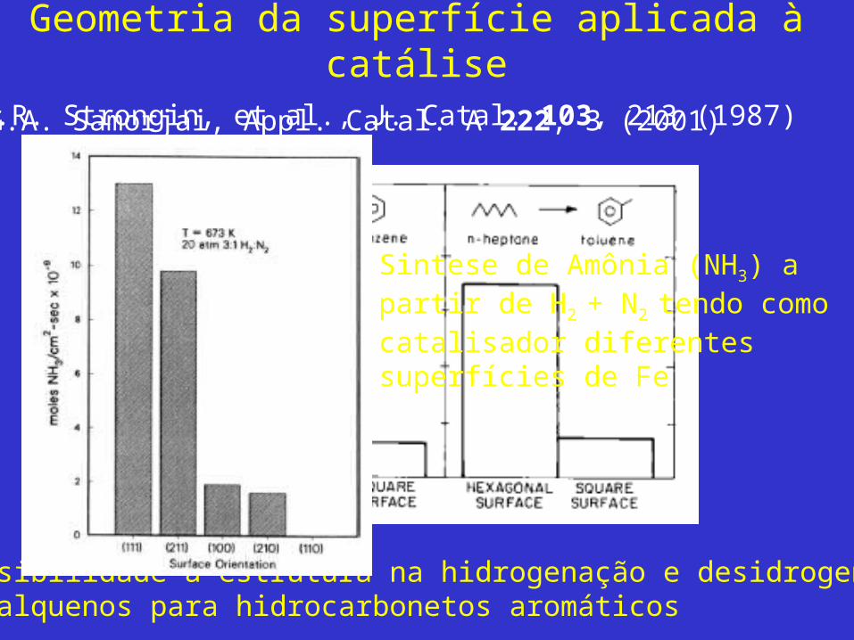
Geometria da superfície aplicada à catálise
Sensibilidade à estrutura na hidrogenação e desidrogenaçãode alquenos para hidrocarbonetos aromáticos
G.A. Samorjai, Appl. Catal. A 222, 3 (2001)
Sintese de Amônia (NH3) a partir de H2 + N2 tendo como catalisador diferentes superfícies de Fe
D.R. Strongin, et al., J. Catal. 103, 213 (1987)

2D Alloy : Au on Ni(111) for n-butane conversion
A) 0.02 ML of Au B) 0.07 ML of Au
DFT calculated adsorption energy for C atoms on Ni(111) in two cases :clean Ni(111) and substitute some Ni for Au.
n-butane conversion by Ni and Au/Ni-supported catalyst
Besenbacher et al. Science, 279 (1998)

Quais técnicas podem ser utilizadas ?
• As espectroscopias de fotoelétrons são bastante apropriadas para o estudo da estrutura eletrônica de superfície (XPS, UPS, AES)
• E para a determinação estrutural de superfície?

Técnicas Experimentais e Teóricas
11mm2 2 - 1mm- 1mm22 Único átomoÚnico átomo ( 300( 300Å ) - Å ) - 1mm1mm22
Resolução Resolução LateralLateral
5-20 5-20 ÅÅMajorit. DOS Majorit. DOS 1 camada1 camada
5-40 5-40 ÅÅProfundidadeProfundidade
Não Não diretamentediretamente
Comulmente Comulmente NãoNão
SimSimElemento/Elemento/QuímicaQuímica
Longo Longo ( >100( >100Å )Å )
curto, longo e curto, longo e desordenadodesordenado
Curto ( < 10Curto ( < 10Å )Å )Tipo de Tipo de ordemordem
LEEDLEEDSTMSTMPED e PED PED e PED HolographyHolography
•RHEED dinâmica de crescimento• DFT, Monte Carlo, Dinâmica Molecular ...

Definições e Nomenclatura para superfícies ordenadas
Espaço Real Espaço Recíproco
2
1
2221
1211
2
1
aa
mmmm
b
b
21
21
bmbnR
amanR
)ˆ(
ˆ2
;)ˆ(
ˆ2
12
1*2
21
2*1
naanaa
naanaa

Determinação qualitativa da geometria da superfície por LEED
?Espaço Real
Espaço Recíproco
oRPd 3033)111(

Photoelectron Diffraction (PED)
?Espaço Real
h DiretoEspalhamentoMúltiplo

Teoria Difração de Fotoelétrons
rdrrUrrGer
solução
UkEVm
rkik
3.2/3
2222
)()(),(41
)2(1)(
:2
2
0),,( j
jkI
Espalhamento de um pacote de onda:
rerf
rerVHV
mpH
ikr
k
rki
k )ˆ()2(
1~)(2
.
2/30
2
Método das Funções de Green:
E.Marzbacher,”Quantum Mechanics”, Cap.11

emiter0R
1R
2nR
1nR
detectornR
• Diagonal PW scattering t- matrix :
• Matrizes radiais :
• Propagador de partícula livre:
)exp()sin( lll it
)( );,( ;,,)(, RRkmlLRLGRLG LL
Espalhamento Múltiplo
infEll lrlmiKinif,.,,
2)(),,(
, 1min,,
imemissor ilfl n
hocafLLlilflilin GtmkI

Characteristics of Photoelectron DiffractionAdvantages:• Element Specific, Chemistry Specific• Short range order probe ( < 20 Å)• Sub-surface Sensitivity• Angular Momentum and Spin Dependence• Selective excitation controlling photon energy and polarized light (Linear , Circular Dichroism)• Direct Structure 3 D atomic images from holographic analysis
Disadvantages:• Expensive • Most powerful with Synchrotron• Slow : hours to days ( conventional ); minutes to hours ( powerful SR)• May be very depending of theoretical models
( multiple scattering calculation)
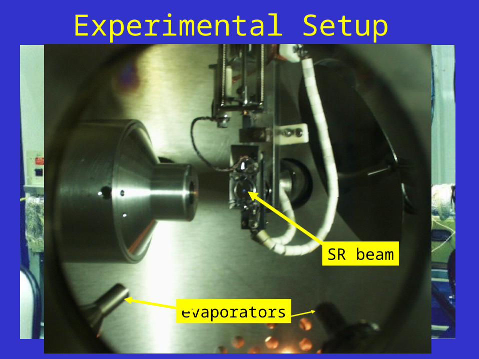
Experimental Setup
evaporators
SR beam

Some Examples of Surface Structure Determined by PD at LNLS
• Clean Metal Surface : Pd (111)
• Random Surface Alloys : Pd on Cu (111) and Cu on
Pd(111)
• Ordered 2D Alloy : Pd(111) - Sb 3033 R

Pd 3d: PD experimentClean Pd(111)
d12 (%) d23(%)MSCD +1.2 -1.5DFT +1.8 +0.8LEED1 +1.3 -1.31 H. Ohtani et al., Surf. Sci. 187, 372 (1987)
~400 XPS
MSCD code ( Y. Chen and M. Van Hove) http://electron.lbl.gov/
Pd 3d: MSCD Theory
iiec
ic
iec
ic
aR 22
2
Ra=0.23

Random surface Alloy of Pd on Cu(111) after anneal.
E0=90 eV ( clean Cu(111) )
E0=90 eV (PdCu alloy)
Pd 3d experimental PDPd 3d MSCD Theory• structure at 20o indicate Pd diffusion up to 3rdlayer• Best fit to : 20:70:20 % of Pd in the 1st, 2nd and 3rd layers respectively.• 5% expansion of the first interlayer distance• 2% contraction of second interlayer distance•E.A. Soares et. al Surface Science 497 (2002)205• A. de Siervo et. al Surface Science 504C(2002) 215
20o

~ 1ML Cu on Pd(111) after anneal. 600K
Cu 3p: Exp.• Random Alloy
• Very good (1x1)LEED pattern
• ~ 100% Cu 1st layer
• ~ very little Cu in the 2nd layer and none in the 3rd layer.
Small Diffusion !!!
Cu 3p: theoryRa=0.13
A.de Siervo et al. (unpublished)

~ 3ML Cu on Pd(111) Annealed to ~ 1000 KPd 3d: Experimental
Pd 3d: MSCD Theory
Cu 3p: Experimental
Cu 3p: MSCD Theory
• Random Alloy
• > 90 % Cu 1st layer
• ~ 75 % Cu 2nd layer (Cu3Pd)
• No diffusion to 3rd layer.
Agree with total energy theoryA.V.Ruban, PRB,59(1999)15990
Relaxation with respect dbulk
d12=+10.91% d23=-6.41%
Ra=0.19 Ra=0.24

Ordered 2D alloy: Sb over Pd(111)
Emitter: Pd 3d
Pd(111) / 3033Sb R
LEED: E0=50 eV

Exp. Pd 3d
theory: Subst. fcc
Ra=.27
theory: overlayer fcc theory: Subst. hcp
Ra=1.02
theory: overlayer hcp
Ra=0.76
Ra=0.59
subst_fcc 3033Sb R
This model is also confirmed by our ab-initio DFT calculation A. de Siervo et al. ( unpublished)
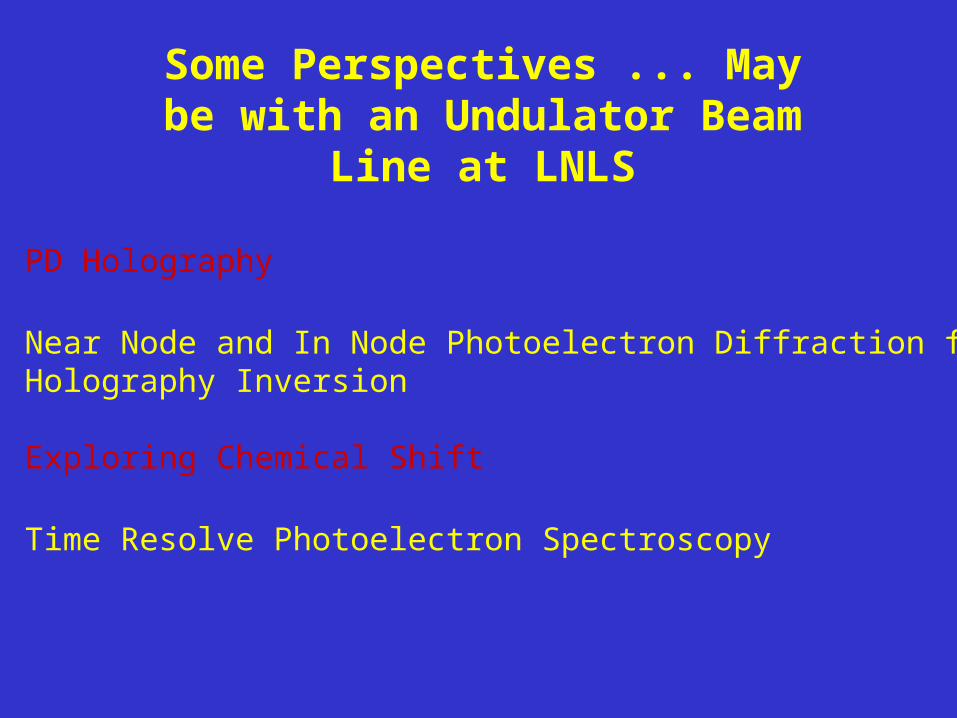
Some Perspectives ... May be with an Undulator Beam
Line at LNLS
• PD Holography
• Near Node and In Node Photoelectron Diffraction for Holography Inversion
• Exploring Chemical Shift
• Time Resolve Photoelectron Spectroscopy


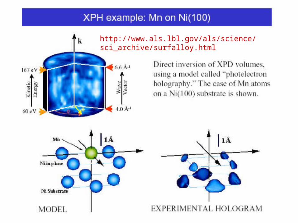
http://www.als.lbl.gov/als/science/sci_archive/surfalloy.html

Colaboradores em PED• Prof. Richard Lander (UNICAMP -SP)
• Prof. George G. Kleiman (UNICAMP-SP)
• Prof. Jonder Morais (UFRGS -RS)
• Prof. Vagner E. De Carvalho (UFMG-MG)
• Prof. Roberto Paniago (UFMG -MG)
• Dr. Edmar A. Soares (UFMG -MG)
• Dr. Carla Bittencourt (UNICAMP -SP)
• PhD. Student Abner de Siervo (UNICAMP-SP)
• Terezinha Ap. Fazan (UNICAMP -SP)
• IUV stuff (LNLS -SP)
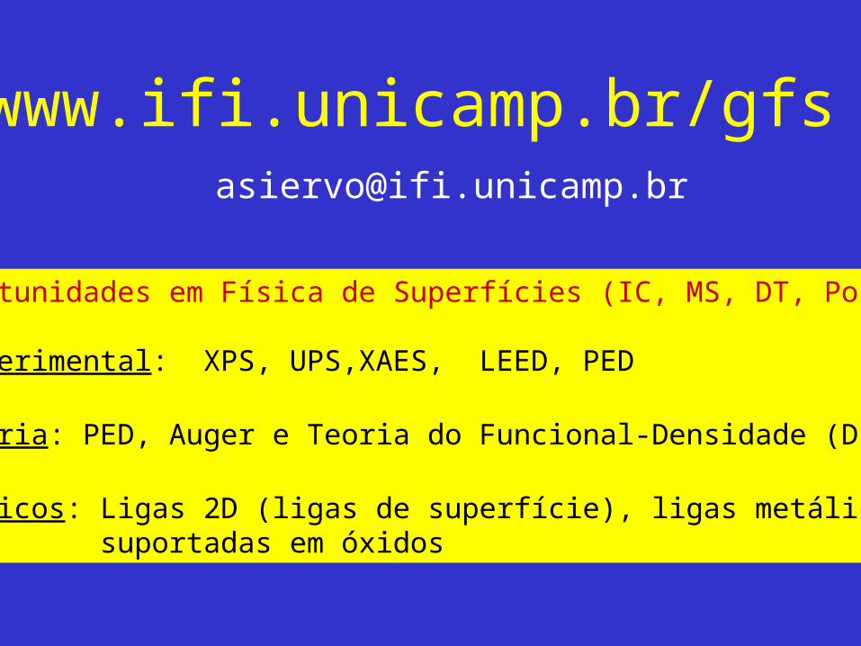
www.ifi.unicamp.br/gfs
Oportunidades em Física de Superfícies (IC, MS, DT, PosDoc)
•Experimental: XPS, UPS,XAES, LEED, PED
•Teoria: PED, Auger e Teoria do Funcional-Densidade (DFT)
•Tópicos: Ligas 2D (ligas de superfície), ligas metálicas suportadas em óxidos

PD Holography for direct 3D atomic images
• Measure I(k) for several k direction and several energies|k|. A volume in k-space can be produce suppression of twin images
~4000 XPS . ( only for high performance beam line !!!)
Szöke (1986), Barton (1988) and several papers Fadley group ( 199x)
• Exploring circular polarized light (CDAD)
•G.H.Fecher, et. al. J.Electron.Spectrosc.Rel. Phen. 76 (1995) 97
• Suppression of forward scattering by“ Near Node photoemission “
^

Advantages of Near Node Photoemission proposed by Osterwalder
From Osterwalder home page

far node near node
Real space
Imaging atom sites with near node photoelectron holographyAl(111) using 2s level p-radiation at the ALOISA beam line - ELETTRA by Osterwalder group.
J. Wider et al., Phys. Rev. Lett. 86, 2337, (2001).

“Near Node” or “In Node” Photoelectron Diffraction at LNLS
* Near Node - Using In-situ omicron AR-65 analyzer : Need New Chamber and twin-plane goniometer
* In Node - Align the backside of Omicron EA 125HR analyzer with SGM beam line . SR traveling through electrostatic lens
In node simulation Near node simulation
Al(111) 2s


![Halliday 4 - Difração (Cap 41 - 4ºed) [HQ]](https://img.document.onl/doc/110x75/5571f84949795991698d110e/halliday-4-difracao-cap-41-4oed-hq.jpg)