Embed Size (px)
Citation preview
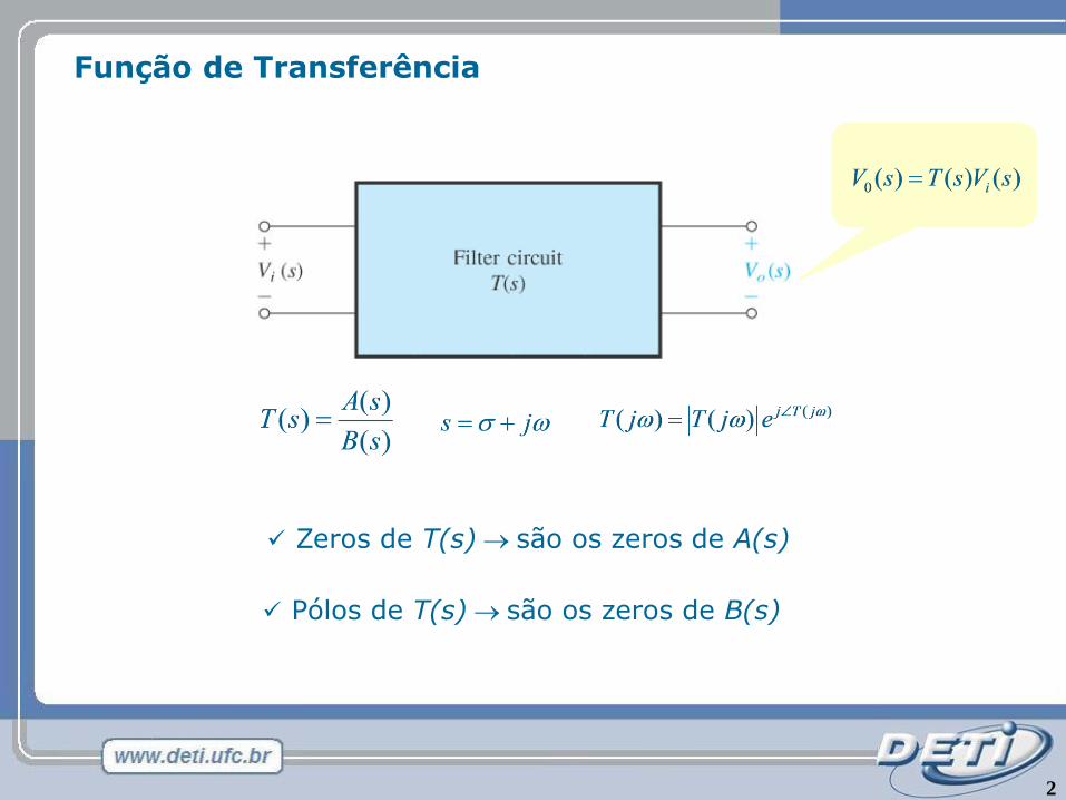
Função de Transferência
Zeros de T(s) são os zeros de A(s)
Pólos de T(s) são os zeros de B(s)
2
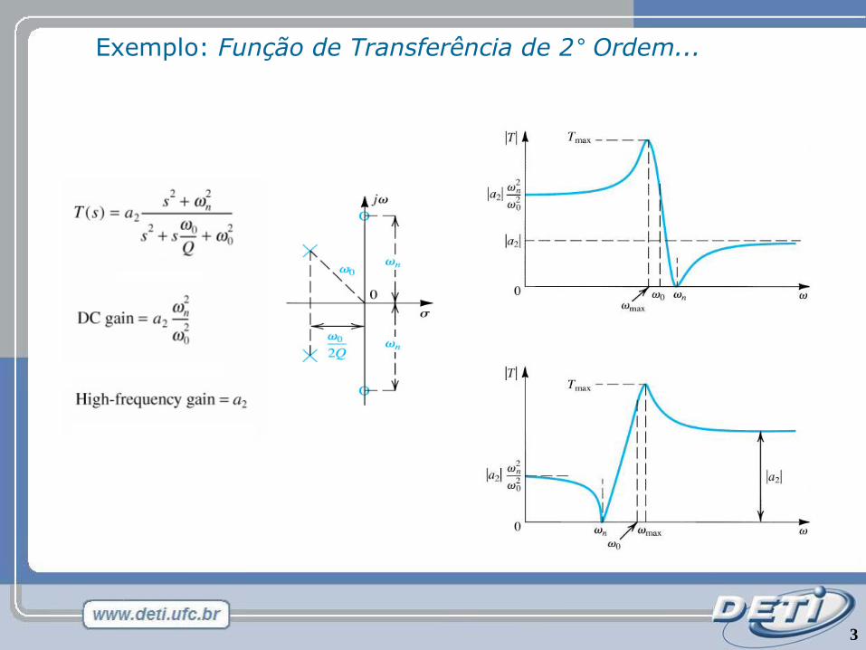
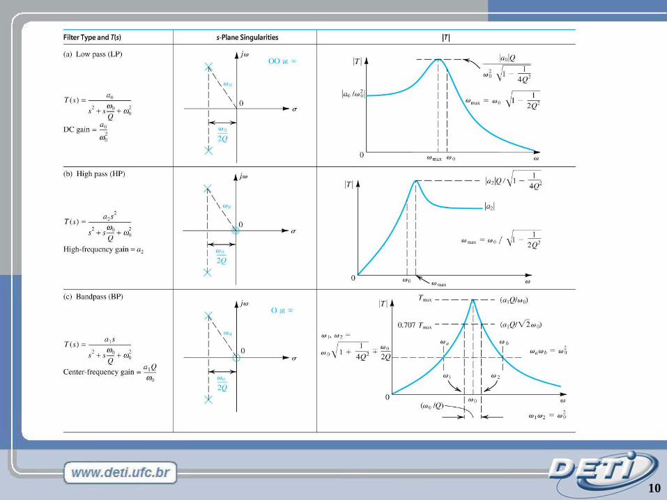
Exemplo: Função de Transferência de 2° Ordem...
3
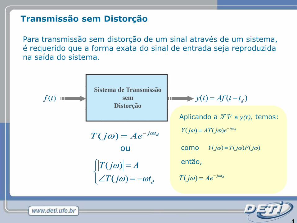
Transmissão sem Distorção
Para transmissão sem distorção de um sinal através de um sistema, é requerido que a forma exata do sinal de entrada seja reproduzida na saída do sistema.
Sistema de Transmissão
sem
Distorção
ou
então,
Aplicando a T F a y(t), temos:
como
4
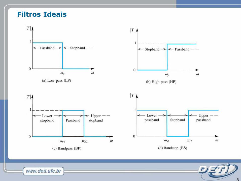
Filtros Ideais
5
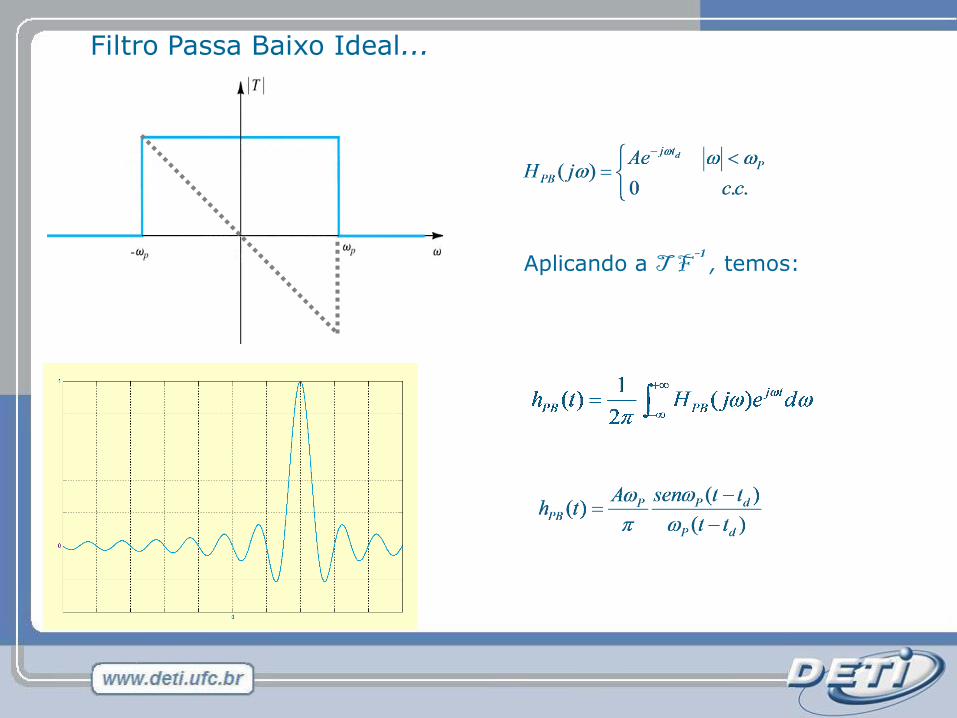
Filtro Passa Baixo Ideal...
Aplicando a T F -1, temos:
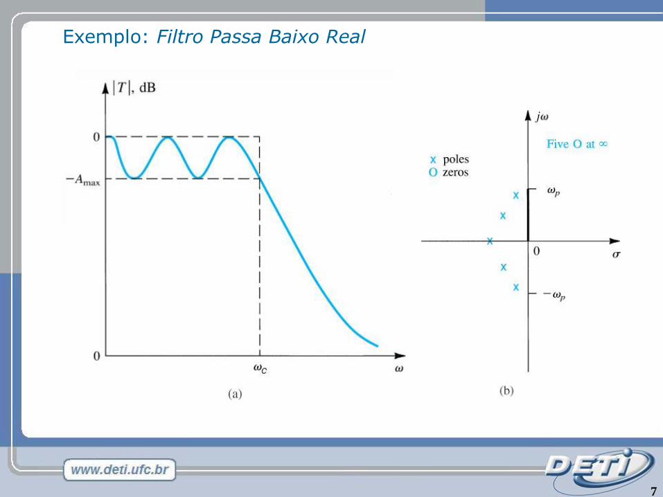
Exemplo: Filtro Passa Baixo Real
7
8
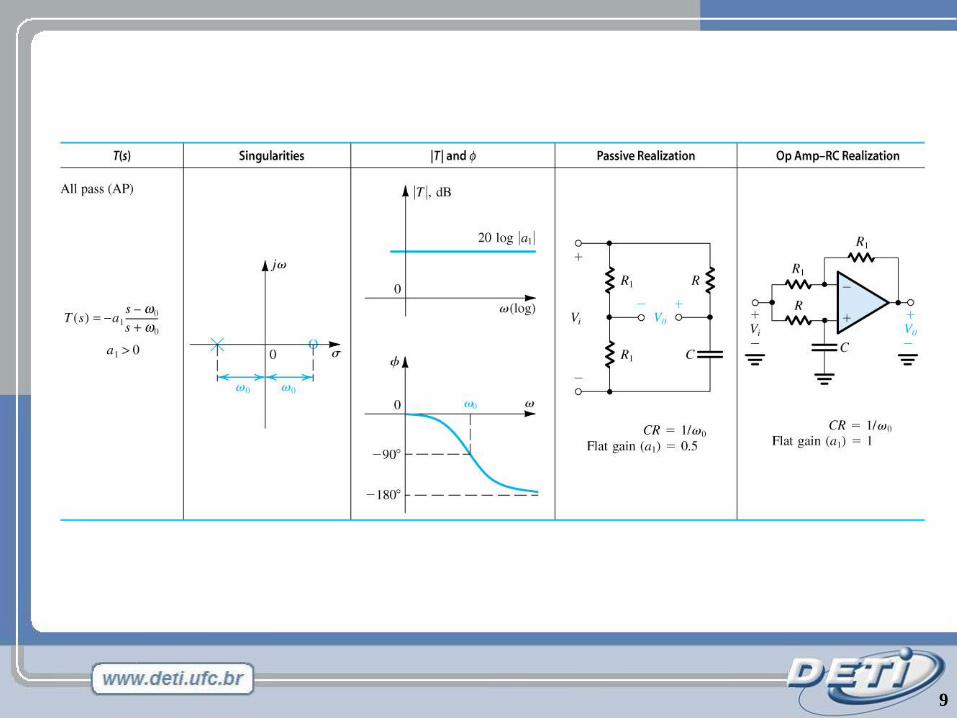
9
10

Especificação de Filtros: Passa Baixo...
11
Modelos de Filtros
Metas ou requerimento para um filtro prático:
Ganho constante na banda passante (r1)
Resposta de fase linear na banda passante (r2)
Máxima rejeição fora da na banda passante (r3)
A simultaneidade destas metas não pode ser alcançada por um único tipo de filtro que seja fisicamente realizável.
Modelos
i. Filtro de Butterworth maximiza a meta (r1)
ii. Filtro de Chebyshev maximiza a meta (r3)
iii. Filtro de Bessel maximiza a meta (r2)
iv. Filtro Elíptico maximiza a meta (r3)
12
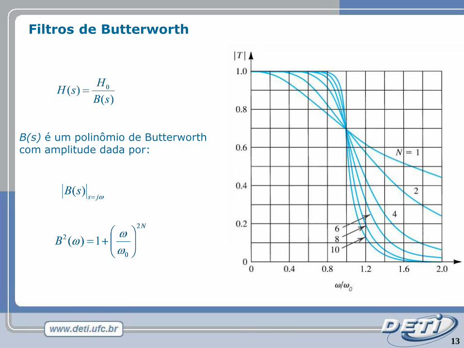
Filtros de Butterworth
B(s) é um polinômio de Butterworth com amplitude dada por:
13
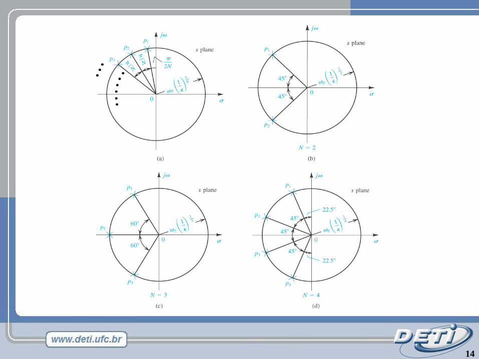
14

(s2 + 0.390s + 1)(s2 + 1.111s + 1)(s2 + 1.663s + 1)(s2 + 1.962s + 1)8
(s + 1)(s2 + 0.445s + 1)(s2 + 1.247s + 1)(s2 + 1.802s + 1)7
(s2 + 0.518s + 1)(s2 + 1.414s + 1)(s2 + 1.932s + 1)6
(s + 1)(s2 + 0.618s + 1)(s2 + 1.618s + 1)5
(s2 + 0.765s + 1)(s2 + 1.848s + 1)4
(s+1)(s2 + s + 1)3
s2 + 1.414s + 12
s +11
Fatores de Polinômios BN(s) NormalizadosN
15
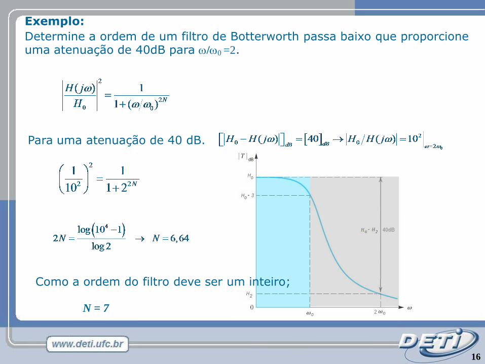
Exemplo:
Determine a ordem de um filtro de Botterworth passa baixo que proporcione uma atenuação de 40dB para /0 =2.
Para uma atenuação de 40 dB.
Como a ordem do filtro deve ser um inteiro;
N = 7
16
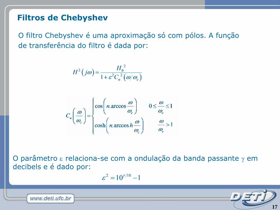
Filtros de Chebyshev
O filtro Chebyshev é uma aproximação só com pólos. A função
de transferência do filtro é dada por:
O parâmetro relaciona-se com a ondulação da banda passante em decibels e é dado por:
17
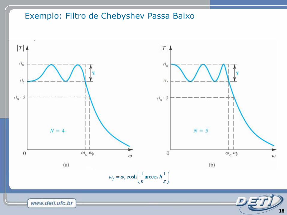
Exemplo: Filtro de Chebyshev Passa Baixo
18
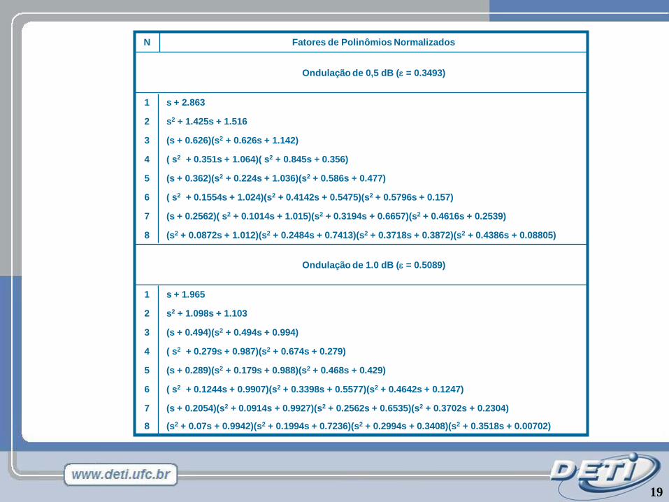
(s2 + 0.07s + 0.9942)(s2 + 0.1994s + 0.7236)(s2 + 0.2994s + 0.3408)(s2 + 0.3518s + 0.00702)8
(s + 0.2054)(s2 + 0.0914s + 0.9927)(s2 + 0.2562s + 0.6535)(s2 + 0.3702s + 0.2304)7
( s2 + 0.1244s + 0.9907)(s2 + 0.3398s + 0.5577)(s2 + 0.4642s + 0.1247)6
(s + 0.289)(s2 + 0.179s + 0.988)(s2 + 0.468s + 0.429)5
( s2 + 0.279s + 0.987)(s2 + 0.674s + 0.279)4
(s + 0.494)(s2 + 0.494s + 0.994)3
s2 + 1.098s + 1.1032
s + 1.9651
Ondulação de 1.0 dB ( = 0.5089)
(s2 + 0.0872s + 1.012)(s2 + 0.2484s + 0.7413)(s2 + 0.3718s + 0.3872)(s2 + 0.4386s + 0.08805)8
(s + 0.2562)( s2 + 0.1014s + 1.015)(s2 + 0.3194s + 0.6657)(s2 + 0.4616s + 0.2539)7
( s2 + 0.1554s + 1.024)(s2 + 0.4142s + 0.5475)(s2 + 0.5796s + 0.157)6
(s + 0.362)(s2 + 0.224s + 1.036)(s2 + 0.586s + 0.477)5
( s2 + 0.351s + 1.064)( s2 + 0.845s + 0.356)4
(s + 0.626)(s2 + 0.626s + 1.142)3
s2 + 1.425s + 1.5162
s + 2.8631
Ondulação de 0,5 dB ( = 0.3493)
Fatores de Polinômios Normalizados N
19
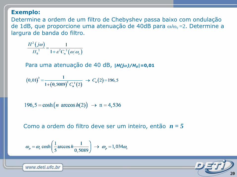
Exemplo:
Determine a ordem de um filtro de Chebyshev passa baixo com ondulação de 1dB, que proporcione uma atenuação de 40dB para /c =2. Determine a
largura de banda do filtro.
Para uma atenuação de 40 dB, |H(j)/H0|=0,01
Como a ordem do filtro deve ser um inteiro, então n = 5
20
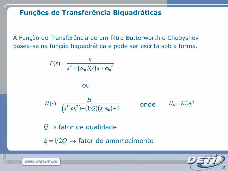
Funções de Transferência Biquadráticas
A Função de Transferência de um filtro Butterworth e Chebyshev
basea-se na função biquadrática e pode ser escrita sob a forma.
ou
onde
fator de amortecimento
fator de qualidade
21
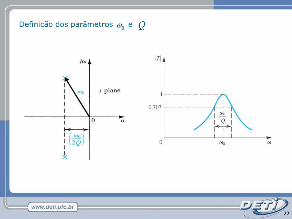
Definição dos parâmetros e
22
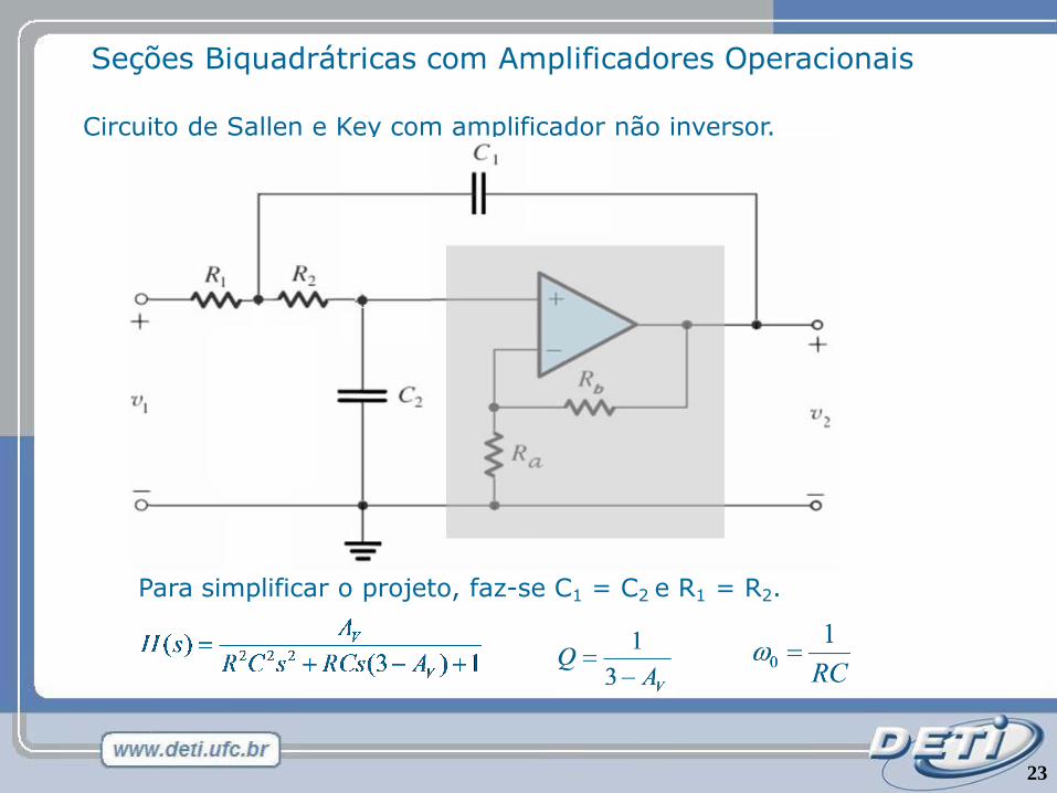
Seções Biquadrátricas com Amplificadores Operacionais
Circuito de Sallen e Key com amplificador não inversor.
Para simplificar o projeto, faz-se C1 = C2 e R1 = R2.
23
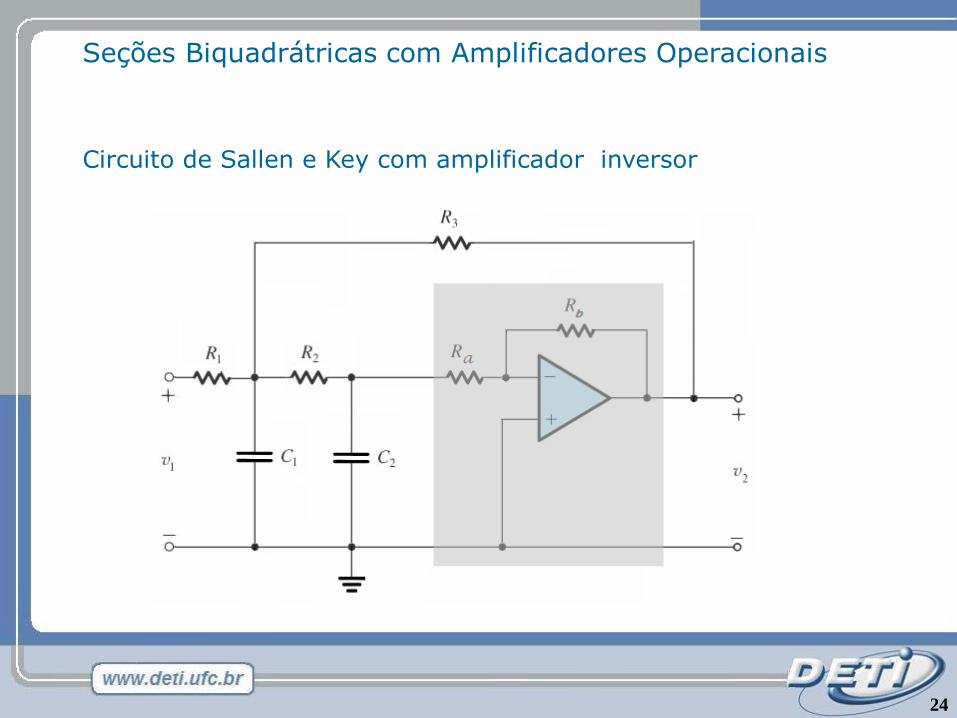
Seções Biquadrátricas com Amplificadores Operacionais
Circuito de Sallen e Key com amplificador inversor
24
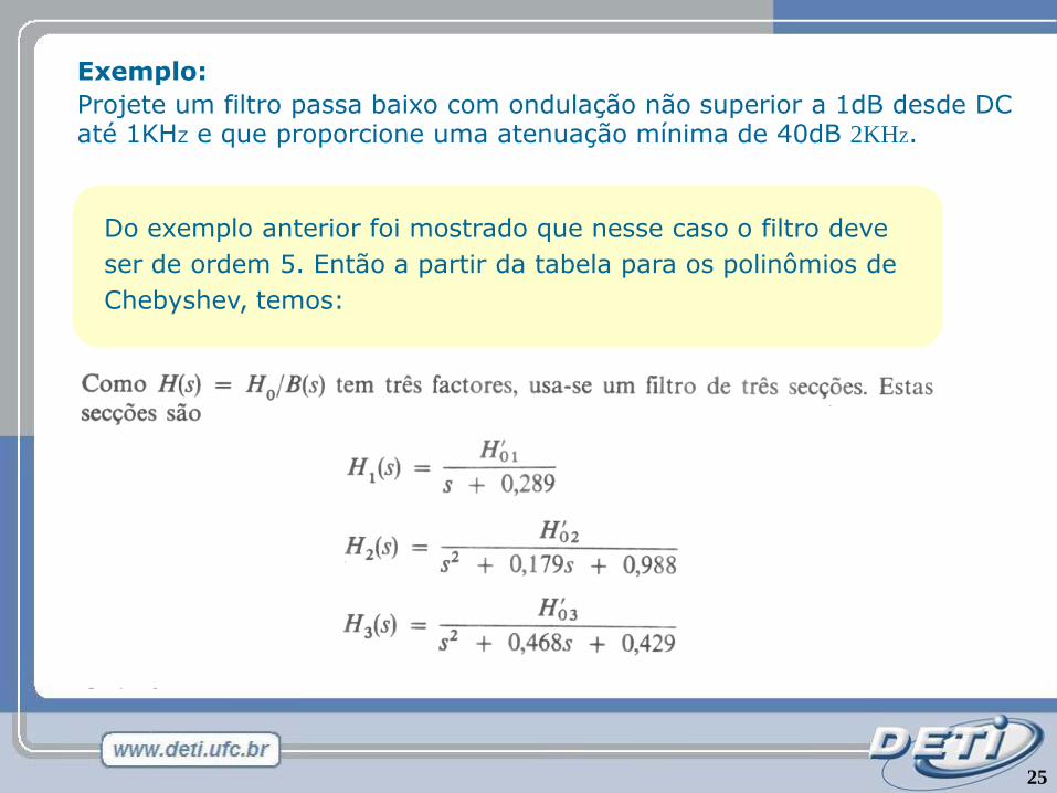
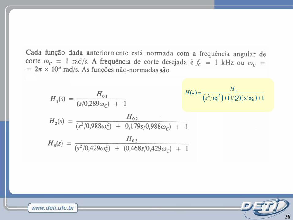
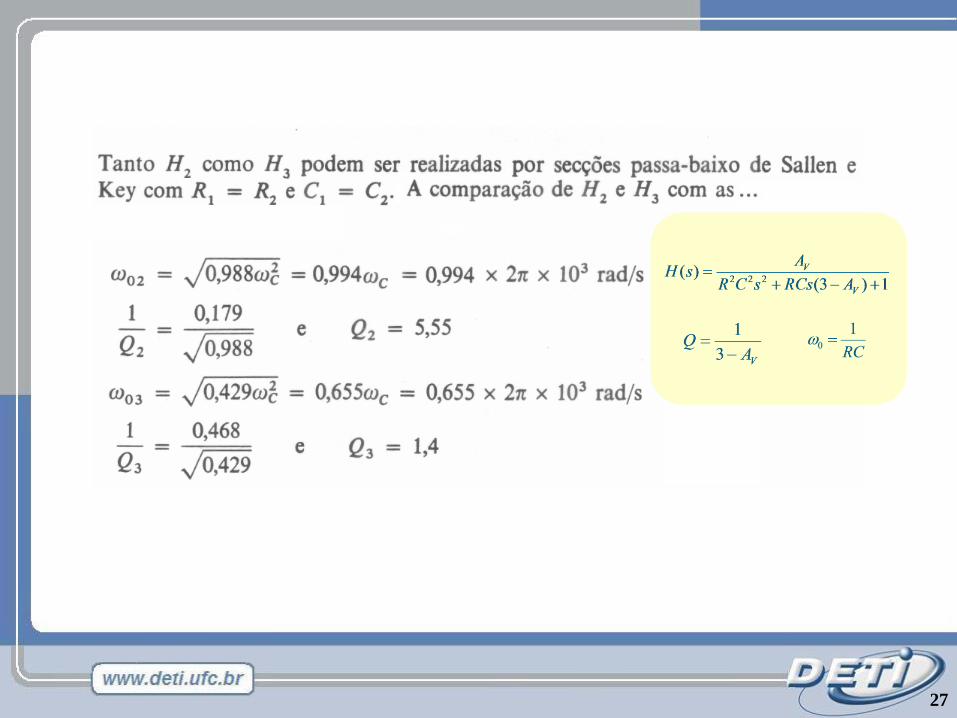
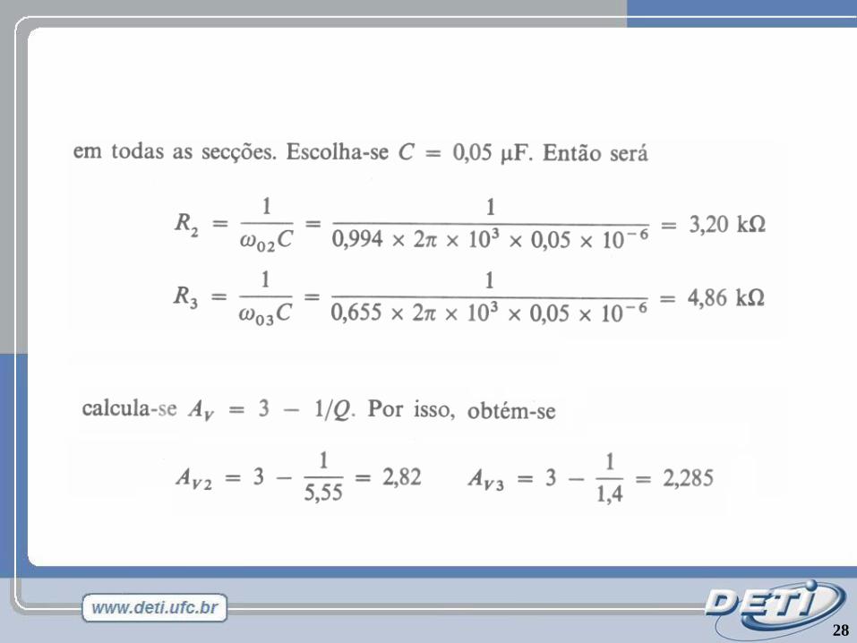
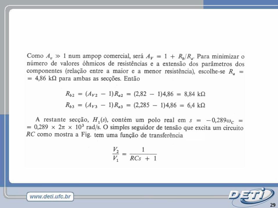
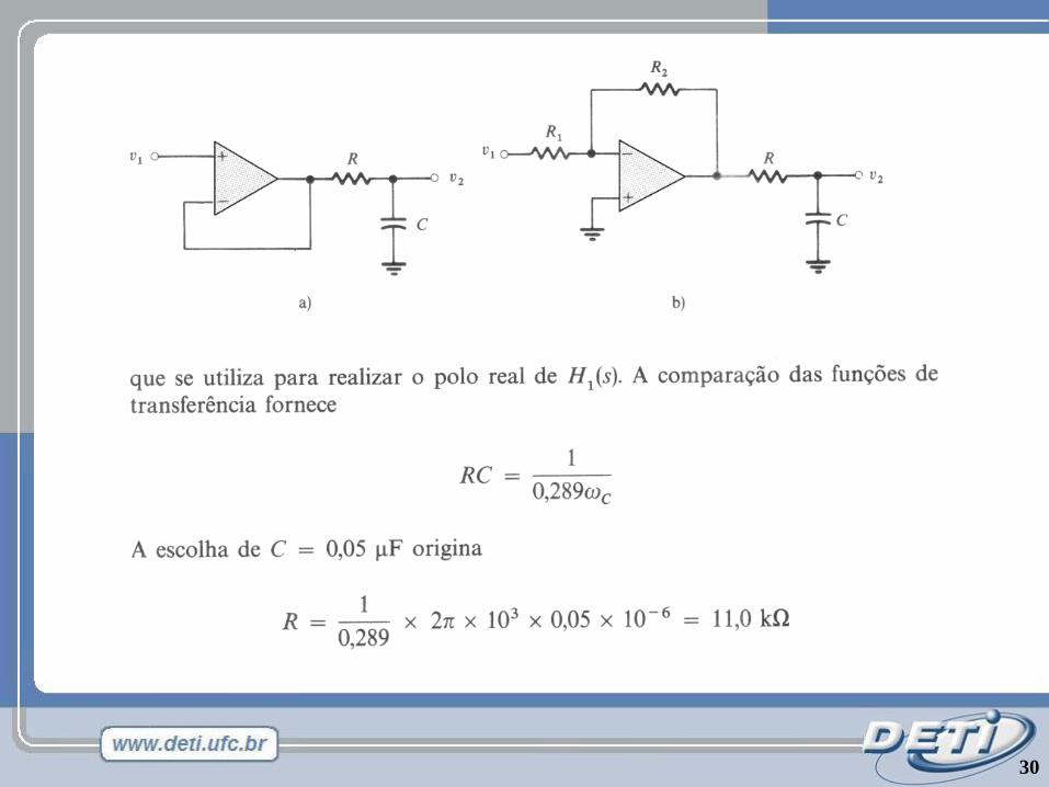
Exemplo:
Projete um filtro passa baixo com ondulação não superior a 1dB desde DC até 1KHZ e que proporcione uma atenuação mínima de 40dB 2KHZ.
Do exemplo anterior foi mostrado que nesse caso o filtro deve
ser de ordem 5. Então a partir da tabela para os polinômios de
Chebyshev, temos:
25
26
27
28
29
30
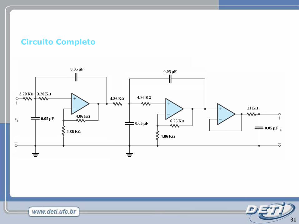
3.20 KΩ 3.20 KΩ
4.86 KΩ
4.86 KΩ
4.86 KΩ 4.86 KΩ
4.86 KΩ
6.25 KΩ
11 KΩ
0.05 µF
0.05 µF0.05 µF
0.05 µF0.05 µF
Circuito Completo
31
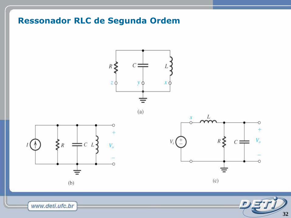
Ressonador RLC de Segunda Ordem
32
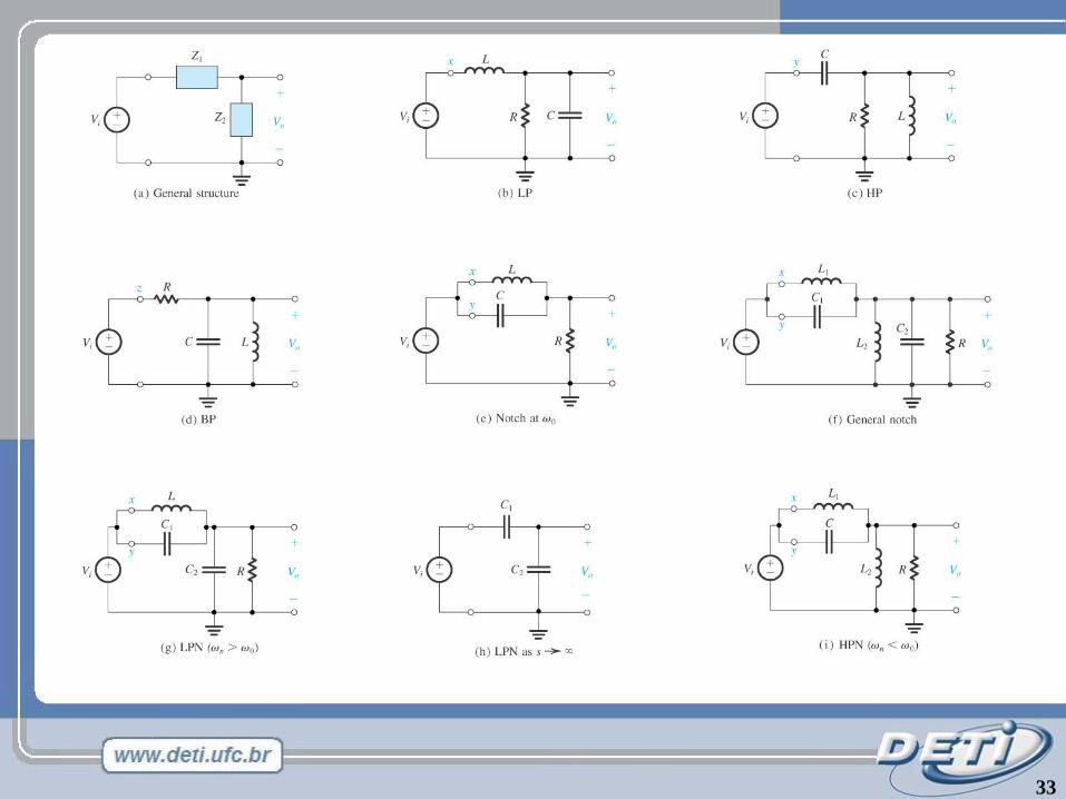
33
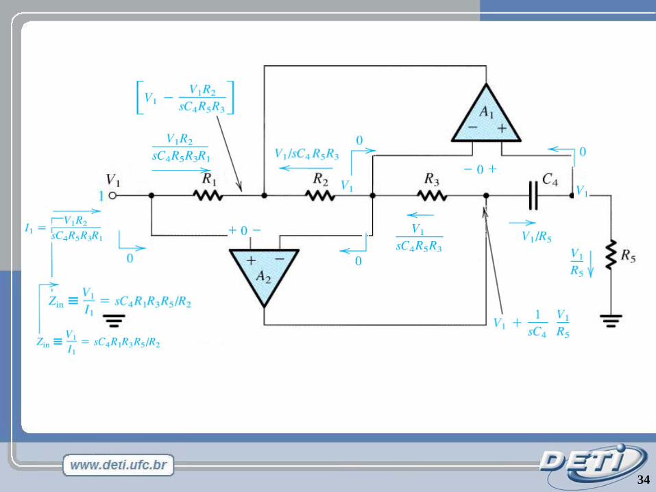
34
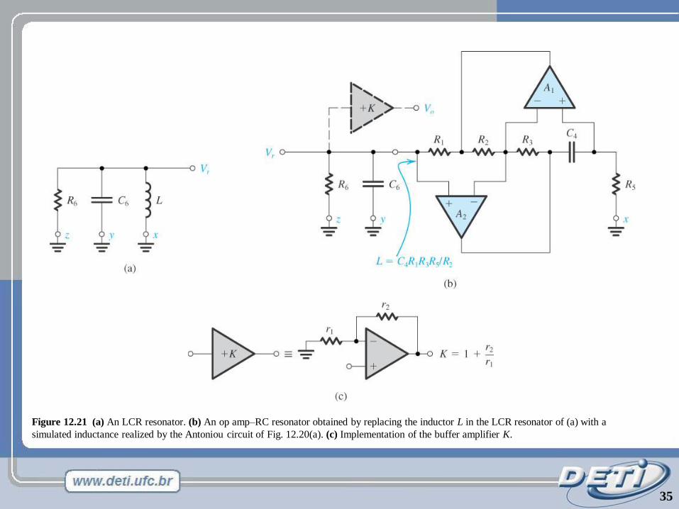
Figure 12.21 (a) An LCR resonator. (b) An op amp–RC resonator obtained by replacing the inductor L in the LCR resonator of (a) with a
simulated inductance realized by the Antoniou circuit of Fig. 12.20(a). (c) Implementation of the buffer amplifier K.
35
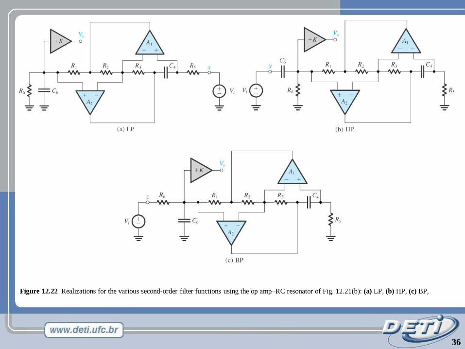
Figure 12.22 Realizations for the various second-order filter functions using the op amp–RC resonator of Fig. 12.21(b): (a) LP, (b) HP, (c) BP,
36
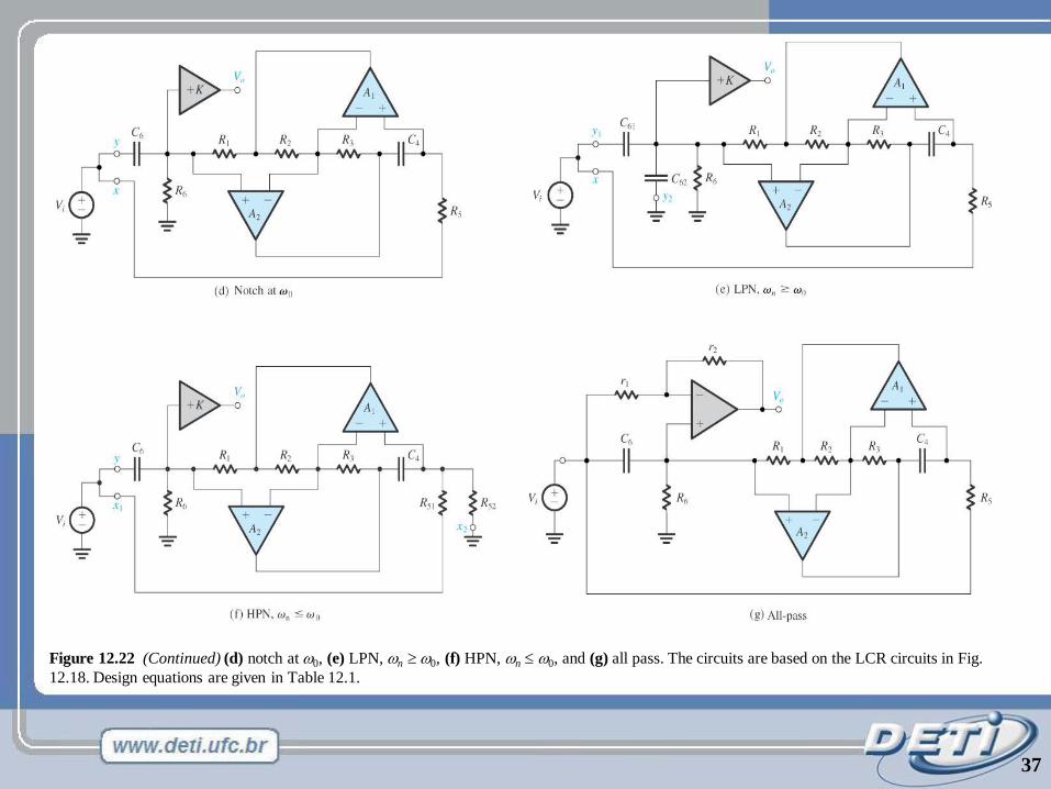
Figure 12.22 (Continued) (d) notch at 0, (e) LPN, n 0, (f) HPN, n 0, and (g) all pass. The circuits are based on the LCR circuits in Fig.
12.18. Design equations are given in Table 12.1.
37
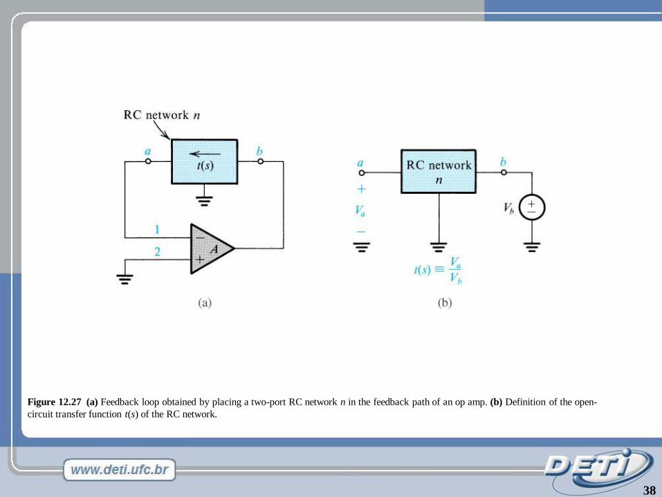
Figure 12.27 (a) Feedback loop obtained by placing a two-port RC network n in the feedback path of an op amp. (b) Definition of the open-
circuit transfer function t(s) of the RC network.
38
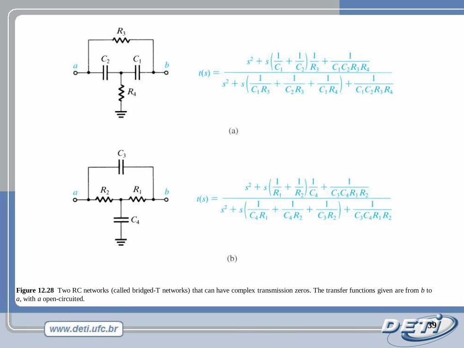
Figure 12.28 Two RC networks (called bridged-T networks) that can have complex transmission zeros. The transfer functions given are from b to
a, with a open-circuited.
39
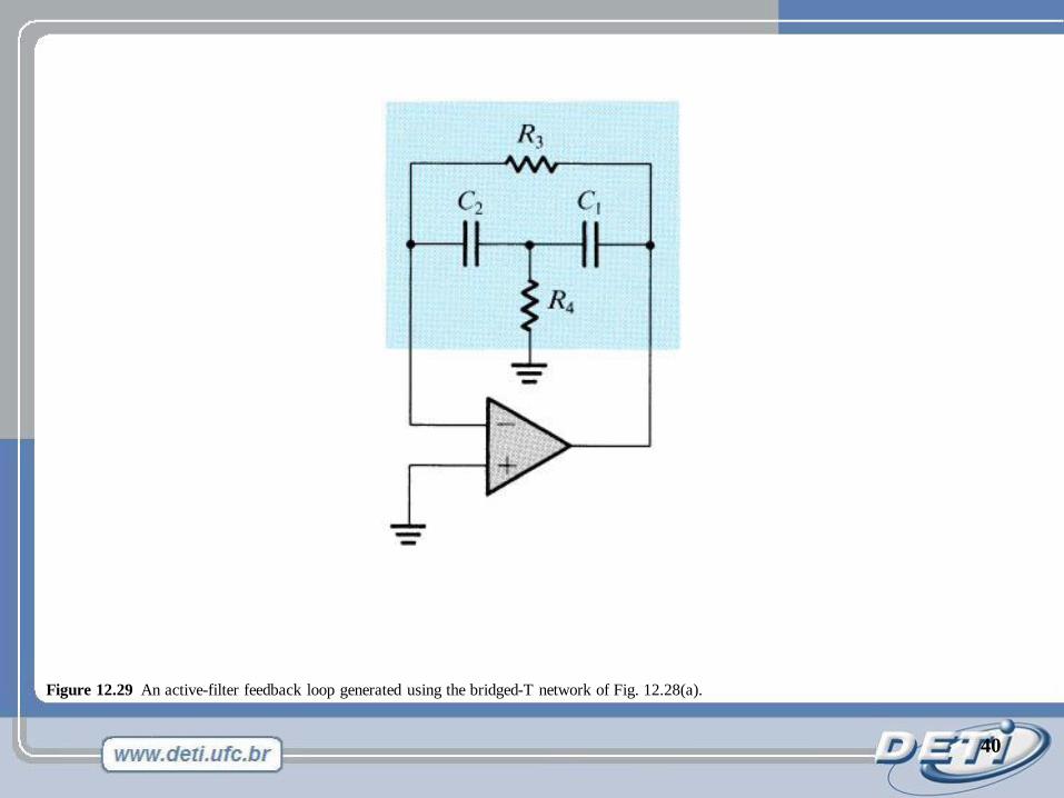
Figure 12.29 An active-filter feedback loop generated using the bridged-T network of Fig. 12.28(a).
40
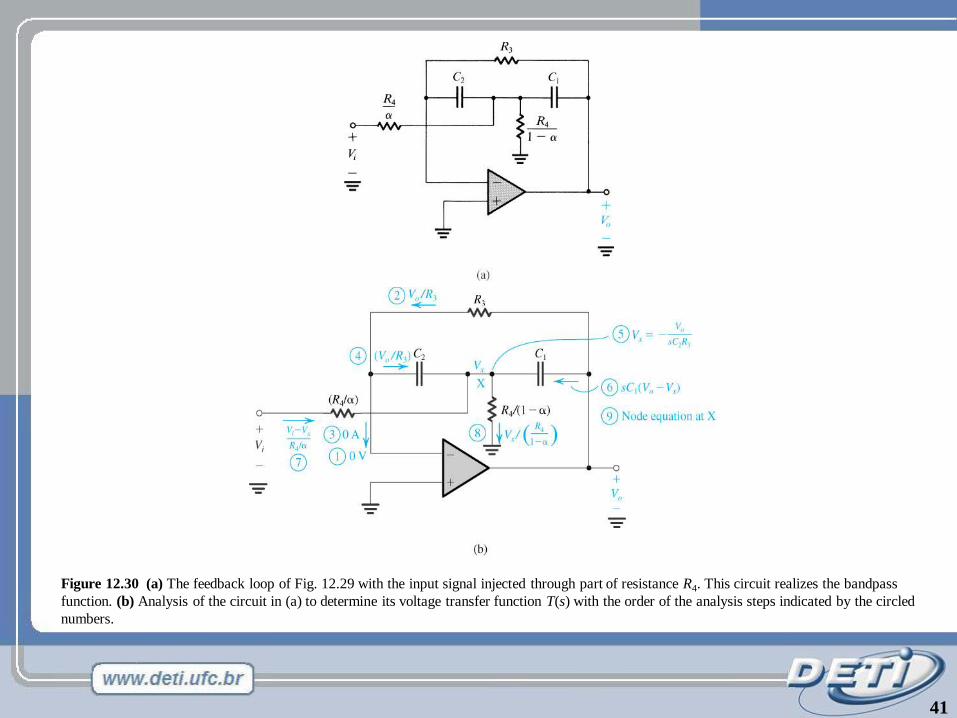
Figure 12.30 (a) The feedback loop of Fig. 12.29 with the input signal injected through part of resistance R4. This circuit realizes the bandpass
function. (b) Analysis of the circuit in (a) to determine its voltage transfer function T(s) with the order of the analysis steps indicated by the circled
numbers.
41
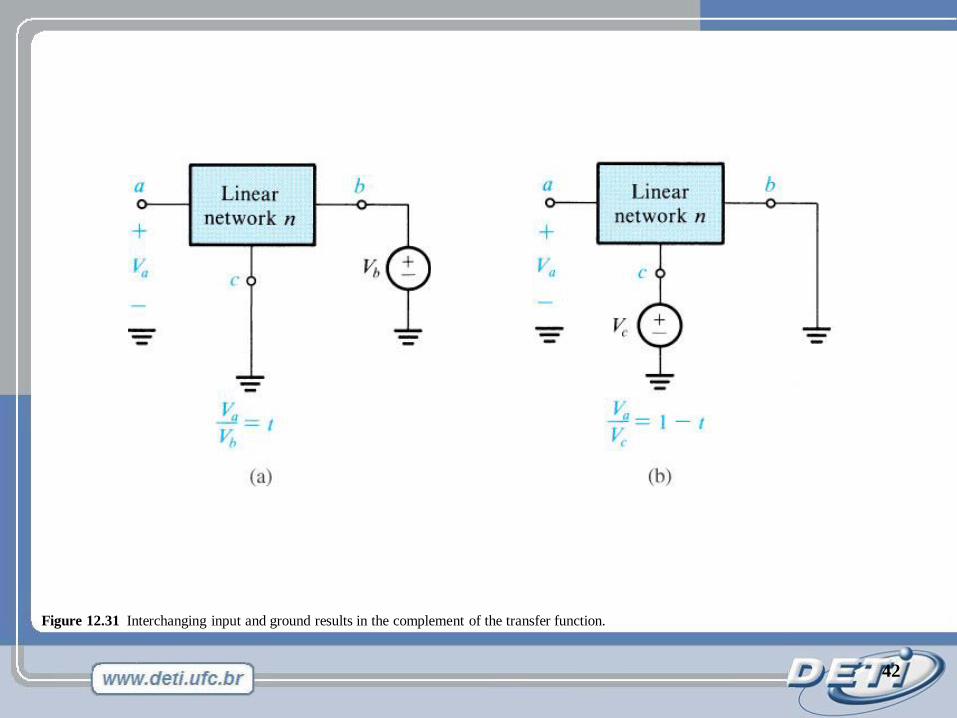
Figure 12.31 Interchanging input and ground results in the complement of the transfer function.
42
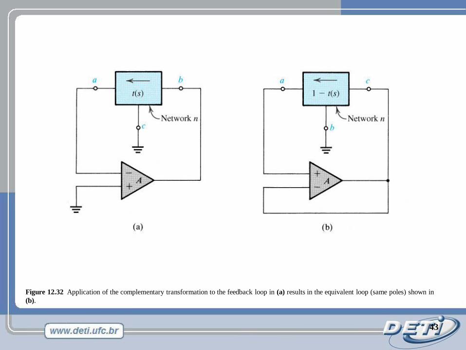
Figure 12.32 Application of the complementary transformation to the feedback loop in (a) results in the equivalent loop (same poles) shown in
(b).
43
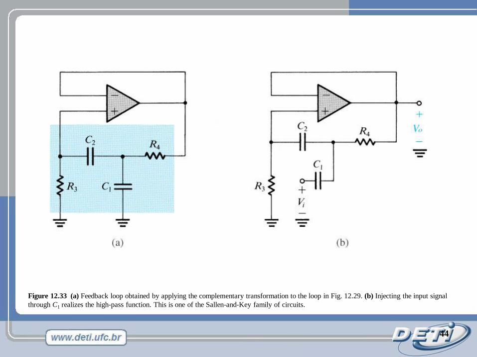
Figure 12.33 (a) Feedback loop obtained by applying the complementary transformation to the loop in Fig. 12.29. (b) Injecting the input signal
through C1 realizes the high-pass function. This is one of the Sallen-and-Key family of circuits.
44
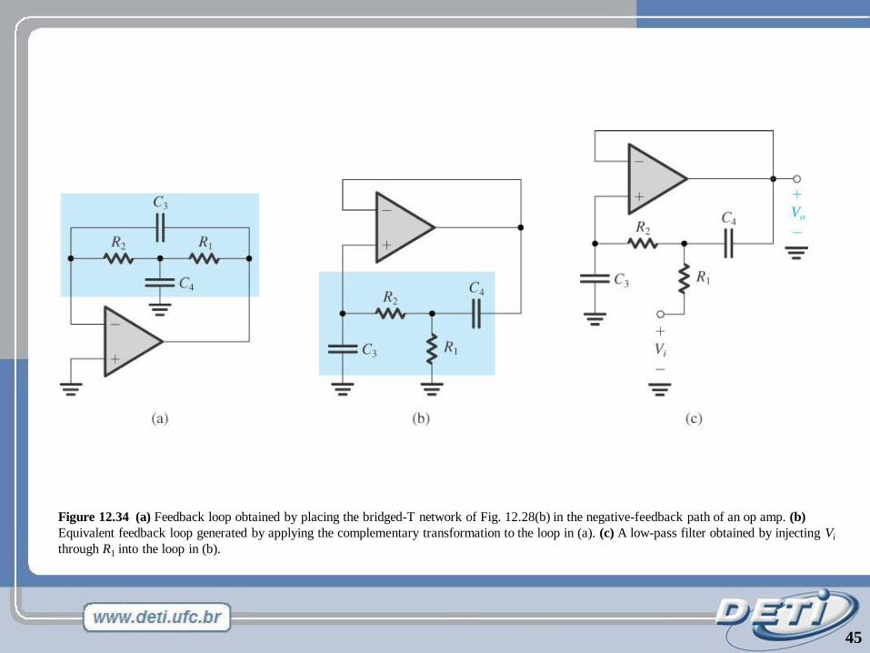
Figure 12.34 (a) Feedback loop obtained by placing the bridged-T network of Fig. 12.28(b) in the negative-feedback path of an op amp. (b)
Equivalent feedback loop generated by applying the complementary transformation to the loop in (a). (c) A low-pass filter obtained by injecting Vi
through R1 into the loop in (b).
45
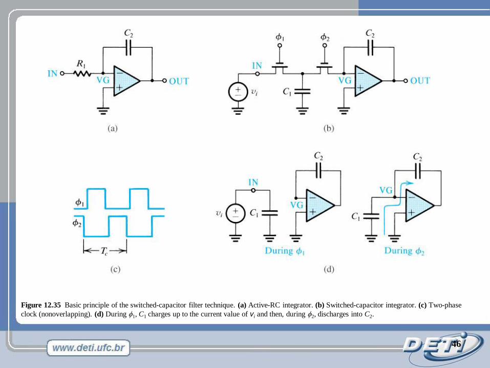
Figure 12.35 Basic principle of the switched-capacitor filter technique. (a) Active-RC integrator. (b) Switched-capacitor integrator. (c) Two-phase
clock (nonoverlapping). (d) During f1, C1 charges up to the current value of vi and then, during f2, discharges into C2.
46
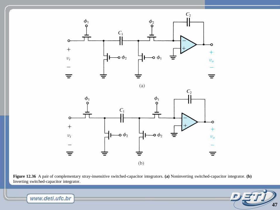
Figure 12.36 A pair of complementary stray-insensitive switched-capacitor integrators. (a) Noninverting switched-capacitor integrator. (b)
Inverting switched-capacitor integrator.
47
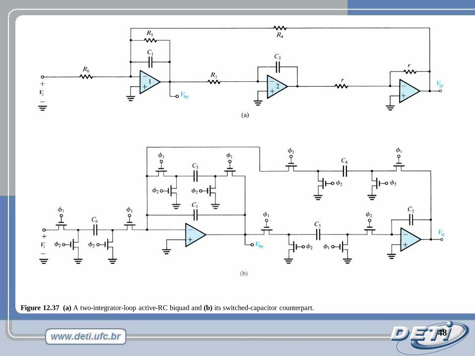
Figure 12.37 (a) A two-integrator-loop active-RC biquad and (b) its switched-capacitor counterpart.
48
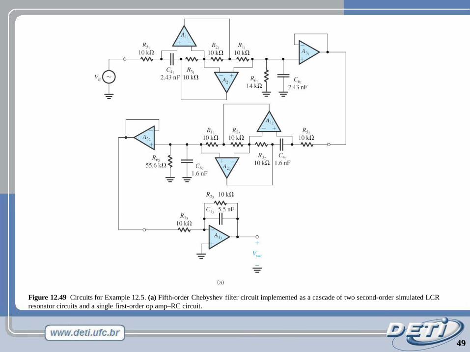
Figure 12.49 Circuits for Example 12.5. (a) Fifth-order Chebyshev filter circuit implemented as a cascade of two second-order simulated LCR
resonator circuits and a single first-order op amp–RC circuit.
49
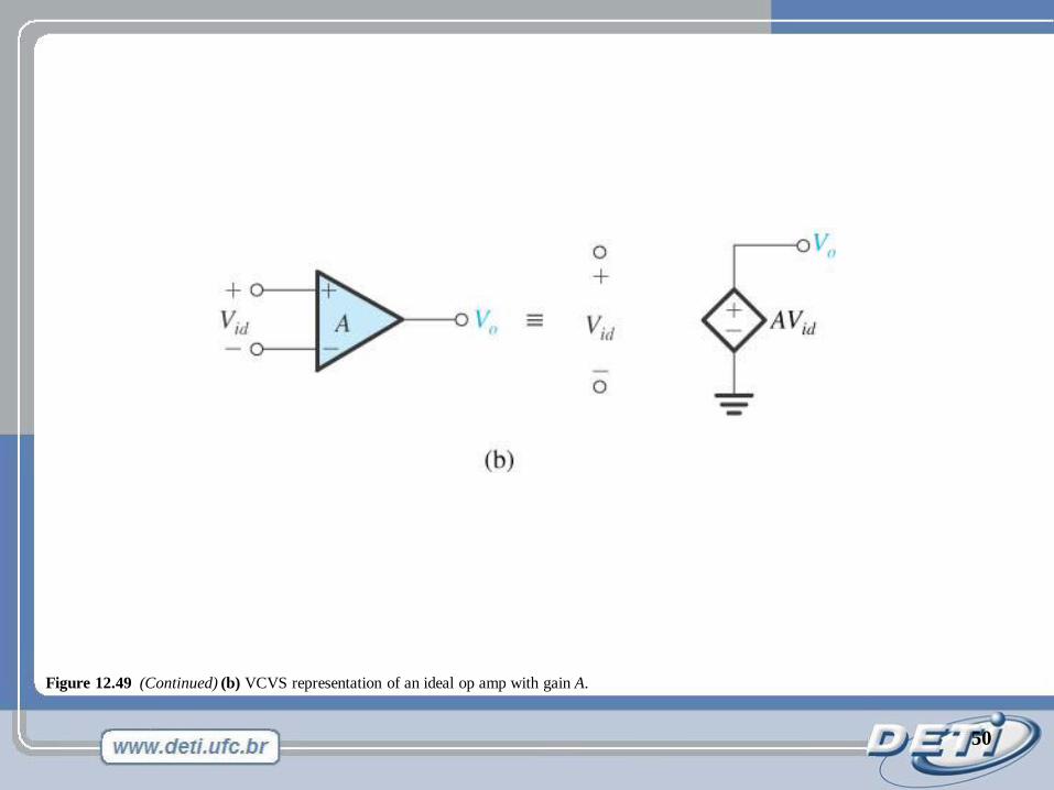
Figure 12.49 (Continued) (b) VCVS representation of an ideal op amp with gain A.
50
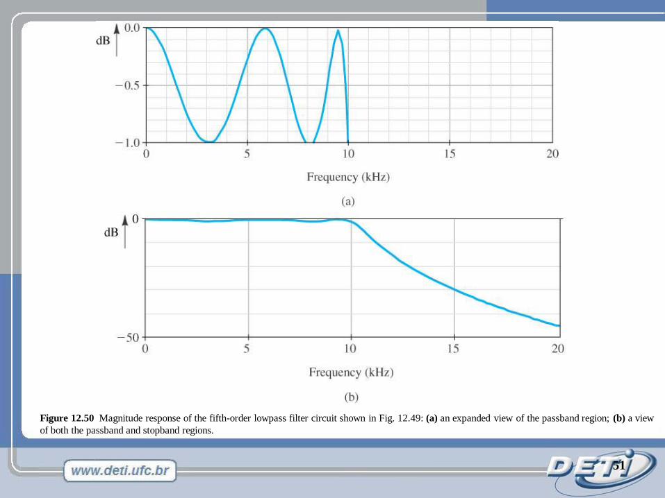
Figure 12.50 Magnitude response of the fifth-order lowpass filter circuit shown in Fig. 12.49: (a) an expanded view of the passband region; (b) a view
of both the passband and stopband regions.
51
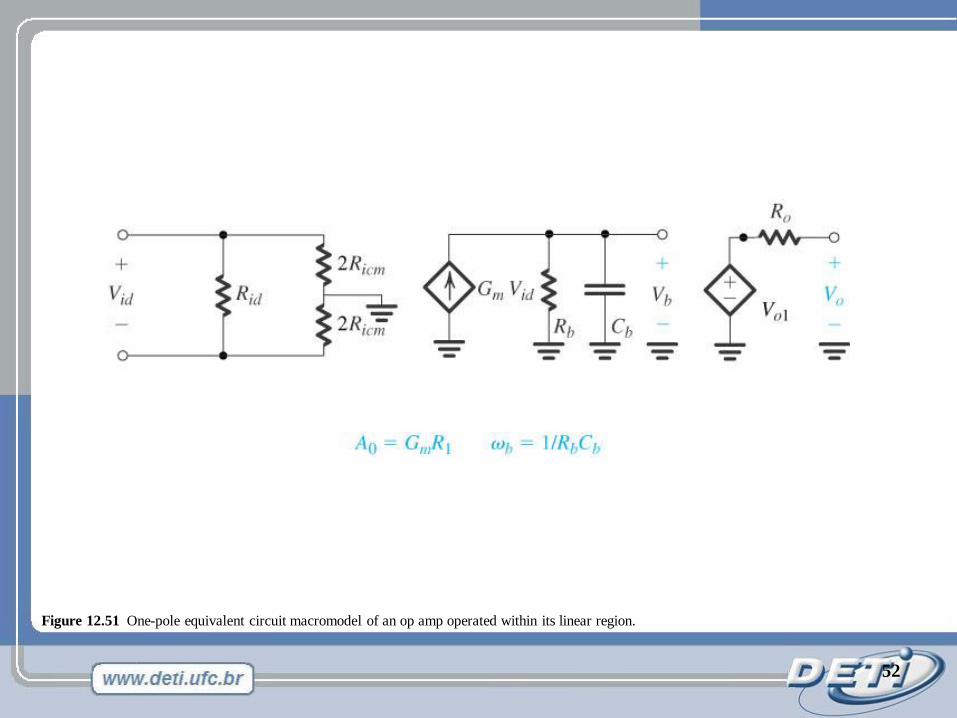
Figure 12.51 One-pole equivalent circuit macromodel of an op amp operated within its linear region.
52
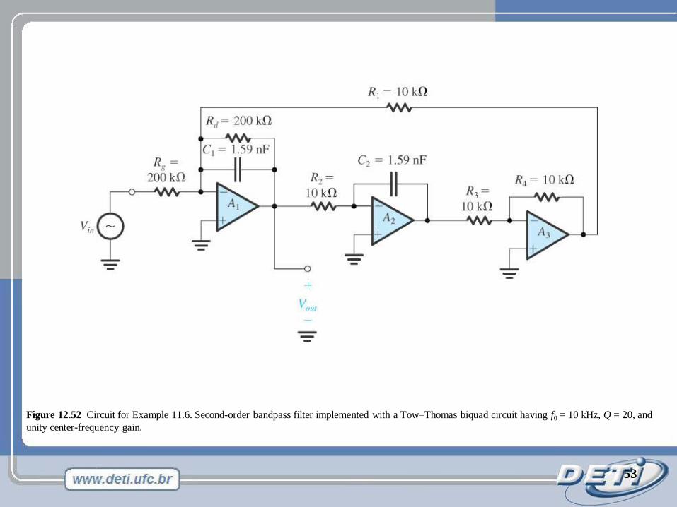
Figure 12.52 Circuit for Example 11.6. Second-order bandpass filter implemented with a Tow–Thomas biquad circuit having f0 = 10 kHz, Q = 20, and
unity center-frequency gain.
53
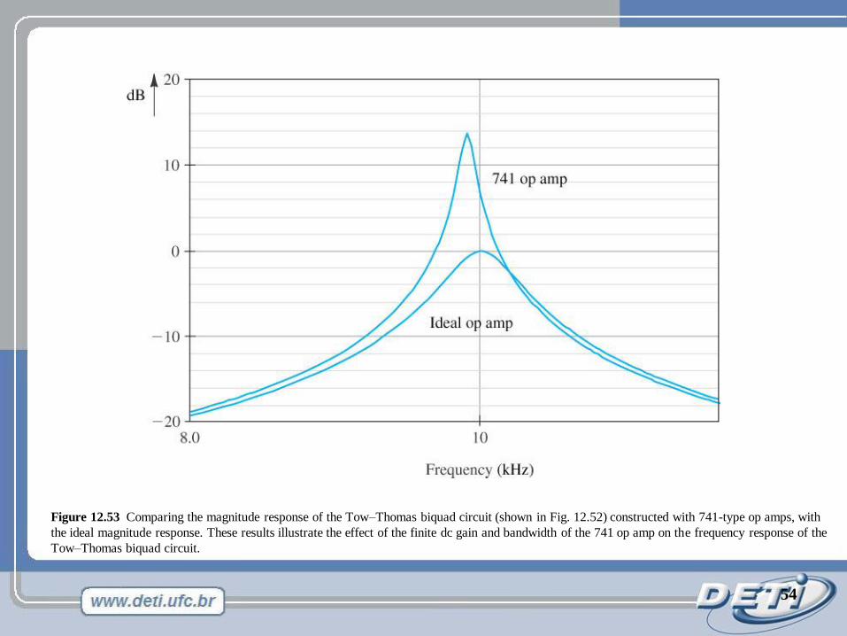
Figure 12.53 Comparing the magnitude response of the Tow–Thomas biquad circuit (shown in Fig. 12.52) constructed with 741-type op amps, with
the ideal magnitude response. These results illustrate the effect of the finite dc gain and bandwidth of the 741 op amp on the frequency response of the
Tow–Thomas biquad circuit.
54
Figure 12.54 (a) Magnitude response of the Tow–Thomas biquad circuit with different values of compensation capacitance. For comparison, the ideal
response is also shown.
55
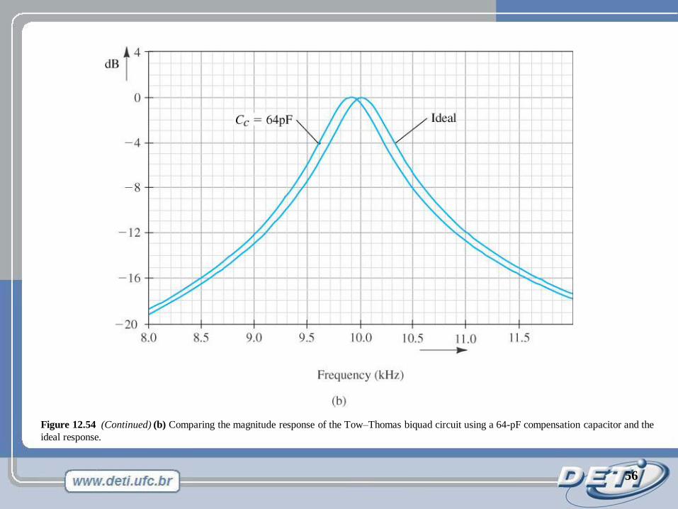
Figure 12.54 (Continued) (b) Comparing the magnitude response of the Tow–Thomas biquad circuit using a 64-pF compensation capacitor and the
ideal response.
56