Embed Size (px)
Citation preview
Aula
Disciplina: Sistemas Digitais – Profa. Dra. Fernanda Gusmão de Lima Kastensmidt – 20061 / 30
Introdução a Sistemas DigitaisIntrodução a Sistemas Digitais
Uso de banco de registradores e Memorias
Aula
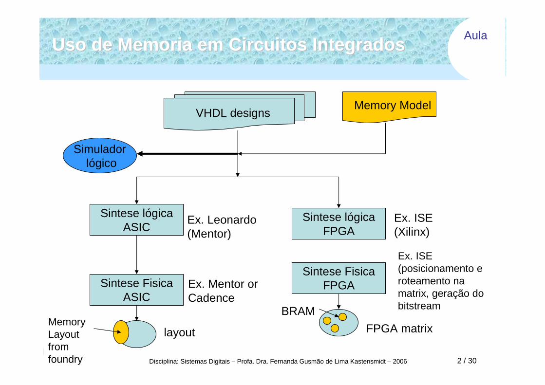
Disciplina: Sistemas Digitais – Profa. Dra. Fernanda Gusmão de Lima Kastensmidt – 2006 2 / 30
UsoUso de de MemoriaMemoria emem CircuitosCircuitos IntegradosIntegrados
VHDL designs
Sintese lógicaASIC
Sintese lógicaFPGA
Ex. Leonardo(Mentor)
Ex. ISE(Xilinx)
Ex. Mentor or Cadence
Sintese FisicaASIC
Sintese FisicaFPGA
Ex. ISE (posicionamento e roteamento namatrix, geração do bitstream
Memory Model
layout FPGA matrixBRAM
MemoryLayout from foundry
Simuladorlógico
Aula
Disciplina: Sistemas Digitais – Profa. Dra. Fernanda Gusmão de Lima Kastensmidt – 2006 3 / 30
Leitura e Escrita em MemoriaLeitura e Escrita em Memoria
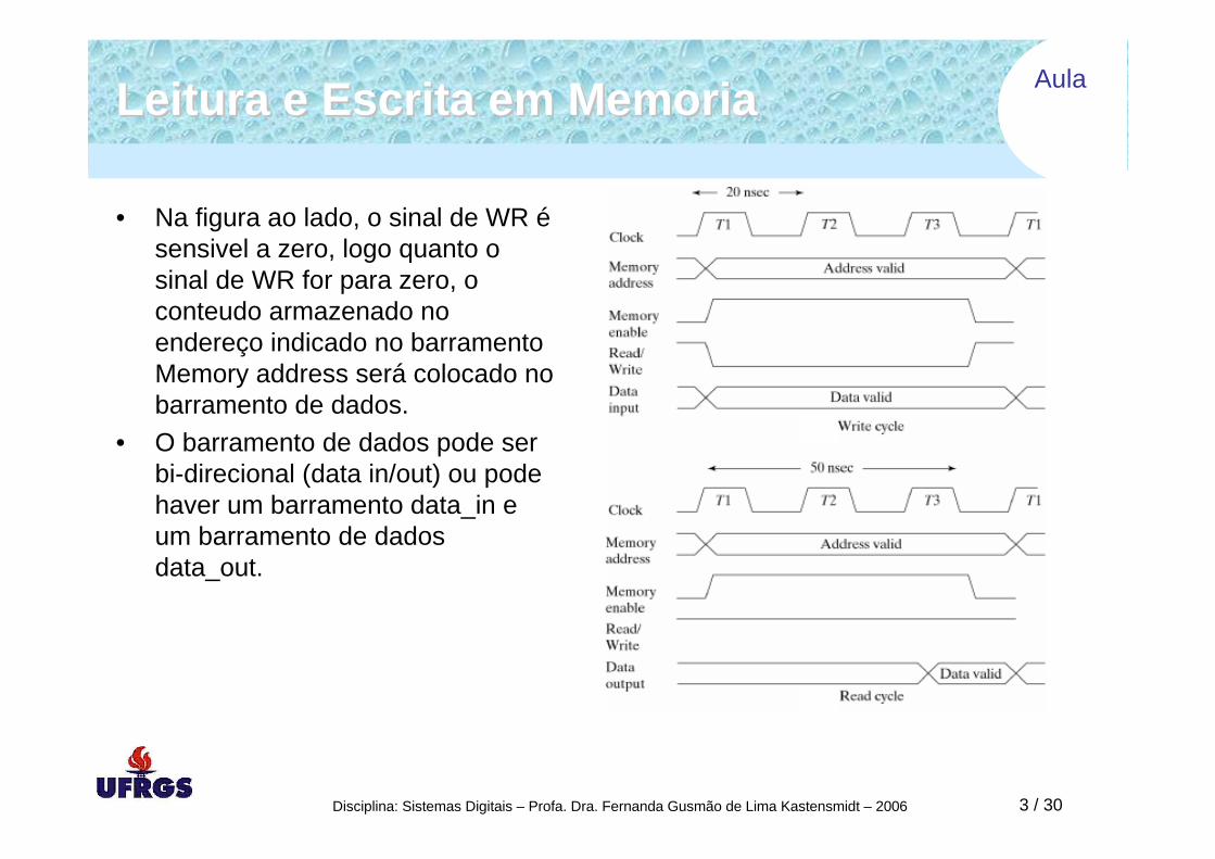
• Na figura ao lado, o sinal de WR é sensivel a zero, logo quanto o sinal de WR for para zero, o conteudo armazenado no endereço indicado no barramentoMemory address será colocado no barramento de dados.
• O barramento de dados pode ser bi-direcional (data in/out) ou podehaver um barramento data_in e um barramento de dados data_out.

Aula
Disciplina: Sistemas Digitais – Profa. Dra. Fernanda Gusmão de Lima Kastensmidt – 2006 4 / 30
Descrição de Memoria em VHDLDescrição de Memoria em VHDLlibrary IEEE;use IEEE.std_logic_1164.all;library BITLIB;use BITLIB.bit_pack.all;
entity RAM6116 isport(Cs_b, We_b: in bit;Address: in bit_vector(7 downto 0);IO: inout std_logic_vector(7 downto 0));end RAM6116;
architecture simple_ram of RAM6116 is
type RAMtype is array(0 to 255) of std_logic_vector(7 downto 0);signal RAM1: RAMtype:=(others=> (others=>'0')); -- Initialize all bits to '0‘
Begin
processbeginif Cs_b = '1' then IO <= "ZZZZZZZZ"; -- chip not selectedelseif We_b'event and We_b = '1' then -- rising-edge of We_bRAM1(vec2int(Address'delayed)) <= IO; -- writewait for 0 ns; -- wait for RAM updateend if;if We_b = '1' thenIO <= RAM1(vec2int(Address)); -- readelse IO <= "ZZZZZZZZ"; -- drive high-Zend if;end if;wait on We_b, Cs_b, Address;end process;
end simple_ram;
Model description
Aula
Disciplina: Sistemas Digitais – Profa. Dra. Fernanda Gusmão de Lima Kastensmidt – 2006 5 / 30
UsandoUsando BRAMsBRAMs comocomo MemoriasMemorias
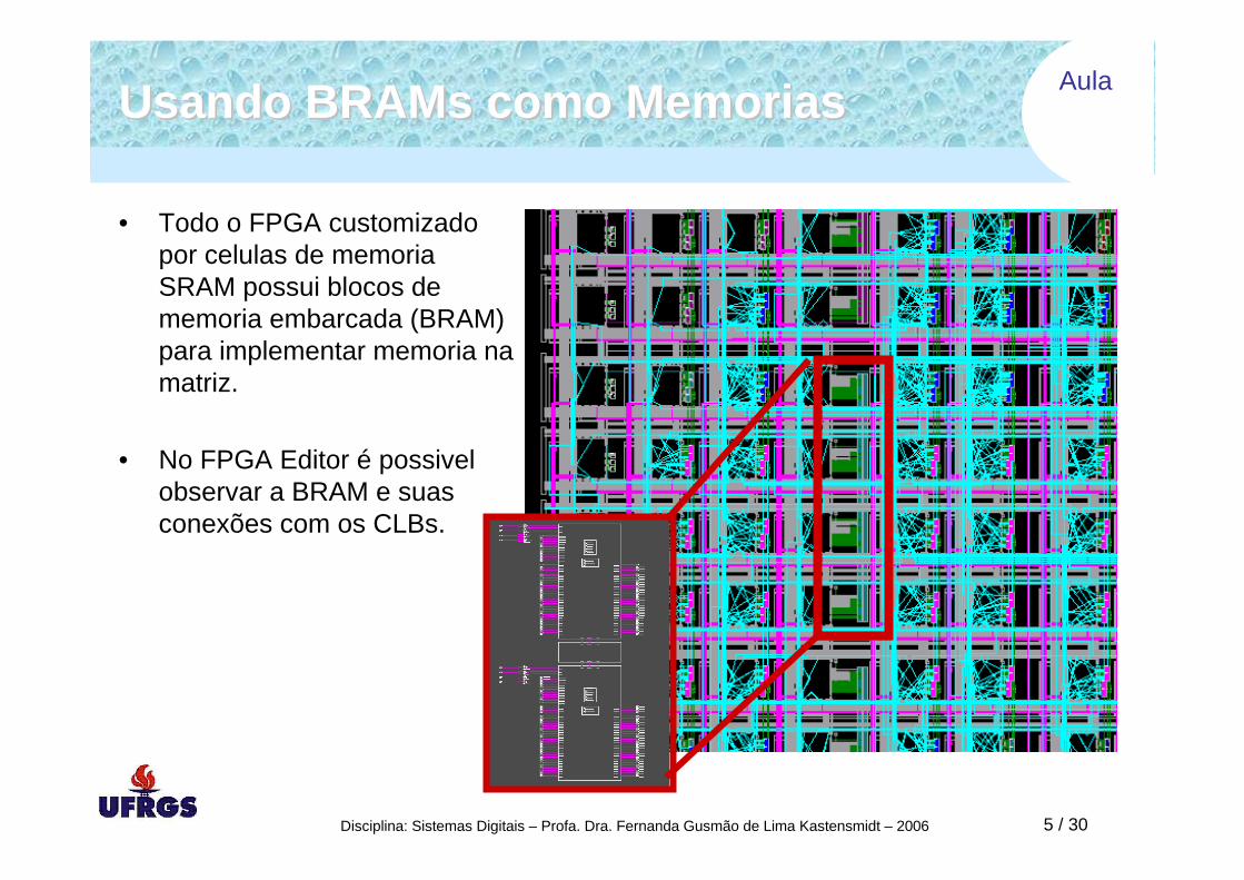
• Todo o FPGA customizadopor celulas de memoriaSRAM possui blocos de memoria embarcada (BRAM) para implementar memoria namatriz.
• No FPGA Editor é possivelobservar a BRAM e suasconexões com os CLBs.
Aula
Disciplina: Sistemas Digitais – Profa. Dra. Fernanda Gusmão de Lima Kastensmidt – 2006 6 / 30
UsandoUsando BRAM BRAM comocomo MemoriasMemorias
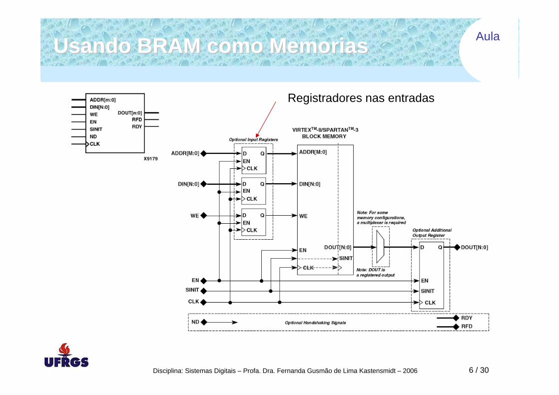
Registradores nas entradas
Aula
Disciplina: Sistemas Digitais – Profa. Dra. Fernanda Gusmão de Lima Kastensmidt – 2006 7 / 30
SinaisSinais dada BRAMBRAM
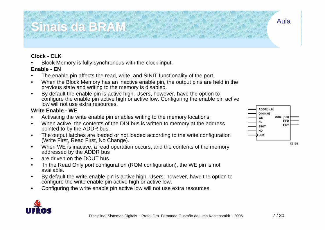
Clock - CLK• Block Memory is fully synchronous with the clock input. Enable - EN• The enable pin affects the read, write, and SINIT functionality of the port. • When the Block Memory has an inactive enable pin, the output pins are held in the
previous state and writing to the memory is disabled.• By default the enable pin is active high. Users, however, have the option to
configure the enable pin active high or active low. Configuring the enable pin active low will not use extra resources.
Write Enable - WE• Activating the write enable pin enables writing to the memory locations. • When active, the contents of the DIN bus is written to memory at the address
pointed to by the ADDR bus. • The output latches are loaded or not loaded according to the write configuration
(Write First, Read First, No Change). • When WE is inactive, a read operation occurs, and the contents of the memory
addressed by the ADDR bus• are driven on the DOUT bus.• In the Read Only port configuration (ROM configuration), the WE pin is not
available.• By default the write enable pin is active high. Users, however, have the option to
configure the write enable pin active high or active low. • Configuring the write enable pin active low will not use extra resources.
Aula
Disciplina: Sistemas Digitais – Profa. Dra. Fernanda Gusmão de Lima Kastensmidt – 2006 8 / 30
SinaisSinais dada BRAMBRAM
Synchronous Initialization - SINIT• When enabled, the SINIT pin forces the data output latches to synchronously load the predefined
SINIT value.• For the Virtex implementation, the SINIT value is zero. Therefore, asserting the SINIT pin causes
the output latches to reset. • For the Virtex-II implementation, the SINIT value is defined by the user. • Consequently, asserting the SINIT pin causes the output latches to contain the user-defined SINIT
value. • This operation does not affect memory locations and does not disturb write operations. • Like the read and write operation, the SINIT function is active only when the enable pin of the port
is active.• By default, the SINIT pin is active high. • Users, however, have the option to configure the SINIT pin active high or active low. • Configuring the write enable pin active low will not use extra resources.Address Bus - ADDR[m:0]• The address bus selects the memory location for read or write access.Data-In Bus - DIN[n:0]• The DIN bus provides the data value to be written into the memory.• Data input and output signals are always buses; that is, in a 1-bit width configuration, the data
input signal is DIN[0] and the data output signal is DOUT[0]. • In the Read Only port configuration (ROM configuration), the DIN bus is not available.Data-Out Bus - DOUT[n:0]• The DOUT bus reflects the contents of memory locations referenced by the address bus during a
read operation.
Aula
Disciplina: Sistemas Digitais – Profa. Dra. Fernanda Gusmão de Lima Kastensmidt – 2006 9 / 30
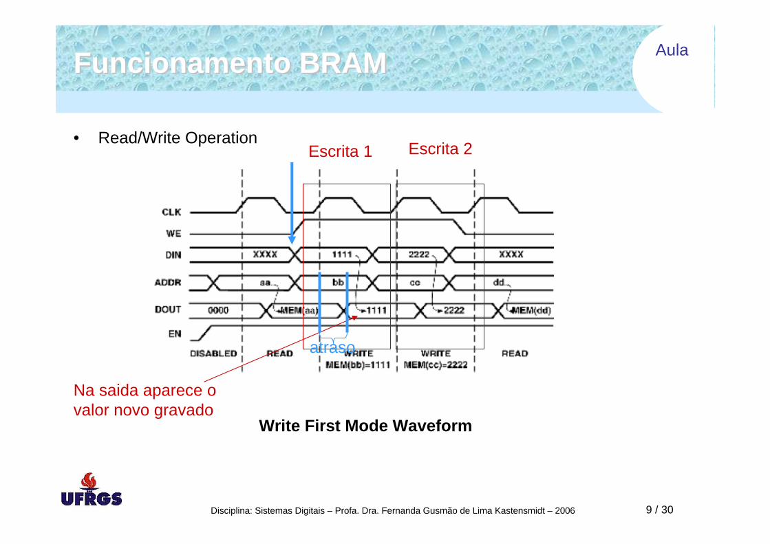
FuncionamentoFuncionamento BRAMBRAM
• Read/Write OperationEscrita 1 Escrita 2
Write First Mode Waveform
Na saida aparece o valor novo gravado
atraso
Aula
Disciplina: Sistemas Digitais – Profa. Dra. Fernanda Gusmão de Lima Kastensmidt – 2006 10 / 30
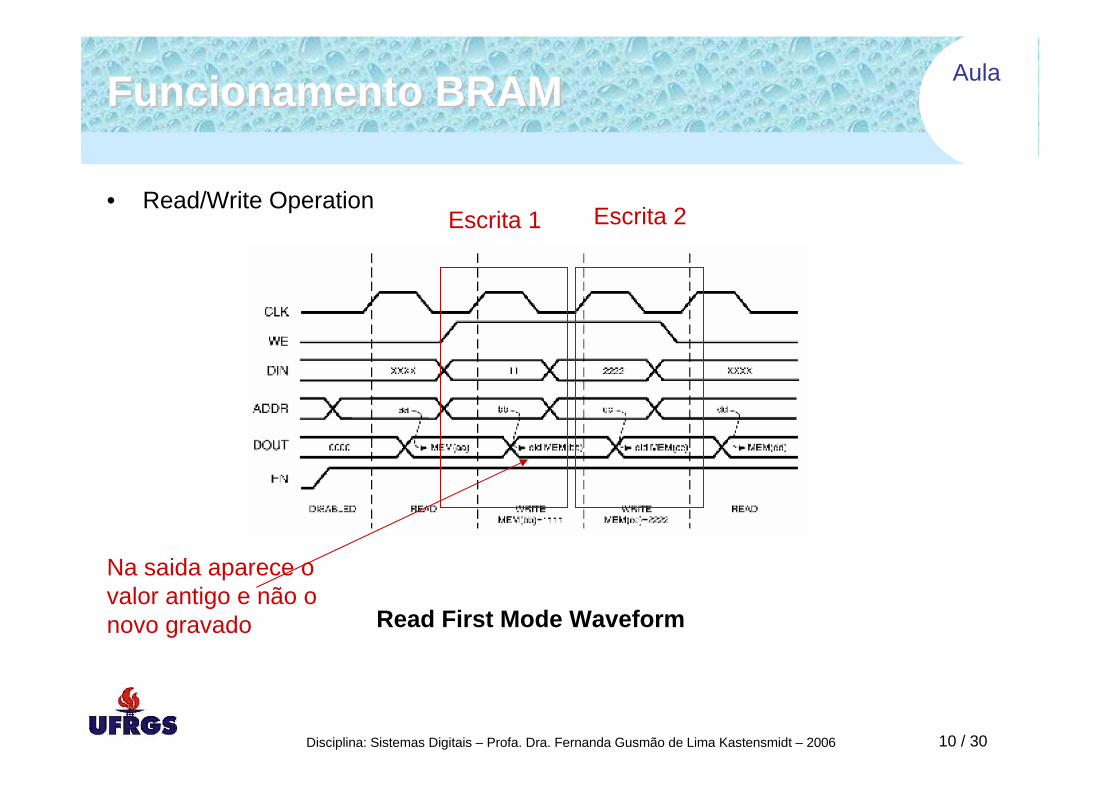
FuncionamentoFuncionamento BRAMBRAM
• Read/Write OperationEscrita 1 Escrita 2
Read First Mode Waveform
Na saida aparece o valor antigo e não o novo gravado
Aula
Disciplina: Sistemas Digitais – Profa. Dra. Fernanda Gusmão de Lima Kastensmidt – 2006 11 / 30
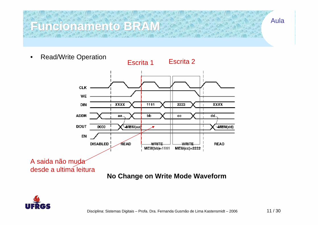
FuncionamentoFuncionamento BRAMBRAM
• Read/Write OperationEscrita 1 Escrita 2
No Change on Write Mode Waveform
A saida não muda desde a ultima leitura
Aula
Disciplina: Sistemas Digitais – Profa. Dra. Fernanda Gusmão de Lima Kastensmidt – 2006 12 / 30
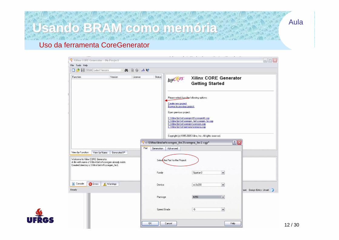
Usando BRAM como memóriaUsando BRAM como memóriaUso da ferramenta CoreGenerator
Aula
Disciplina: Sistemas Digitais – Profa. Dra. Fernanda Gusmão de Lima Kastensmidt – 2006 13 / 30
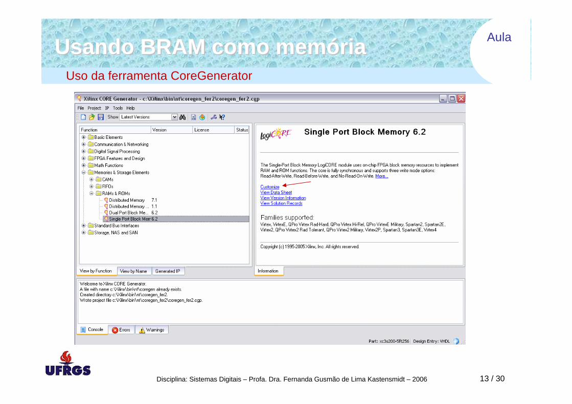
Usando BRAM como memóriaUsando BRAM como memóriaUso da ferramenta CoreGenerator
Aula
Disciplina: Sistemas Digitais – Profa. Dra. Fernanda Gusmão de Lima Kastensmidt – 2006 14 / 30
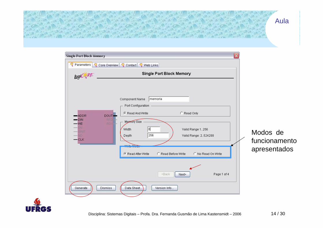
Modos de funcionamentoapresentados
Aula
Disciplina: Sistemas Digitais – Profa. Dra. Fernanda Gusmão de Lima Kastensmidt – 2006 15 / 30
Aula
Disciplina: Sistemas Digitais – Profa. Dra. Fernanda Gusmão de Lima Kastensmidt – 2006 16 / 30
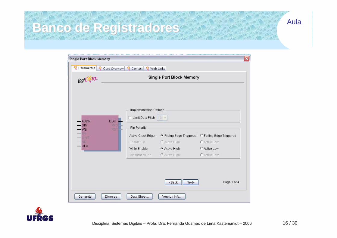
Banco de RegistradoresBanco de Registradores
Aula
Disciplina: Sistemas Digitais – Profa. Dra. Fernanda Gusmão de Lima Kastensmidt – 2006 17 / 30
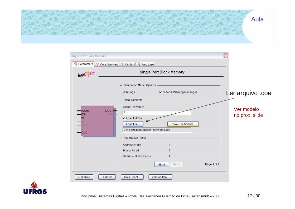
Ler arquivo .coe
Ver modelono prox. slide
Aula
Disciplina: Sistemas Digitais – Profa. Dra. Fernanda Gusmão de Lima Kastensmidt – 2006 18 / 30
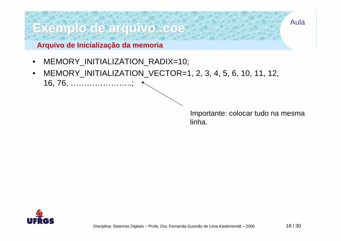
Exemplo de arquivo .coeExemplo de arquivo .coe
• MEMORY_INITIALIZATION_RADIX=10;• MEMORY_INITIALIZATION_VECTOR=1, 2, 3, 4, 5, 6, 10, 11, 12,
16, 76, …………………..;
Importante: colocar tudo na mesmalinha.
Arquivo de Inicialização da memoria
Aula
Disciplina: Sistemas Digitais – Profa. Dra. Fernanda Gusmão de Lima Kastensmidt – 2006 19 / 30
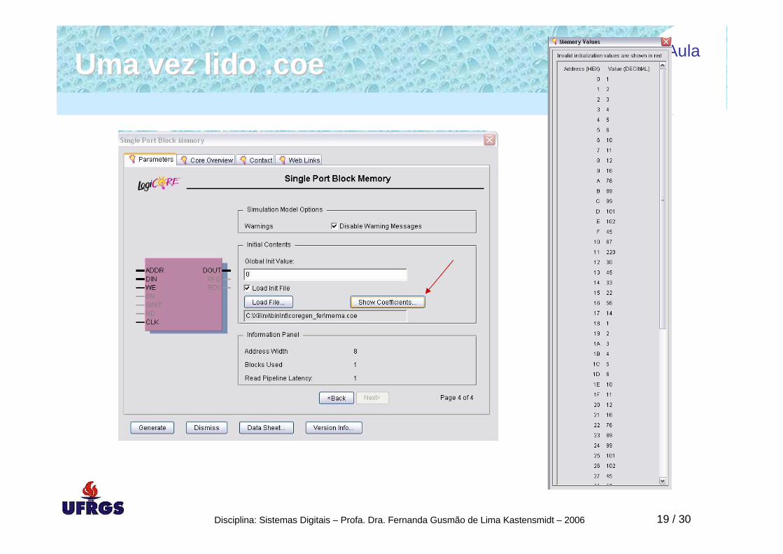
UmaUma vezvez lido .lido .coecoe
Aula
Disciplina: Sistemas Digitais – Profa. Dra. Fernanda Gusmão de Lima Kastensmidt – 2006 20 / 30
Descrição em VHDL de Banco de Reg.Descrição em VHDL de Banco de Reg.
• Banco de registradores é um arranjo de registradores que podemser endereçados de maneira mais direta e rapida, como porexemplo em banco de registadores em um microprocessador.
• Em microprocessadores, um banco de registrador é compostonormalmente por celulas de memoria SRAM, barramento de dados de entrada, saida e endereço e mecanismos parecidos com memoria para leitura e escrita.
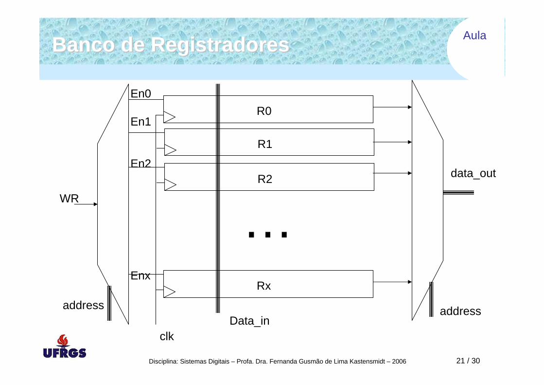
• Em FPGAs, não usamos barramento, logo o arranjo de multiplexadores é organizado de tal forma a usar codificadores e decodificadores no endereço e saida a fim de selecionar o registrador. O barramento dos dados de entrada (data_in) é o mesmo para todos os registradores. De acordo com o sinal de enable (Enx) apenas um registrador por vez armazena o valor do data_in.
Aula
Disciplina: Sistemas Digitais – Profa. Dra. Fernanda Gusmão de Lima Kastensmidt – 2006 21 / 30
BancoBanco de de RegistradoresRegistradores
Rx
R0
R1
R2
…address
clkData_in
address
data_out
En0
En1
En2
Enx
WR
Aula
Disciplina: Sistemas Digitais – Profa. Dra. Fernanda Gusmão de Lima Kastensmidt – 2006 22 / 30
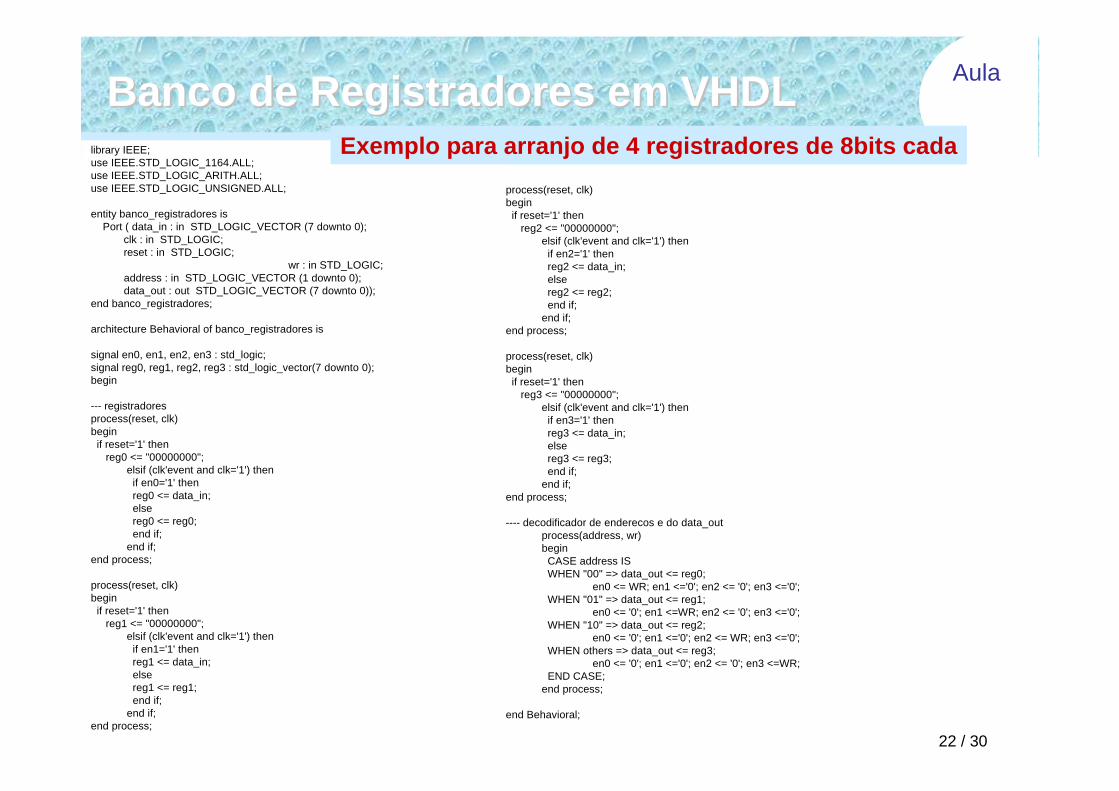
BancoBanco de de RegistradoresRegistradores emem VHDLVHDLlibrary IEEE;use IEEE.STD_LOGIC_1164.ALL;use IEEE.STD_LOGIC_ARITH.ALL;use IEEE.STD_LOGIC_UNSIGNED.ALL;
entity banco_registradores isPort ( data_in : in STD_LOGIC_VECTOR (7 downto 0);
clk : in STD_LOGIC;reset : in STD_LOGIC;
wr : in STD_LOGIC;address : in STD_LOGIC_VECTOR (1 downto 0);data_out : out STD_LOGIC_VECTOR (7 downto 0));
end banco_registradores;
architecture Behavioral of banco_registradores is
signal en0, en1, en2, en3 : std_logic;signal reg0, reg1, reg2, reg3 : std_logic_vector(7 downto 0);begin
--- registradoresprocess(reset, clk)begin
if reset='1' thenreg0 <= "00000000";
elsif (clk'event and clk='1') thenif en0='1' thenreg0 <= data_in;else reg0 <= reg0;end if;
end if;end process;
process(reset, clk)begin
if reset='1' thenreg1 <= "00000000";
elsif (clk'event and clk='1') thenif en1='1' thenreg1 <= data_in;else reg1 <= reg1;end if;
end if;end process;
process(reset, clk)begin
if reset='1' thenreg2 <= "00000000";
elsif (clk'event and clk='1') thenif en2='1' thenreg2 <= data_in;else reg2 <= reg2;end if;
end if;end process;
process(reset, clk)begin
if reset='1' thenreg3 <= "00000000";
elsif (clk'event and clk='1') thenif en3='1' thenreg3 <= data_in;else reg3 <= reg3;end if;
end if;end process;
---- decodificador de enderecos e do data_outprocess(address, wr) begin
CASE address ISWHEN "00" => data_out <= reg0;
en0 <= WR; en1 <='0'; en2 <= '0'; en3 <='0';WHEN "01" => data_out <= reg1;
en0 <= '0'; en1 <=WR; en2 <= '0'; en3 <='0';WHEN "10" => data_out <= reg2;
en0 <= '0'; en1 <='0'; en2 <= WR; en3 <='0';WHEN others => data_out <= reg3;
en0 <= '0'; en1 <='0'; en2 <= '0'; en3 <=WR;END CASE;
end process;
end Behavioral;
Exemplo para arranjo de 4 registradores de 8bits cada
Aula
Disciplina: Sistemas Digitais – Profa. Dra. Fernanda Gusmão de Lima Kastensmidt – 2006 23 / 30
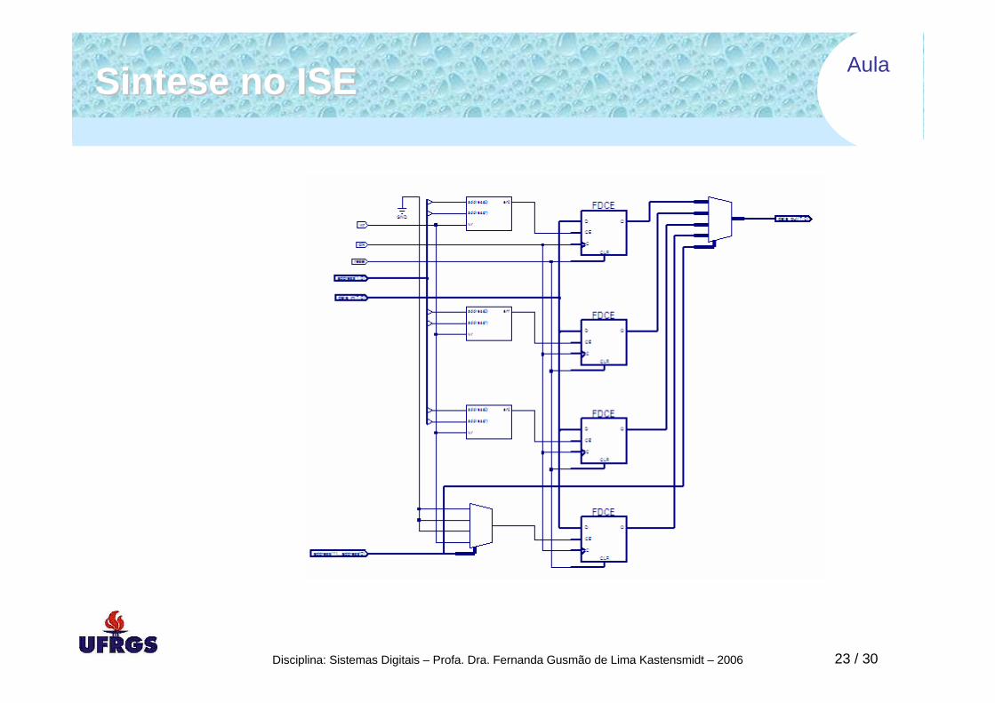
SinteseSintese no ISEno ISE
Aula
Disciplina: Sistemas Digitais – Profa. Dra. Fernanda Gusmão de Lima Kastensmidt – 2006 24 / 30
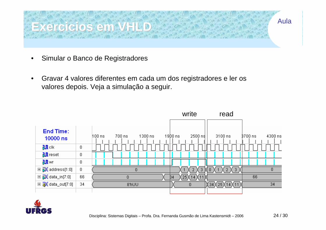
ExerciciosExercicios emem VHLDVHLD
• Simular o Banco de Registradores
• Gravar 4 valores diferentes em cada um dos registradores e ler osvalores depois. Veja a simulação a seguir.
write read
Aula
Disciplina: Sistemas Digitais – Profa. Dra. Fernanda Gusmão de Lima Kastensmidt – 2006 25 / 30
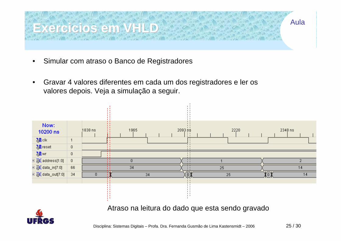
ExerciciosExercicios emem VHLDVHLD
• Simular com atraso o Banco de Registradores
• Gravar 4 valores diferentes em cada um dos registradores e ler osvalores depois. Veja a simulação a seguir.
Atraso na leitura do dado que esta sendo gravado
Aula
Disciplina: Sistemas Digitais – Profa. Dra. Fernanda Gusmão de Lima Kastensmidt – 2006 26 / 30
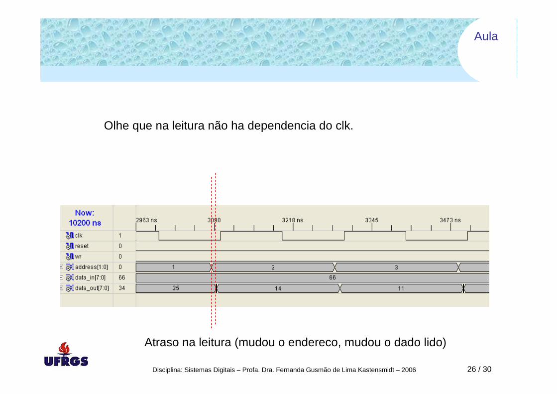
Atraso na leitura (mudou o endereco, mudou o dado lido)
Olhe que na leitura não ha dependencia do clk.
Aula
Disciplina: Sistemas Digitais – Profa. Dra. Fernanda Gusmão de Lima Kastensmidt – 2006 27 / 30
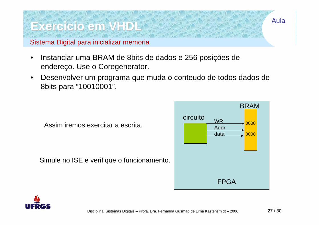
Exercicio em VHDLExercicio em VHDL
• Instanciar uma BRAM de 8bits de dados e 256 posições de endereço. Use o Coregenerator.
• Desenvolver um programa que muda o conteudo de todos dados de 8bits para “10010001”.
BRAM
0000...0000
circuito WRAddrdata
FPGA
Assim iremos exercitar a escrita.
Simule no ISE e verifique o funcionamento.
Sistema Digital para inicializar memoria
Aula
Disciplina: Sistemas Digitais – Profa. Dra. Fernanda Gusmão de Lima Kastensmidt – 2006 28 / 30
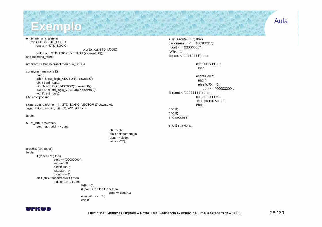
ExemploExemploentity memoria_teste is
Port ( clk : in STD_LOGIC;reset : in STD_LOGIC;
pronto : out STD_LOGIC;dado : out STD_LOGIC_VECTOR (7 downto 0));
end memoria_teste;
architecture Behavioral of memoria_teste is
component memoria ISport (addr: IN std_logic_VECTOR(7 downto 0);clk: IN std_logic;din: IN std_logic_VECTOR(7 downto 0);dout: OUT std_logic_VECTOR(7 downto 0);we: IN std_logic);
END component;
signal cont, dadomem_in: STD_LOGIC_VECTOR (7 downto 0);signal leitura, escrita, leitura2, WR: std_logic;
begin
MEM_INST: memoriaport map( addr => cont,
clk => clk,din => dadomem_in,dout => dado,we => WR);
process (clk, reset)begin
if (reset = '1') thencont <= "00000000";leitura<='0';escrita<='0';leitura2<='0';pronto <='0';
elsif (clk'event and clk='1') thenif (leitura = '0') then
WR<='0';if (cont < "11111111") then
cont <= cont +1;else leitura <= '1';end if;
elsif (escrita = '0') thendadomem_in <= "10010001";
cont <= "00000000";WR<='1';if(cont < "11111111") then
cont <= cont +1;else
escrita <= '1';end if;else WR<= '0';
cont <= "00000000";if (cont < "11111111") then
cont <= cont +1;else pronto <= '1';
end if;end if;end if;end process;
end Behavioral;
Aula
Disciplina: Sistemas Digitais – Profa. Dra. Fernanda Gusmão de Lima Kastensmidt – 2006 29 / 30
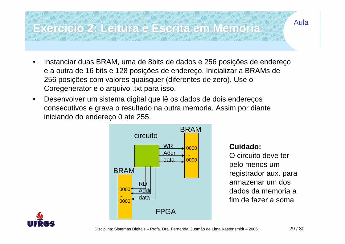
Exercicio 2: Leitura e Escrita em MemoriaExercicio 2: Leitura e Escrita em Memoria
• Instanciar duas BRAM, uma de 8bits de dados e 256 posições de endereço e a outra de 16 bits e 128 posições de endereço. Inicializar a BRAMs de 256 posições com valores quaisquer (diferentes de zero). Use o Coregenerator e o arquivo .txt para isso.
• Desenvolver um sistema digital que lê os dados de dois endereçosconsecutivos e grava o resultado na outra memoria. Assim por diante iniciando do endereço 0 ate 255.
BRAM
0000...0000
circuitoWRAddrdata
FPGA
BRAM
0000...0000
RDAddrdata
Cuidado:O circuito deve ter pelo menos um registrador aux. para armazenar um dos dados da memoria a fim de fazer a soma