Embed Size (px)
Citation preview
V WERICE AEROESPACIAL 2013
Programa e resumos de trabalhos submetidos
São José dos Campos 2013
ORGANIZAÇÃO Coordenação: Odair Lelis Gonçalez, (Instituto de Estudos Avançados) [email protected] Telefone: +55 (12) 3947-5501 Comissão de Programa: Cesar Celeste Ghizoni (Equatorial Sistemas S/A) Claudio Antonio Federico (Instituto de Estudos Avançados) Fernanda Gusmão de Lima Kastensmidt (Universidade Federal do Rio Grande do Sul) Marcilei Aparecida Guazzelli da Silveira (Centro Universitário da FEI) Silvio Manea (Instituto Nacional de Pesquisas Espaciais) Tiago Roberto Balen (Universidade Federal do Rio Grande do Sul) Corpo de Revisores: Ângelo Pássaro (Instituto de Estudos Avançados) Cláudio Antonio Federico (Instituto de Estudos Avançados) Fernanda Gusmão de Lima Kastensmidt (Universidade Federal do Rio Grande do Sul) Gilson Inácio Wirth (Universidade Federal do Rio Grande do Sul) Luiz Henrique Claro (Instituto de Estudos Avançados) Marcilei Aparecida Guazzelli da Silveira (Centro Universitário da FEI) Nemitala Added (Universidade de São Paulo) Nilberto Heder Medina (Universidade de São Paulo) Odair Lelis Gonçalez (Instituto de Estudos Avançados) Tiago Roberto Balen (Universidade Federal do Rio Grande do Sul) Comitê Local: Adriane Cristina Mendes Prado (Instituto de Estudos Avançados) Evaldo Carlos Fonseca Pereira Júnior (Instituto de Estudos Avançados) Heloisa Helena de Castilho Pereira (Instituto de Estudos Avançados) Jéssica de Freitas Cipeli (Instituto de Estudos Avançados) Marlon Antonio Pereira (Instituto de Estudos Avançados) Rafael Galhardo Vaz (Instituto de Estudos Avançados) Contatos: [email protected]

V WERICE AEROESPACIAL 2013 São José dos Campos, SP, Brazil, October 21-23, 2013 INSTITUTO DE ESTUDOS AVANÇADOS - IEAv
PROGRAMA DO V WERICE AEROESPACIAL 2013 V WORKSHOP SOBRE OS EFEITOS DAS RADIAÇÕES IONIZANTES EM COMPO NENTES
ELETRÔNICOS E FOTÔNICOS DE USO AEROESPACIAL
21 de outubro de 2013 Sessão institucional
Horário Programa
8:30 − 9:00 Acesso e credenciamento 9:00 − 10:00 Abertura solene: Diretor-Geral do Departamento de Ciência e
Tecnologia Aeroespacial (DCTA) e autoridades convidadas 10:00 − 10:30 Coffee-break e posteres 10:30 − 11:10 Palestra de abertura: "O Programa Nacional de Atividades
Espaciais 2012-2021" Carlos Alberto Gurgel Veras (Agência Espacial Brasileira −AEB)
11:10 − 11:50 Palestra: "Programa de Satélites Científicos" Leonel Fernando Perondi (Instituto Nacional de Pesquisas Espaciais − INPE)
11:50 – 12:30 Palestra: "Componentes eletrônicos para aplicações aeroespaciais, uma questão estratégica na visão do programa INOVA AERODEFESA" ( Título a confirmar) Ricardo Gonzaga Martins de Araújo (Agência Brasileira de Desenvolvimento Industrial, GT Brasil Maior, Programa Inova Aerodefesa)
12:30 − 14:00 Almoço 14:00 – 14:40 Palestra: 'Radiação cósmica no Espaço Aéreo Brasileiro:
Dosimetria no interior da aeronave e os efeitos em aviônicos" Cláudio Antonio Federico (Instituto de Estudos Avançados − IEAv)
14:40 – 15:00 Apresentação Institucional: “Novos Processos de desenvolvimento de aviônicos resultantes dos efeitos da radiação e a IEC TS 62396-1” Marcos Osmar Arend (AEL Sistemas)
15:00 – 15:20 Apresentação Institucional: " FGPA Techniques for Aerospace and Avionics " Luigi Lauro (Anacom Eletrônica)
15:20 – 15:40 Apresentação institucional: "O Projeto CITAR: Desenvolvimento de CI's robustos e tolerantes à radiação" Saulo Finco (Centro de Tecnologia da Informação Renato Archer − CTI)
15:40 – 16:00 Coffee-break e posteres 16:00 − 17:00 Palestra: "Lei da Inovação e fontes de financiamento oficiais para
P,D&I nas empresas e instituições de ensino e pesquisa" Vagner Bernal Barbeta (IPEI – Instituto de Pesquisas e Estudos Industriais, FEI)
17:00 − 18:00 Encerramento: "Mesa redonda P,D&I no Brasil em eletrônica robusta e tolerante à radiação para aplicações aeroespaciais."
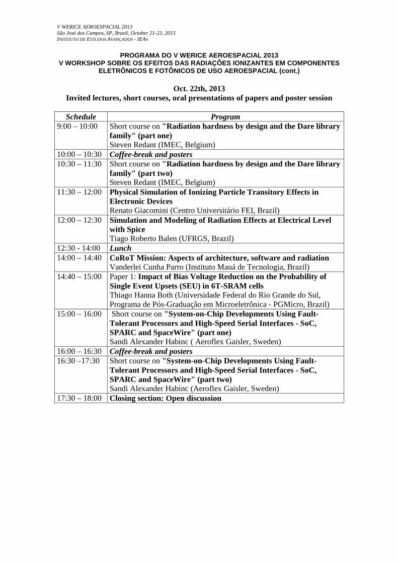
V WERICE AEROESPACIAL 2013 São José dos Campos, SP, Brazil, October 21-23, 2013 INSTITUTO DE ESTUDOS AVANÇADOS - IEAv
PROGRAMA DO V WERICE AEROESPACIAL 2013 V WORKSHOP SOBRE OS EFEITOS DAS RADIAÇÕES IONIZANTES EM COMPO NENTES
ELETRÔNICOS E FOTÔNICOS DE USO AEROESPACIAL (cont.)
Oct. 22th, 2013 Invited lectures, short courses, oral presentations of papers and poster session
Schedule Program
9:00 – 10:00 Short course on "Radiation hardness by design and the Dare library family" (part one) Steven Redant (IMEC, Belgium)
10:00 – 10:30 Coffee-break and posters 10:30 – 11:30 Short course on "Radiation hardness by design and the Dare library
family" (part two) Steven Redant (IMEC, Belgium)
11:30 – 12:00 Physical Simulation of Ionizing Particle Transitory Effects in Electronic Devices Renato Giacomini (Centro Universitário FEI, Brazil)
12:00 – 12:30 Simulation and Modeling of Radiation Effects at Electrical Level with Spice Tiago Roberto Balen (UFRGS, Brazil)
12:30 - 14:00 Lunch 14:00 – 14:40
CoRoT Mission: Aspects of architecture, software and radiation Vanderlei Cunha Parro (Instituto Mauá de Tecnologia, Brazil)
14:40 – 15:00 Paper 1: Impact of Bias Voltage Reduction on the Probability of Single Event Upsets (SEU) in 6T-SRAM cells Thiago Hanna Both (Universidade Federal do Rio Grande do Sul, Programa de Pós-Graduação em Microeletrônica - PGMicro, Brazil)
15:00 – 16:00 Short course on "System-on-Chip Developments Using Fault-Tolerant Processors and High-Speed Serial Interfaces - SoC, SPARC and SpaceWire" (part one) Sandi Alexander Habinc ( Aeroflex Gaisler, Sweden)
16:00 – 16:30 Coffee-break and posters 16:30 –17:30 Short course on "System-on-Chip Developments Using Fault-
Tolerant Processors and High-Speed Serial Interfaces - SoC, SPARC and SpaceWire" (part two) Sandi Alexander Habinc (Aeroflex Gaisler, Sweden)
17:30 – 18:00 Closing section: Open discussion
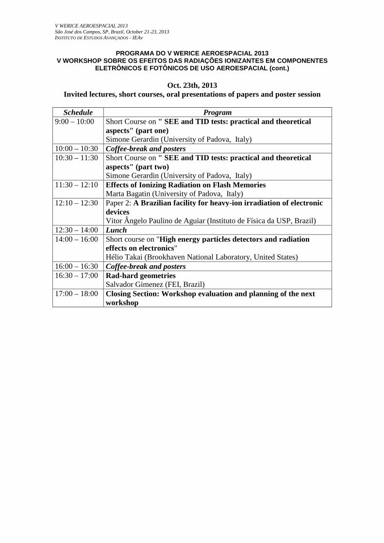
V WERICE AEROESPACIAL 2013 São José dos Campos, SP, Brazil, October 21-23, 2013 INSTITUTO DE ESTUDOS AVANÇADOS - IEAv
PROGRAMA DO V WERICE AEROESPACIAL 2013 V WORKSHOP SOBRE OS EFEITOS DAS RADIAÇÕES IONIZANTES EM COMPO NENTES
ELETRÔNICOS E FOTÔNICOS DE USO AEROESPACIAL (cont.)
Oct. 23th, 2013 Invited lectures, short courses, oral presentations of papers and poster session
Schedule Program
9:00 – 10:00 Short Course on " SEE and TID tests: practical and theoretical aspects" (part one) Simone Gerardin (University of Padova, Italy)
10:00 – 10:30 Coffee-break and posters 10:30 – 11:30 Short Course on " SEE and TID tests: practical and theoretical
aspects" (part two) Simone Gerardin (University of Padova, Italy)
11:30 – 12:10 Effects of Ionizing Radiation on Flash Memories Marta Bagatin (University of Padova, Italy)
12:10 – 12:30 Paper 2: A Brazilian facility for heavy -ion irradiation of electronic devices Vitor Ângelo Paulino de Aguiar (Instituto de Física da USP, Brazil)
12:30 – 14:00 Lunch 14:00 – 16:00
Short course on "High energy particles detectors and radiation effects on electronics" Hélio Takai (Brookhaven National Laboratory, United States)
16:00 – 16:30 Coffee-break and posters 16:30 – 17:00 Rad-hard geometries
Salvador Gimenez (FEI, Brazil) 17:00 – 18:00 Closing Section: Workshop evaluation and planning of the next
workshop
V WERICE AEROESPACIAL 2013 São José dos Campos, SP, Brazil, October 21-23, 2013 INSTITUTO DE ESTUDOS AVANÇADOS - IEAv
V WERICE AEROESPACIAL 2013 São José dos Campos, SP, Brazil, October 21-23, 2013 INSTITUTO DE ESTUDOS AVANÇADOS - IEAv
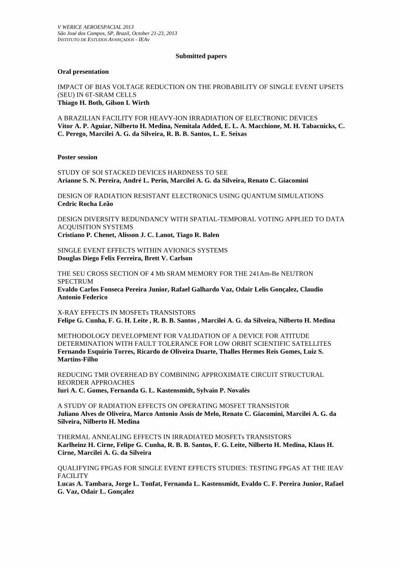
Submitted papers Oral presentation IMPACT OF BIAS VOLTAGE REDUCTION ON THE PROBABILITY OF SINGLE EVENT UPSETS (SEU) IN 6T-SRAM CELLS Thiago H. Both, Gilson I. Wirth A BRAZILIAN FACILITY FOR HEAVY-ION IRRADIATION OF ELECTRONIC DEVICES Vitor A. P. Aguiar, Nilberto H. Medina, Nemitala Added, E. L. A. Macchione, M. H. Tabacnicks, C. C. Perego, Marcilei A. G. da Silveira, R. B. B. Santos, L. E. Seixas Poster session STUDY OF SOI STACKED DEVICES HARDNESS TO SEE Arianne S. N. Pereira, André L. Perin, Marcilei A. G. da Silveira, Renato C. Giacomini DESIGN OF RADIATION RESISTANT ELECTRONICS USING QUANTUM SIMULATIONS Cedric Rocha Leão DESIGN DIVERSITY REDUNDANCY WITH SPATIAL-TEMPORAL VOTING APPLIED TO DATA ACQUISITION SYSTEMS Cristiano P. Chenet, Alisson J. C. Lanot, Tiago R. Balen SINGLE EVENT EFFECTS WITHIN AVIONICS SYSTEMS Douglas Diego Felix Ferreira, Brett V. Carlson THE SEU CROSS SECTION OF 4 Mb SRAM MEMORY FOR THE 241Am-Be NEUTRON SPECTRUM Evaldo Carlos Fonseca Pereira Junior, Rafael Galhardo Vaz, Odair Lelis Gonçalez, Claudio Antonio Federico X-RAY EFFECTS IN MOSFETs TRANSISTORS Felipe G. Cunha, F. G. H. Leite , R. B. B. Santos , Marcilei A. G. da Silveira, Nilberto H. Medina METHODOLOGY DEVELOPMENT FOR VALIDATION OF A DEVICE FOR ATITUDE DETERMINATION WITH FAULT TOLERANCE FOR LOW ORBIT SCIENTIFIC SATELLITES Fernando Esquírio Torres, Ricardo de Oliveira Duarte, Thalles Hermes Reis Gomes, Luiz S. Martins-Filho REDUCING TMR OVERHEAD BY COMBINING APPROXIMATE CIRCUIT STRUCTURAL REORDER APPROACHES Iuri A. C. Gomes, Fernanda G. L. Kastensmidt, Sylvain P. Novalès A STUDY OF RADIATION EFFECTS ON OPERATING MOSFET TRANSISTOR Juliano Alves de Oliveira, Marco Antonio Assis de Melo, Renato C. Giacomini, Marcilei A. G. da Silveira, Nilberto H. Medina THERMAL ANNEALING EFFECTS IN IRRADIATED MOSFETs TRANSISTORS Karlheinz H. Cirne, Felipe G. Cunha, R. B. B. Santos, F. G. Leite, Nilberto H. Medina, Klaus H. Cirne, Marcilei A. G. da Silveira QUALIFYING FPGAS FOR SINGLE EVENT EFFECTS STUDIES: TESTING FPGAS AT THE IEAV FACILITY Lucas A. Tambara, Jorge L. Tonfat, Fernanda L. Kastensmidt, Evaldo C. F. Pereira Junior, Rafael G. Vaz, Odair L. Gonçalez
V WERICE AEROESPACIAL 2013 São José dos Campos, SP, Brazil, October 21-23, 2013 INSTITUTO DE ESTUDOS AVANÇADOS - IEAv
PERFORMANCE OF A HIGH SPEED PIPELINE ADC UNDER IRRADIATION FOR HIGH ENERGY PHYSICS APPLICATIONS Marco A. L. Leite, Eduardo L. A. Macchione , Olacio Dietzsch, Ricardo Menegasso, Marcel K. Kuriyama, Odair L. Gonçalez, Rafael G. Vaz, Evaldo C. F. Pereira Junior IMPACT OF BIAS VOLTAGE REDUCTION ON THE PROBABILITY OF SINGLE EVENT UPSETS (SEU) IN 6T-SRAM CELLS Thiago H. Both, Gilson I. Wirth A BRAZILIAN FACILITY FOR HEAVY-ION IRRADIATION OF ELECTRONIC DEVICES Vitor A. P. Aguiar, Nilberto H. Medina, Nemitala Added, E. L. A. Macchione, M. H. Tabacnicks, C. C. Perego, Marcilei A. G. da Silveira, R. B. B. Santos, L. E. Seixas
V WERICE AEROESPACIAL 2013 São José dos Campos, SP, Brazil, October 21-23, 2013 INSTITUTO DE ESTUDOS AVANÇADOS - IEAv
KEYWORDS: SEE; SOI; Stacked device
STUDY OF SOI STACKED DEVICES HARDNESS TO SEE
Arianne S. N. Pereira1*, André L. Perin1,2, Marcilei Guazzeli1,3 and Renato C. Giacomini1
1 Centro Universitário da FEI
São Bernardo do Campo – SP – Brasil *[email protected]
2 Universidade Metodista de São Paulo São Bernardo do Campo – SP – Brasil
3 Universidade de São Paulo
São Paulo – SP – Brasil
ABSTRACT
The radiation effects on semiconductors have been widely investigated, mostly for space environment applications, where the device is exposed to many radiation sources. The effect caused by a single particle striking the device is called Single-Event Effect (SEE), which can be permanent or transitory. This work addresses transitory effects, particularly the Single-Event Upset (SEU), which is a change in the logic state of a memory cell and the Single-Event Transient (SET), which is a transient pulse present in an input or output of a combinational circuit. In MOS (Metal Oxide Semiconductor) transistors, the sensitivity to radiation is related to its active semiconductor volume, in other words, the smaller the active volume, the lower the susceptibility to SEE. Silicon-On-Insulator (SOI) technology refers to the use of a layered silicon-insulator-silicon substrate in place of conventional silicon substrates in semiconductor manufacturing. The transistors are built in the silicon film that is delimited at the bottom by the buried insulator, which is usually silicon dioxide. Indeed, such silicon dioxide layer insulates all the SOI transistors from the substrate and from each other. SOI devices are, consequently, less sensitive to radiation effects than conventional MOS devices, due to their reduced active volume and the isolation from the substrate. Other advantage of this technology is the absence of latch-up, an undesired behavior of CMOS (Complementary Metal Oxide Semiconductor) circuits caused by the proximity of n and p-channel transistors sharing the same substrate without dielectric insulation. Some especial circuit architectures can be used to reduce even more the SOI SEE susceptibility. One of these is the use of a stacked array, which is a series connection of two transistors. Previous works show that stacked transistor arrays on SOI technology have the potential to provide reliable designs regarding single-event upset. In a stacked array set to the off state, one of the transistors can be kept off, when the other is turned on by the charge generated in the semiconductor active region by the particle. Therefore, the stacked array is tolerant to some single-particle effects. This work compares the SEE hardness of two SOI stacked device configurations (layouts): the first one is designed sharing one silicon region as the source of one transistor and the drain of the other. Two electrically connected transistors with conventional layouts compose the second configuration. Both configurations were described in Atlas tridimensional device simulator. The drain current, potential, electron concentration and hole concentration of the two stacked configurations were observed as functions of time when the particle crosses the structure, for several different paths and incidence angles. The stacked configuration with conventional layouts showed to be the hardest one, because the shared source and drain configuration changes its logical state for most particle paths.
V WERICE AEROESPACIAL 2013 São José dos Campos, SP, Brazil, October 21-23, 2013 INSTITUTO DE ESTUDOS AVANÇADOS - IEAv
KEYWORDS: Radiation Stable Electronics; Heterostructures; Density Functional Theory
DESIGN OF RADIATION RESISTANT ELECTRONICS USING QUA NTUM SIMULATIONS
Cedric Rocha Leão*
Universidade Federal do ABC (UFABC) Santo André – SP – Brasil
ABSTRACT
Some tetrahedrally coordinate compounds crystallize in the so called “defective zinc-blend” structure, in which sites of the cation sublatice remain vacant. These are called “stoichiometric vacancies” and their occurrence is governed exclusively by valence conditions regardless of temperature and other crystal growth parameters. These materials with a “loose” crystal structure poses interesting properties. Whereas most semiconductors suffer dramatic changes in their electronic properties after irradiation of 1012 - 1014 fast neutrons per cm2, this type of materials have been shown to remain unaffected by radiation doses of up to 1018 - 1019 fast neutrons per cm2. The reason for that is the barrierless capacity of such materials to self-heal radiation generated defects, due to their loose lattice structure. This characteristic that makes such materials desirable for extreme conditions electronics also introduces a seemingly unsolvable limitation, which is a material that remains invariably intrinsic regardless the doping levels one can achieve. This is so because dopant atoms tend to be incorporated in the stoichiometric vacancy sites, where they are virtually shielded from the crystalline environment they are embedded in, remaining non-ionized and thus electronically inert. Heterostructures can be used as a way to introduce carriers in a material without using dopants, having the advantage of not adding the scattering centers that the former ones necessarily do. However, for heterostructures to be viable and useful the materials need to have the right properties, such as similar lattice parameters and crystal structures to minimize strain, the right band-gaps and more importantly, the right band-offset, which is the difference in the alignment of the band edges on the two materials. This offset causes band-bending on both sides of the heterojunction, so that free carriers can be introduced without doping. Electrical current along the junction plane can be thus achieved, with carriers of opposite signals on each side of it. In this work, we discuss in general grounds the viability of this mechanism using materials with stoichiometric vacancies for radiation stable electronics. Inspection on the pristine materials should indicate the most suitable matches according to their structural and electronic properties, such as lattice mismatch, band-gaps and mobility of carriers. Questions regarding the pristine materials remain unanswered, as for example whether these vacancies present some kind of ordering or are randomly distributed as well as how this might affect their electronic properties. Stoichiometric vacancies, although electronically inert, possibly can scatter carriers, mainly in the absence of ordering. We can investigate heterostructures of these materials. Since the interfacial dipole is crucial for heterostructures, we will analyze junctions of films with different orientations, <111>, <110>, <100>, evaluating their band-offsets in order to asses how suitable they are for the formation of pn-junctions and eventually other types of electronic devices. Although defects in the intrinsic materials seem not to affect their electronic properties, the same might not be true in the case of interface defects. Density functional based simulations provide a viable way to access these effects.
V WERICE AEROESPACIAL 2013 São José dos Campos, SP, Brazil, October 21-23, 2013 INSTITUTO DE ESTUDOS AVANÇADOS - IEAv
KEYWORDS: fault tolerance; design diversity redundancy; analog-to-digital converters
DESIGN DIVERSITY REDUNDANCY WITH SPATIAL-TEMPORAL V OTING APPLIED TO DATA ACQUISITION SYSTEMS
Cristiano P. Chenet, Alisson J. C. Lanot and Tiago R. Balen
Universidade Federal do Rio Grande do Sul (UFRGS) Porto Alegre – RS – Brasil
{cristiano.chenet, alisson.lanot, tiago.balen}@ufrgs.br
ABSTRACT
Modern circuits are subject to the aging phenomenon, radiation effects, electromagnetic interference and other environmental interactions. For example, in programmable analog technologies susceptible to radiation exposure, the inversion of a single programming bit by Single Event Upset (SEU) may be catastrophic to the functionality. Thus, in applications that require rigor at performance, availability and reliability, such as avionics or medical systems, it is important to reduce the probability of failure to the minimum possible. The techniques used to add fault tolerance to electronic system are usually based on hardware and/or time redundancy. Among these techniques, the most popular is the Triple Modular Redundancy (TMR), which consists on triplicating the designed circuit and feeding a majority voter with the outputs of these circuits. In case of error in one of the triplicated blocks, two of them continue operating properly and the correct value is chosen by the voter. An enhanced technique is the Diversity Triple Modular Redundancy (DTMR), in which each block is built with different architectures. The different levels of resilience from each block reduce the probability of multiple faults to affect different blocks, increasing the system fault tolerance. The present work addresses the application of the concept of DTMR to Analog-to-Digital Converters (ADCs). A physical implementation of the system is made in a single programmable mixed-signal device: the Programmable System-On-Chip CY8C5588AXI-060, belonging to PSoC5 family from Cypress Semiconductor. The diversity is implemented by using a Sigma-Delta ADC with sample frequency (fs) of 100 kHz, a Successive Approximation Register (SAR) ADC, also with fs = 100 kHz, and an SAR ADC running at 1 MHz. The two different types of ADCs form a hardware diversity redundancy scheme and the two different sampling frequencies can be used in a time redundancy approach. As the SAR ADC running at 1 MHz has its sampling rate ten times higher than the other ADCs, there is a voter at its output that generates one digital word for every ten input samples. This word and the samples from the other ADCs feed the main voter, which produce the system output. Both voters are designed in software, running on the PSoC microprocessor. To evaluate the system, simulations were performed in a way that single and multiple deviations caused by bit-inversions were injected into the output of each ADC, while the system output was monitored. Results indicate that the system is able to detect 100% of single bit-flip faults. Injection of multiple bit-flips is being performed and results will be presented in the final paper. As future works, the system will be irradiated with neutrons, to validate quantitatively the effectiveness of the proposed system and the DTMR concept.
V WERICE AEROESPACIAL 2013 São José dos Campos, SP, Brazil, October 21-23, 2013 INSTITUTO DE ESTUDOS AVANÇADOS - IEAv
KEYWORDS: Single Event Effects; SEE; Avionics
SINGLE EVENT EFFECTS WITHIN AVIONICS SYSTEMS
Douglas Diego Felix Ferreira*, Brett V. Carlson
Instituto Tecnológico de Aeronáutica (ITA) São José dos Campos – SP – Brasil
ABSTRACT
This work aims to assess the potential safety issues caused by Single Event Effects (SEE) within avionics systems. Cosmic radiation, from solar and galactic sources, interacts with the atmosphere generating a cascade of secondary particles composed mainly by neutrons, which can trigger adverse effects in electronic equipment. Commercial aircraft can reach altitudes above 40,000 ft during cruise, where the levels of radiation are 300 times higher than that observed on ground. The Earth's magnetic field funnel down and accelerate charged particles of the solar wind along the magnetic field lines, creating the aurorae in the poles. Those particles can also affect computer-based systems of aircraft flying polar routes. Orbiting satellites have higher SEE rates when passing through the South Atlantic Anomaly (SAA), a region where the Van Hallen belt comes closest to the Earth's surface resulting in a high flux of energetic particles. Flights between South America and Europe often pass the SAA area. The increased use of embedded systems in commercial aircraft (mainly driven by the fly-by-wire technology), the use of polar routes by airliners and the reduction of the transistor size in integrated circuits tends to increase the susceptibility of avionics to radiation effects. Guidelines concerning SEE in this domain are being released by aviation authorities and other organizations. A brief introduction of the atmospheric radiation is presented, with the classification of different types of SEE, mitigation techniques and how the SEE assessment can be incorporated in the development and certification processes for future commercial aircraft.
V WERICE AEROESPACIAL 2013 São José dos Campos, SP, Brazil, October 21-23, 2013 INSTITUTO DE ESTUDOS AVANÇADOS - IEAv
KEYWORDS: SEU; SRAM memory; fast neutrons
THE SEU CROSS SECTION OF 4 Mb SRAM MEMORY FOR THE 241Am-Be NEUTRON SPECTRUM
Evaldo Carlos Fonseca Pereira Junior*, Rafael Galhardo Vaz, Odair Lelis Gonçalez e Claudio
Antonio Federico
Instituto de Estudos Avançados (IEAv) São José dos Campos – SP – Brasil
ABSTRACT
Electronic instruments operating under ionizing radiation suffer adverse effects on its performance, resulted by the interaction of radiation with its basic components. In electronic circuits, these effects appear as transient or permanent deviations of electrical parameters of the circuit, malfunction or even complete failure of the system. These effects can be classified as transient or cumulative and may also be reversible or not reversible. The transient effects are usually associated with rapid collection of electric charges released in a sensitive region of the device by the passage of a heavy ionizing particle, causing a spurious electrical pulse in the circuit node reached (Single Event Effects, or briefly, SEE). In digital circuits the most important SEE is the "bit flip" in logic cells, named Single Event Upset (SEU). For SEE tests, high energy particle accelerators are employed in order to determine the thresholds and cross sections for each type of SEE caused by protons and heavy ions, as a function of the linear energy transfer (LET) of these particles in the device material. The SEE cross section is a function of particle LET, according the Weibull type curve and it is independent of the type of incident particle. The ionization of the medium by neutrons is caused by energetic ions coming from collisions and nuclear reactions produced by the interactions of incident neutrons with the nuclei of the atoms constituents of the medium. Therefore, is not possible to associate a continuous linear energy transfer along the neutron path into the medium in the same way that it is associated to charged heavy particles. The dosimetric quantity corresponding to the LET, for the interaction of neutrons with the medium, is the KERMA (Kinetic Energy Released in Matter). However, in the case of microdosimetry, as would applied to electronic microcomponents, in which is necessary to associate the energy deposited continuously by a single incoming particle with the ion pairs generated along its path, this dosimetric quantity (KERMA) could not adequately applied to determine the medium ionization in a very small volume, whose electrical charges would be responsible for the SEE. The reason is the probabilistic nature of the neutron interactions with nuclei of material atoms. Thus the SEE neutron cross section should be expressed as a function of neutron energy and should not follow exactly a step function with threshold described by the Weibull fit curve. Most SEE experiments are performed with high energy neutrons from spallation sources due to the interest in the effects in electronic instrumentation produced by secondary cosmic radiation (mainly neutrons) on ground and at flight altitudes, whose neutron energy spectrum extends up to 400 MeV. Also, the IEC specifications consider of greatest concern the neutron energy range above 10 MeV. However, there is a significant contribution from neutrons produced by nuclear evaporation process with energy below 10 MeV (low energy end point of intranuclear cascade) in the cosmic-ray-induced neutron spectrum in the atmosphere and on the ground, Thus, both for studies of fast neutron effects in electronic components produced by cosmic radiation in the atmosphere, as well for other nuclear applications (e.g., reactors), the region below 10 MeV is of particular interest. Besides a detailed description of the behavior of the neutron SEE cross section near its threshold should significantly improve the accuracy of calculations of SEE forecast for purposes of flight safety in aeronautical applications. This paper presents the results of SEU measures on a 4 Mb SRAM memory of 0.130 µm technology irradiated with fast neutrons from eight 100 mCi 241Am-Be radioactive sources, whose energy spectrum ranges from keV units up to 10.8 MeV. The neutron irradiations were carried out in stages and between each stage of neutron irradiation, the memory was irradiated with 60Co gamma rays, in order to verify possible effects of TID aging, also.
V WERICE AEROESPACIAL 2013 São José dos Campos, SP, Brazil, October 21-23, 2013 INSTITUTO DE ESTUDOS AVANÇADOS - IEAv
KEYWORDS: MOSFETs;X-RAY;Radiation
X-RAY EFFECTS IN MOSFETs TRANSISTORS
Felipe G. Cunha1, F.G.H.Leite1 , R.B.B. Santos1 , Marcilei A. G. da Silveira1 and M.H.Medina2
1 Centro Universitário da FEI (FEI)
São Bernardo do Campo – SP – Brasil *[email protected]
2 Universidade de São Paulo (USP)
São Paulo– SP – Brasil
ABSTRACT
MOSFET (Metal Oxide Semiconductor Field Effect Transistor) technology began its development on the 70`s and is, still, the most employed transistor to amplify electric signals. The technology is based upon a four terminal device, one of which a closed circuit that works when tension is applied between the gate and the source, generating an electric field which penetrates the oxide creating a channel between the source and the drain that in turns creates a channel where the electrical current flows. Electronic devices are increasingly exposed to ionizing radiation thanks to its use on the most varied environments. Some of them might have to work on environments where the exposal is higher and thus resulting in changes on its characteristics and basic settings due to the radiation interaction with the devices. The effects might be either transient or permanent, and are increasingly tangible due to the device trend to get smaller and smaller. The cumulative effects are possibly reversible by using some methods as, for example, annealing, although, most of the time, the effects are not reversible, while transient effects cause momentary problems as, for example, changes on stored data or even peaks on electrical current that might damage the electrical circuit. These effects may be observed by three different mechanisms: i) accumulate electrical charges in sensitive parts, in this case, the gate oxide and on the oxide-silicon interface, due to the limited mobility on the holes that got trapped causing reminiscent tension; ii) great energy accumulated in a restricted device’s area resulting on a high charge density region, usually when the device gets exposed to radiation provided by high Linear Energy Transfer; iii) imperfections generated on the silicon crystalline atomic structure, creating unbalanced positions. All those mechanisms are named Total Ionization Dose (TID), Single Event Effects (SEE), and Displacement Damage (DD), respectively. With the increasing need to develop devices that are tolerant to these effects, ground characterization becomes increasingly important, thus, here, we study the voltage threshold variation obtained from drain current and gate voltage data of a device as it is exposed to different X-ray radiation doses. Thus, we developed a study based on TID mechanisms. We used aCD4007 Integrated Circuit, which is composed by six Field Effect Transistors, three of them N-type transistors, and three P-type transistors. Therefore, we expected to observe how the radiation affects the device, depending on the transistor type utilized on the transistor manufacturing. The irradiations where performed at Centro Universitario da FEI, Brazil. The measurements where made using an Agilent HP 4156C device. It was possible to verify changes in the characteristic curves of the CD 4007 Integrated Circuits indicating trapped charges in the Si/SiO2 interface and oxide regions for different total doses and dose rates.
V WERICE AEROESPACIAL 2013 São José dos Campos, SP, Brazil, October 21-23, 2013 INSTITUTO DE ESTUDOS AVANÇADOS - IEAv
KEYWORDS: Code Emulating Upsets methodology; single event upset; methods validation of COTS; soft error rate; transient faults.
METHODOLOGY DEVELOPMENT FOR VALIDATION OF A DEVICE FOR ATITUDE DETERMINATION WITH FAULT TOLERANCE FOR LOW ORBIT
SCIENTIFIC SATELLITES
Fernando Esquírio Torres1*, Ricardo de Oliveira Duarte12, Thalles Hermes Reis Gomes1 and Luiz S. Martins-Filho3
1 Escola de Engenharia - Universidade Federal de Minas Gerais (EE-UFMG)
Belo Horizonte – MG – Brasil *[email protected]
2 Departamento de Engenharia Eletrônica - Universidade Federal de Minas Gerais (DELT-UFMG)
Belo Horizonte – MG – Brasil
3 Pós-Graduação em Engenharia da Informação, Unversidade Federal do ABC (PGEI-UFABC) São José dos Campos – SP – Brasil
ABSTRACT This work consists in developing a method and a tool that enables the emulation of the behavior of Single Event Upset (SEU) faults in tolerated fault applications running in embedded systems and microcontrollers (MCU) that works in scientific satellites, which are designed to operate in low Earth’s orbit. The main results achieved in this work are the development of a low cost semi-automated tool for fault emulation type SEU and the development of a methodology to emulation of SEU for apply in microcontroller embedded systems. The method presented in this work aims to validate computational systems developed with techniques for fault tolerance, which are built from these Commodity Of-The-Shelf (COTS) devices. The tool developed in this work, called PORTHES (PORtable Test Harsh Environment to SEUs), was based on a fault emulating methodology known as Code Emulating Upsets (CEU), that allows to emulate the behavior of faults. It is achieved through a piece of code inserted as an Interrupt Service Routine (ISR) into the firmware of the application which is being executed in the MCU, called Device Under Test (DUT). Therefore the tool developed is able to simulate upsets in the device-application under test, reproducing the transient effects of ionizing radiation of low Earth orbit in space environment. The PORTHES system was developed to be a portable SEU emulation tool and was constructed with low cost equipment such as data acquisitions board (DAQ). Moreover, the system doesn’t require the making of a hardware-specific board to validate a COTS based attitude determination system to SEUs. The whole emulation system is controlled by a graphical interface that is running on a regular personal computer. The graphical interface allows the interaction of the user with the system in order to, as an example, configure the variables and to control the actions used in the experimental process, the fault generation, the emulation of faults behavior and the data analysis. There are other devices which are also required for system PORTHES design, such as, a data acquisition device, signals conditioning and signals processing devices and a sample frequency generator device. The system PORTHES is used to investigate the operation of applications running in COTS devices in presence of faults and also it is used to be employed to validate systems developed with COTS and fault tolerance techniques, without need to submit the system constantly to an ionizing radiation exposure process. The system PORTHES has proved itself as a reliable tool capable of emulating SEU in programed microcontrollers with applications that can have its execution interrupted by an external signal and have its output signals observed and compared with a default prior known value accepted as correct. The experimental sessions indicated that the system PORTHES can emulate Single Event Upsets faults in applications running in microcontrollers COTS and running emulation tests as if the device-application was exposed to ionizing radiation of low Earth orbit in space environment.

V WERICE AEROESPACIAL 2013 São José dos Campos, SP, Brazil, October 21-23, 2013 INSTITUTO DE ESTUDOS AVANÇADOS - IEAv
KEYWORDS: soft error; approximate-TMR;approximate computing; faults injection
REDUCING TMR OVERHEAD BY COMBINING APPROXIMATE CIRC UIT STRUCTURAL REORDER APPROACHES
Iuri A.C. Gomes1* , Fernanda G. L. Kastensmidt1 and Sylvain P. Novalès2
1 Instituto de Informática, UFRGS
Porto Alegre, Rio Grande do Sul, Brazil *[email protected]
2 Enseirb-matmeca Bordeaux, France
ABSTRACT Soft errors have become a major concern for high reliability applications. Studies indicate that integrated circuits will be increasingly susceptible to single-event effects (SEE) caused by numerous primary and secondary energetic particles such as proton and heavy ions on space and neutron and alpha particles at ground-level and aboard aircraft. Nanometric technology has brought higher operating frequencies, higher density, lower supply voltages and smaller noise margins to integrated circuits. All these factors have increased the susceptibility of integrated circuits to soft errors. Triple Modular Redundancy (TMR) uses an extreme logic masking to mitigate soft errors by triplicating the circuit modules. TMR can guarantee a full single fault masking, with a 200% area overhead cost. In order to reduce the area overhead cost, it is possible to use approximate computing in the redundant circuit modules with a penalty in the single fault masking coverage. Approximate computing refers to a class of techniques that relax the requirement of exact equivalence between the specification and implementation of a computing system. This concept can be used at the hardware level, where the idea is to create circuits that differs their outputs from the original circuit for some of the input vectors. The objective of circuit approximation is to obtain a computational advantage (e.g. performance, power consumption or area) at the expense of allowing some inaccuracies in the truth table. The use of approximate logic in the replica modules of the TMR scheme will reduce the coverage but also reduces the area overhead, allowing some trade-off between coverage ×××× overhead cost for some applications. When approximate computing circuits are used in a TMR scheme, the three modules will differ in result for one or more input vector even in the absence of a fault. This imposes a restriction on the approximate circuits: only one of the modules can differ from the original circuit at each of input vectors, allowing the majority voter to still select two match outputs out of three for any input vectors. This restriction can be achieved by the following rule: F ⊆ G ⊆ H, i.e. any minterm of G must be a minterm of H, and any minterm of F must also be a minterm of G. In this work, we do a further analysis on the use of approximated computing circuits to lower the area overhead cost of TMR technique when complex logic gates are used, naming the technique Approximate-TMR. In addition, we evaluate the use of Approximate-TMR with different transistor topologies (transistor reorder) in the complex gates and input permutations (input reorder) regarding a main circuit and its approximate redundant modules. A large number of faults were injected during logical simulation to evaluate the response of the technique under soft errors. Results show the trade-off between fault coverage and area overhead costs using Aproximate-TMR with structural reorder aproach.
V WERICE AEROESPACIAL 2013 São José dos Campos, SP, Brazil, October 21-23, 2013 INSTITUTO DE ESTUDOS AVANÇADOS - IEAv
KEYWORDS: radiation sensor RADFET, Total Ionizing Dose (TID), Single Events Effects (SEE).
A STUDY OF RADIATION EFFECTS ON OPERATING MOSFET TRANSISTOR
Juliano Alves de Oliveira1*, Marco Antonio Assis de Melo1, Renato Camargo Giacomine1, Marcilei
A. Guazzelli da Silveira1, Nilberto H. Medina2
1Centro Universitário da FEI (FEI)
São Bernardo do Campo– SP –Brazil * [email protected]
2 Instituto de Física da USP (IFUSP)
São Paulo – SP – Brazil
ABSTRACT
The study of the behavior and operation of MOSFET transistors, when subjected to radiation, is very important in many applications, such as industry and space, and particularly important for the Brazilian space program. In this work, a collection of results obtained from studies of X-ray and heavy ions irradiation on a MOSFET transistor is presented. The pMOSFET type 3N163 is characterized while being irradiated, as well as post-irradiation, operating as radiation sensor, RADFET. The device is a low cost transistor with very high input impedance, high gate breakdown voltage, ultra-low leakage, fast switching characteristics and low parasitic capacitances. Therefore, it has very good characteristics for this kind of study. The X-ray beam of 10 keV energy was produced by the XRD-7000 (Shimadzu) equipment at Centro Universitario da FEI. The heavy ions were generated by the Pelletron accelerator, at the Physics Institute of Sao Paulo University. Data were collected through a specially designed circuit and stored in a notebook, after being amplified and sampled by a microcontroller unit. A series of experiments was performed, in which phenomena such as the fall of the current over time, characterizing the effect of Total Ionizing Dose, TID, were observed. An effect on the drain current behavior, which we named MEU, Multi Event Up Set, was also observed. Multiple simultaneous effects of radiation probably cause it. Using the same data collection system and the same transistor 3N163, we performed experiments with irradiation of heavy ions, to observe Single Events Effects (SEE), in Pelletron accelerator of USP. The data, as well as the physical, electric and statistical analysis are shown in this paper.
V WERICE AEROESPACIAL 2013 São José dos Campos, SP, Brazil, October 21-23, 2013 INSTITUTO DE ESTUDOS AVANÇADOS - IEAv
KEYWORDS: MOSFETs;Annealing ;X-RAY;Radiation
THERMAL ANNEALING EFFECTS IN IRRADIATED MOSFETs TRANSISTORS
Karlheinz H. Cirne 1, F. G. Cunha1, R. B. B. Santos1, F. G. Leite1, M. H. Medina2, Klaus H. Cirne3
and M. A. G. da Silveira1
1 Centro Universitário da FEI (FEI)
São Bernardo do Campo – SP – Brasil *[email protected]
2 Instituto de Física da USP (USP)
São Paulo – SP – Brasil
3 Empresa Brasileira de Aeronáutica (EMBRAER) São José dos Campos – SP – Brasil
ABSTRACT The microelectronics industry is essential for technological development in the world. With the rise of this branch of research new devices emerged, such as MOSFET (Metal Oxide Semiconductor Field Effect Transistor). This device is used to amplify electrical signals and is composed of four terminals: Gate, Source, Drain and Substrate. Its operation occurs when we apply a voltage on the gate, which attracts charges between its source and drain, and creates a channel through where electric current flows. With the development of the microelectronics industry, a larger study is needed about the limitations and reliability of electronic devices, when they are exposed to external interferences. When electrical devices are exposed to ionization radiation, there is a variation in the mobility of its electrons and holes, which directly affects their electrical conductivity. Two effects may occur due to radiation: those which may be reversible and those that cannot be reversible. Reversible effects are classified in two different mechanisms. The first one is the accumulation of charges at the semiconductor interfaces, which is induced by direct or indirect ionization radiation, the TID (Total Ionization Dose). The second effect is the formation of defects in its crystalline network, induced by the movement of atoms of the crystalline structure, the Displacement Damage (DD). When ionization radiation is applied - for example, X-ray radiation – we can notice TID effects, such as the change of threshold voltage of the device. We observe that the devices suffer some degradation in its original characteristics, generating uncertainty about its parameters, their malfunction or even their complete failure. Techniques are used to minimize these effects and to recover electronic devices, such as annealing treatment. This technique involves the heating of devices to a certain temperature and time, which results in a rearrangement of its electrons and holes, and, consequently, in recovery of their initial electrical conditions. Therefore, the aim of this work is to characterize electrical devices, in this case transistors, and verify the behavior of thermal annealing process, in order to reduce this recovery time. In this research, we used the commercial device CD4007, which has six MOSFET transistors (3 P-type and 3 N-type). In the experiment we use the Shimadzu xrd-7000, in order to irradiate the device with X-ray with a total dose of 100 krad. Also, we used the electrical characterizations equipment Agilent HP 4156C. The devices were heated in an oven on FEI University Center facilities at 100° C for a period of one hour. IDSxVG characteristics of the transistors were obtained before and after their radiation procedure and, subsequently, after we performed the heat treatment. In this research we analyzed the effects due to thermal treatment of the Integrated Circuit CD4007 and we found that the N-type transistor has recovered due to the heat treatment. After heat treatment the transistor characteristics approaches their pre-radiation, which does not occur with the P-type transistor.
V WERICE AEROESPACIAL 2013 São José dos Campos, SP, Brazil, October 21-23, 2013 INSTITUTO DE ESTUDOS AVANÇADOS - IEAv
KEYWORDS: Single Event Effect; Neutron; FPGA
QUALIFYING FPGAS FOR SINGLE EVENT EFFECTS STUDIES: TESTING FPGAS AT THE IEAV FACILITY
Lucas A. Tambara1*, Jorge L. Tonfat1, Fernanda L. Kastensmidt1, Evaldo C. F. Pereira Junior2,
Rafael G. Vaz2, Odair L. Gonçalez2
1 Universidade Federal do Rio Grande do Sul (UFRGS)
Porto Alegre – RS – Brasil *[email protected]
2 Instituto de Estudos Avançados (IEAv)
São José dos Campos – SP – Brasil
ABSTRACT This paper describes a neutron-induced Single Event Effect (SEE) test performed at Instituto de Estudos Avançados (IEAv), São José dos Campos, BR. The experiment setup is composed of a neutron source and a FPGA board. The neutron source is a set of eight 241Am-Be in a quasi-isotropic incidence. Such neutrons are distributed in an energy range from 20 keV to 10.5 MeV with a mean energy of 4.16 MeV. The main objective of this work is to investigate the setup capabilities for electronics components qualification. A static test was performed on a Xilinx Spartan6 FPGA for approximately 261 hours. The obtained data was compared with a previous neutron irradiation performed at the ISIS facility in the CCLRC Rutherford Appleton Laboratory, Didcot, UK. At ISIS, neutrons are produced by spallation process, where a heavy-metal (tungsten) is bombarded with pulses of highly energetic protons, generating neutrons from spallation reactions and intranuclear cascades in the nuclei of the target atoms. Such neutrons have energies above of 10 MeV. The static cross-section measured in IEAv indicates that the 241Am-Be neutron spectrum is close to the threshold of the SEU cross section measured at ISIS. As a result, we could observe the effectiveness of using this irradiation setup to qualify FPGAs under neutron-induced SEE by using neutrons with energies under 10.5 MeV.
V WERICE AEROESPACIAL 2013 São José dos Campos, SP, Brazil, October 21-23, 2013 INSTITUTO DE ESTUDOS AVANÇADOS - IEAv
KEYWORDS:ADC;radiation effects;Total Ionizing Dose.
PERFORMANCE OF A HIGH SPEED PIPELINE ADC UNDER IRRA DIATION FOR HIGH ENERGY PHYSICS APPLICATIONS
Marco A. L. Leite1*, Eduardo L. A. Macchione1 , Olacio Dietzsch1, Ricardo Menegasso1 , Marcel K.
Kuriyama 1, Odair L. Gonçalez2, Rafael G. Vaz2, Evaldo C. F. Pereira Junior2
1 Instituto de Física da USP
São Paulo – SP – Brasil *[email protected]
2 Instituto de Estudos Avançados (IEAv)
São José dos Campos – SP – Brasil
ABSTRACT
There is a rising interest in using commercial devices in high energy physics electronic instrumentation due to their low cost, performance and availability. However, these applications pose very demanding constraints for the operation of such devices, like: very high channel density, high speed, low power consumption and radiation hardness (to withstand hundreds of Grays of ionizing radiation dose over many years of operation). Besides this, the location of the electronics inside the detector allows only a very limited access for a short period of time every year, making device reliability an important issue. In this work we investigated the performance of a commercial pipeline CMOS ADC as a proposed digitizer among of the candidates to integrate the upgrade of liquid Argon electromagnetic calorimeter front end trigger system of the ATLAS experiment at the CERN Large Hadron Collider (LHC). This ADC will be responsible for the digitization of the ionization signal from a group of cells from the calorimeter at a rate of 40 MHz and with dynamic range covering at least 12 bits. Using the 60Co gamma irradiation facility at the IEAv (Instituto de Estudos Avançados) we irradiate the ADC at low dose rates while measuring its performance and power consumption characteristics in real time. In this presentation we will discuss the main aspects of the application and test system as well as the results obtained for an integrated dose up to several kGrays.
V WERICE AEROESPACIAL 2013 São José dos Campos, SP, Brazil, October 21-23, 2013 INSTITUTO DE ESTUDOS AVANÇADOS - IEAv
KEYWORDS: SEE; SEU; SRAM
IMPACT OF BIAS VOLTAGE REDUCTION ON THE PROBABILITY OF SINGLE EVENT UPSETS (SEU) IN 6T-SRAM CELLS
Thiago H. Both*and Gilson I. Wirth
Universidade Federal do Rio Grande do Sul (UFRGS) Programa de Pós-Graduação em Microeletrônica (PGMicro)
Porto Alegre – RS – Brazil *[email protected]
ABSTRACT
Electronic devices for space and high-altitude aeronautical applications suffer from continuous action of cosmic radiation. The interaction between radiation and the structure of semiconductor devices may result in undesired circuit behavior due accumulated radiation effects – such as total ionizing dose effects (TID) and displacement damage (DD) – and transient effects or single event effects (SEE). In memory circuits, the incidence of an energetic particle at the storage node of a memory cell may result in a single event upset (SEU), which is characterized by the loss of information at the storage node. The purpose of this work is to analyze the impact of bias voltage reduction on the probability of SEUs in a 6T-SRAM (six-transistor static random access memory) cell due to the incidence of an energetic particle at the storage node of the cell. A simplified analytical expression to determine the probability of a fault is presented, based on the assumptions that all the charge generated by the incoming energetic particle is collected and produces a current pulse; and that both the critical charge, which is defined as the minimum collected charge necessary to cause an inversion of the stored bit (bit-flip), and the collected charge are independent random variables, normally distributed. Even though these assumptions are not true for a real device, the simplified model provides an insight on the worst-case scenario for SEUs considering bias voltage reduction and transistor variability. In order to obtain a distribution of critical charges for a 6T-SRAM cell considering transistor variability, 1,000 Monte Carlo simulations were performed for each bias condition. In each simulation, a pseudorandom value of threshold voltage shift, extracted from a normal distribution with zero mean, was sorted for each transistor of the circuit, accounting for transistor variability. For each of these Monte Carlo simulation, a double-exponential current pulse was injected at the storage node of the 6T-SRAM that had the logic ‘0’ value stored, forcing it to invert to a logic ‘1’. The smallest current pulse needed to cause a SEU was, then, integrated to determine the critical charge of the storage node. The results indicate that bias voltage reduction may severely increase the probability of SEU in 6T-SRAM cells. By reducing the bias voltage, the critical charge of the storage node is also reduced, causing the SRAM to be more susceptible to a SEU. It is possible to infer the probability of a SEU analytically based on a simplified model. Also, from SPICE simulations of the 6T-SRAM circuit, in the case that transistor variability is modeled by threshold voltage shifts that are also normally distributed, it is reasonable to assume that the critical charge is also normally distributed.
V WERICE AEROESPACIAL 2013 São José dos Campos, SP, Brazil, October 21-23, 2013 INSTITUTO DE ESTUDOS AVANÇADOS - IEAv
KEYWORDS: Single Event Effects; heavy-ions; particle accelerators
A BRAZILIAN FACILITY FOR HEAVY-ION IRRADIATION OF ELECTRONIC DEVICES
V.A.P. Aguiar1*, N.H. Medina1, N. Added1, E.L.A. Macchione1, M.H. Tabacnicks1, C.C. Perego1,
M.A.G. Silveira2, R.B. Santos2, L.E. Seixas3
1 Instituto de Física da Universidade de São Paulo (IFUSP) São Paulo – SP – Brasil
2 Centro Universitário da FEI (FEI) São Bernardo do Campo – SP – Brasil
3 Centro de Tecnologia da Informação Renato Archer (CTI)
Campinas – SP – Brasil
ABSTRACT
The undesirable effects caused by ionizing radiation in electronic circuits calls for the development of radiation hardened devices and/or the use of mitigation techniques for applications in hazardous environment such as outer space, nuclear reactors and high energy particle accelerators [P. E. Dodd, M. R. Shaneyfelt, J. R. Schwank, and J. A. Felix, IEEE Trans Nucl. Sci. 57, 1747, 2010.]. The principal radiation effects on electronic circuits are Total Ionizing Dose (TID), a cumulative effect that changes the response of electronic devices, and Single Events Effects (SEE), a transient effect which due to a charge deposition directly into the device, disturbs its properties, or even cause permanent failure of the device [Dodd et al., reference aforementioned]. Some TID effects can be studied with photon irradiation, but to study Single Event Effects (SEE) it is necessary the use of heavy ions with sufficient energy deposition (LET) to create a high density of charge carriers within the sensitive volume. For these studies it is under construction a new beam line at the Sao Paulo 8MV Pelletron accelerator that will provide a highly uniform beam by means of multiple scattering in two gold foils, and a vacuum chamber specially designed for SEE experiments with a motorized stage for DUT alignment and manipulation. In this work we present the project for the new beam line and also some measurements done using a preliminary setup mounted in the 30 B scattering chamber of the accelerator, used to guide the final project of new beam line. This first test was based on a traditional Rutherford scattering setup, aiming to control a low irradiation allowing a clear identification of radiation effects by the read-out electronics. Particles of the beam scattered by a gold foil hit the device, positioned 45º relative to beam direction, while a surface-barrier silicon detector was placed symmetrically at -45º for monitoring. For devices that cannot be irradiated inside the scattering chamber, a mylar foil positioned 45º relative to beam was mounted in an exit window allowing the extraction of the scattered particles into the air. Digital and analog circuits were tested, using a NI-PXI acquisition system that is able to identify SEE due to breaking of synchronization in digital circuits or by transients in current or voltage curves in analog circuits. In this setup it is possible to use proton, 6,7Li, 12C, 16O, 19F, 28Si, 35,37Cl, 48Ti and 63,65Cu beams providing LETs from 4 to 17 MeV/mg.cm-2 in silicon (external beam) or up to 30 Mev/mg.cm-2 (internal beam). Few adaptations are necessary to use heavier ions.
INSTRUÇÃO PARA OS AUTORES Os trabalhos serão submetidos no idioma inglês, na forma de resumo expandido ou short paper (2 a 6 páginas, em formato de duas colunas no padrão IEEE) para a publicação nos anais do workshop. O modelo do trabalho pode ser encontrado no seguinte endereço: http://www.ieav.cta.br/werice2013/WERICE_2013_paper.doc INSTRUÇÕES PARA SUBMISSÃO DOS TRABALHOS NO SISTEMA JEMS 1- A submissão deverá ser feita por meio do site http://submissoes.sbc.org.br. 2- No caso de o autor responsável pelo trabalho não possuir cadastro prévio no JEMS, é necessário a criação de uma conta. O preenchimento dos dados essenciais dura pouco mais de 1 min. Em geral, o tempo de recebimento do e-mail com a senha para acesso ao sistema é de cerca de 5 min. 3- Uma vez efetuada a entrada, o sistema irá apresentar uma lista de eventos disponíveis para submissão. O autor deverá acessar o V WERICE AEROESPACIAL. 4- Dentro da página do V WERICE AEROESPACIAL, o autor deverá clicar Submit paper. 5- Na nova página, os seguintes campos deverão ser preenchidos: Author, cujo número corresponde aos autores do trabalho, Paper Title, que deverá ser em inglês, Abstract, cujo modelo se encontra na página do V WERICE AEROESPACIAL, e Paper topics, que deverá ser preenchido de acordo com as informações constantes no próprio trabalho. Ao final, clicar em Submit. 6- Caso um dos autores informados não esteja cadastrado no JEMS, o sistema irá apresentar uma tela de cadastro para cada um deles. Ao todo, são 5 campos: “primeiro nome”, “sobrenome”, “instituição”, “país” e “e-mail”, cujos dados podem ser facilmente obtidos no trabalho submetido. Cada autor será notificado de sua inclusão por e-mail. 7- A etapa final consiste no envio do arquivo ao site. O autor deverá clicar no link upload, localizado logo abaixo da tabela contendo as informações do trabalho. Na página que se abrirá, estará disponível uma caixa de diálogo por meio da qual o autor deverá selecionar o arquivo armazenado em seu computador.
Patrocinadores e Colaboradores
Promovido por: Patrocínio: Colaboradores:
Apoio logístico: