Embed Size (px)
Citation preview
INTRODUCCIÓN GENERAL
UNIVERSIDAD DE JAÉN
Trabajo Fin de Grado
DESARROLLO DE
RETINOSCOPIO CON SISTEMA
MICROCONTROLADOR CON
CONEXIÓN A INTERNET
Alumno: Pedro Molina Fuentes
Tutor: Antonio Abarca Álvarez
Dpto: Ingeniería Electrónica y Automática
Febrero, 2018
Escu
ela
Polit
écn
ica S
up
eri
or
de J
aé
n
INTRODUCCIÓN GENERAL
Contenido
Escuela Politécnica Superior de Jaén .................................................................... 1
......................................................................... 1
1. INTRODUCCIÓN GENERAL ............................................................................... 6
1.1. Objetivo del proyecto .................................................................................... 8
1.2. Materiales ..................................................................................................... 9
1.2.1. Wemos D1 mini ....................................................................................... 9
1.2.2. Wemos OLED Shield..............................................................................13
1.2.3. Wemos Battery Shield ............................................................................14
1.2.4. Wemos 1-Button Shield ..........................................................................15
1.2.5. Wemos D1 Mini Dual Base Shield ..........................................................16
1.2.6. Sensor HC-SR04 ....................................................................................18
1.2.7. Retinoscopio ..........................................................................................19
1.2.8. Batería ...................................................................................................21
1.3. Entornos de programación ...........................................................................22
1.3.1. Netbeans IDE 8.2 .....................................................................................22
1.3.3. Arduino IDE 1.8.5 ...................................................................................23
2. METODOLOGÍA.................................................................................................24
3. CONEXIONADO.................................................................................................25
4. PROGRAMACIÓN DE ARDUINO IDE ...............................................................29
4.1. Configuración previa .......................................................................................29
4.2. Código Arduino ...............................................................................................32
5. PROGRAMACIÓN NETBEANS IDE ..................................................................39
5.1. Configuración previa .......................................................................................39
5.2. Programación Netbeans IDE ..........................................................................39
5.3. Creación del ejecutable ..................................................................................43
6. PRESUPUESTO.................................................................................................45
7. CONCLUSIÓN ...................................................................................................46
Objetivo del proyecto INTRODUCCIÓN GENERAL
3
8. ANEXOS ............................................................................................................46
Anexo I. Wemos D1 mini schematic ......................................................................47
Anexo II. HC-SR04 manual ...................................................................................48
Anexo III. Wemos OLED Shield schematic ............................................................50
Anexo IV. Wemos Battery Shield schematic ..........................................................51
Anexo V. ESP8266EX Datasheet ..........................................................................52
Version 4.3 ........................................................................................................52
General Overview ..............................................................................................54
Hardware Overview ..........................................................................................59
Memory Organization .......................................................................................63
Pins and Definitions ...........................................................................................65
Firmware & Software Development Kit.............................................................74
Power Management ..........................................................................................75
Clock Management ...........................................................................................76
Appendix: QFN32 Package Size ......................................................................79
GLOSARIO DE SIGLAS Y ACRONIMOS ................................................................80
Bibliografía ..............................................................................................................81
Tabla de ilustraciones:
Ilustración 1 ............................................................................................................... 6
Ilustración 2 ............................................................................................................... 7
Ilustración 3 ............................................................................................................... 8
Ilustración 4 ..............................................................................................................10
Ilustración 5 ..............................................................................................................12
Ilustración 6 ..............................................................................................................13
Ilustración 7 ..............................................................................................................15
Ilustración 8 ..............................................................................................................16
Ilustración 9 ..............................................................................................................17
Objetivo del proyecto INTRODUCCIÓN GENERAL
4
Ilustración 10 ............................................................................................................17
Ilustración 11 ............................................................................................................19
Ilustración 12 ............................................................................................................20
Ilustración 13 ............................................................................................................21
Ilustración 14 ............................................................................................................22
Ilustración 15 ............................................................................................................25
Ilustración 16 ............................................................................................................26
Ilustración 17 ............................................................................................................27
Ilustración 18 ............................................................................................................28
Ilustración 19 ............................................................................................................29
Ilustración 20 ............................................................................................................30
Ilustración 21 ............................................................................................................31
Ilustración 22 ............................................................................................................31
Ilustración 23 ............................................................................................................32
Ilustración 24 ............................................................................................................39
Ilustración 25 ............................................................................................................40
Ilustración 26 ............................................................................................................43
Ilustración 27 ............................................................................................................44
Tabla de códigos:
Código 1 ...................................................................................................................32
Código 2 ...................................................................................................................33
Código 3 ...................................................................................................................34
Código 4 ...................................................................................................................35
Código 5 ...................................................................................................................36
Código 6 ...................................................................................................................37
Código 7 ...................................................................................................................38
Código 8 ...................................................................................................................38
Código 9 ...................................................................................................................41
Código 10 .................................................................................................................42
Código 11 .................................................................................................................42
Objetivo del proyecto INTRODUCCIÓN GENERAL
5
Tabla de tablas:
Tabla 1 ......................................................................................................................11
Tabla 2 ......................................................................................................................12
Tabla 3 ......................................................................................................................45
Tabla 4 ......................................................................................................................45
INTRODUCCIÓN GENERAL
1. INTRODUCCIÓN GENERAL
En este documento se describe la realización de un sistema controlador para
realizar medidas de longitud focal y dioptrías mediante un retinoscopio en tiempo
real, esas medidas se mostrarán en una pantalla y se enviarán mediante conexión
Wifi a un sistema remoto donde se podrán visualizar y almacenar.
La dioptría es la medida con la que se estima el poder de refracción de una
lente, también llamado potencia de la lente. Esta unidad se emplea para medir los
defectos refractivos del ojo: miopía, hipermetropía y astigmatismo. En caso de
presentar defectos, las dioptrías representan la potencia de la lente necesaria para
corregirlos. La dioptría se calcula mediante la inversa de la longitud focal en metros.
(Clínica Baviera 2014)
Relación entre la distancia focal y la dioptría
Ilustración 1
La retinoscopía es una técnica para medir la refracción objetiva del ojo. En
este caso se utilizará un retinoscopio de franja que dirige al paciente un haz de luz
paralelo o levemente divergente, esto produce la iluminación de la retina y la luz
reflejada desde la retina causa reflejos observados por el examinador en la pupila
del paciente. La retinoscopía se basa en la medición del punto remoto (PR) del ojo
observado, que es la distancia máxima a la que puede estar situado un objeto para
que se distinga claramente. (Welch Allyn, Inc. 2009)
Objetivo del proyecto INTRODUCCIÓN GENERAL
7
Retinoscopía con lentes de trabajo.
Ilustración 2
Una persona emétrope tiene su PR en el infinito optométrico, es decir, a 6m. Si
el observador hiciera una esquiascopia, que es un examen de la graduación ocular
por medio de la proyección de una luz sobre el ojo y la observación de las sombras
que produce en la retina, a 6m y no ve sombras, significa que está en el punto
neutro y puede asegurar que ese paciente no tiene ametropía. Evidentemente, hacer
una esquiascopia a 6m es una tarea complicada, por lo que se suele hacer a 66 cm
por convenio, donde las sombras se visualizan mucho mejor, esta es la llamada
distancia de trabajo. Esto implica que el observador al estar entre el sujeto y el PR
visualice sombras directas. Siguiendo este razonamiento, si adicionamos lentes
esféricas positivas de potencia creciente hasta neutralizar las sombras directas,
habremos obtenido la lente de trabajo. El valor dióptrico o potencia (P) de esta lente
viene dado por la distancia (D) según la siguiente fórmula P (dp) = 1 / D (m) ; P = 1 /
0.66 = 1.50 dp. Esto significa que si utilizamos una distancia de trabajo de 66 cm,
emplearemos una lente de trabajo de +1.50 esf. Ahora bien, si nuestra distancia de
trabajo por comodidad queremos que sea más corta, utilizaremos la lente de trabajo
equivalente, ejemplo: distancia de trabajo 50 cm; P =1/0.5= +2 dp (lente de trabajo).
Los comportamientos observables serán los siguientes:
Si no hay sombras; estamos en el PR, el paciente será emétrope.
Si las sombras son inversas; el PR está por delante de nosotros, por lo que el
paciente será miope.
Objetivo del proyecto INTRODUCCIÓN GENERAL
8
Si las sombras son directas; el PR está por detrás de nosotros, por lo que el
paciente será hipermétrope. (González 2011)
Diferentes defectos del enfoque del ojo y las lentes correctoras para cada uno.
Ilustración 3
1.1. Objetivo del proyecto
Las medidas de longitud focal y dioptrías se realizan manualmente mediante la
observación con un retinoscopio, de esta forma puede llevar a error en la medida. El
objetivo de este proyecto es realizar la medida lo más exacta posible mediante un
microcontrolador con un sensor de distancia. El microcontrolador mostrará las
medidas tomadas en una pantalla y las enviará mediante conexión Wifi a un sistema
remoto para su almacenamiento.
Se utilizará un sensor de ultrasonidos HC-SR04 que medirá la distancia entre el
observador y el paciente, así el observador podrá determinar la distancia o longitud
focal del ojo del paciente y se podrá calcular las dioptrías exactas del paciente
mediante la inversa de la longitud focal.
Materiales INTRODUCCIÓN GENERAL
9
El sensor, conectado a una placa Wemos D1 mini, tomará las medidas que
serán mostradas en una pantalla Oled y se enviarán, mediante conexión Wifi, a la IP
asignada por el router Wifi. Con una aplicación Java se podrá consultar esas
medidas en un ordenador conectado a la misma red Wifi, y, desde esa aplicación, se
podrá guardar las medidas en un archivo de texto. De esta manera el observador
podrá ver la medida en tiempo real en la pantalla del retinoscopio, también podrá
volver a consultarla desde la aplicación del ordenador y almacenarla en un archivo
de texto para tener así un historial del paciente.
1.2. Materiales
Para desarrollar este proyecto hemos utilizado los siguientes materiales y
componentes.
1. Wemos D1 mini
2. Wemos OLED Shield
3. Wemos Battery Shield
4. Wemos 1-Button Shield
5. Wemos D1 Mini Dual Base Shield
6. Sensor HC-SR04
7. Retinoscopio de franja
8. Batería
1.2.1. Wemos D1 mini
Para este trabajo se buscó un microcontrolador con la opción de conexión
inalámbrica a una red mediante Wifi y compatible con Arduino para trabajar con él.
El microcontrolador ESP8266 cumplía estos requisitos, así se procedió a buscar la
placa que contenga ese microcontrolador y que sea apta para el objetivo del trabajo,
que era colocarlo en el retinoscopio. De esta manera, se optó por la placa Wemos
D1 mini, ya que está basada en un microcontrolador ESP8266EX y su pequeño
tamaño junto con su bajo peso era ideal para colocarlo en el retinoscopio de trabajo.
Materiales INTRODUCCIÓN GENERAL
10
La placa Wemos D1 mini dispone de once pines de entrada y salida digital,
todos ellos, excepto D0, soportan interrupciones, PWM, I2C, y 1-wire. También
dispone de un pin de entrada analógica con tensión máxima de 3.3 V y una conexión
micro USB para la alimentación de la placa y sus componentes y para poder subir o
cargar el programa desde el ordenador.
Esta placa es compatible con los softwares Arduino, nodemcu y MicroPython.
Wemos tiene en su catálogo varias Shield o placas con componentes que
pueden ser necesarios para el trabajo, son prácticamente del mismo tamaño y peso
y están diseñadas para trabajar con la placa D1 mini. (WEMOS Electronics 2018)
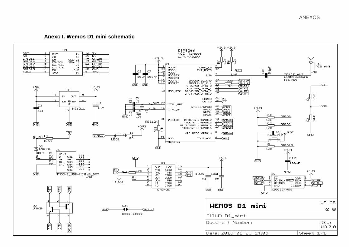
El esquema de la placa Wemos D1 mini se puede consultar en el .
Los datos y características del microcontrolador ESP8266EX se pueden
consultar en el .
Planta y vista inferior de la placa Wemos D1 mini.
Ilustración 4
Materiales INTRODUCCIÓN GENERAL
11
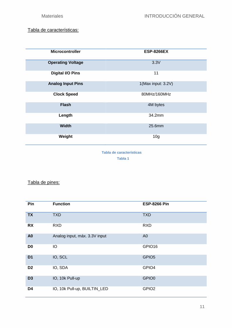
Tabla de características:
Microcontroller ESP-8266EX
Operating Voltage 3.3V
Digital I/O Pins 11
Analog Input Pins 1(Max input: 3.2V)
Clock Speed 80MHz/160MHz
Flash 4M bytes
Length 34.2mm
Width 25.6mm
Weight 10g
Tabla de características
Tabla 1
Tabla de pines:
Pin Function ESP-8266 Pin
TX TXD TXD
RX RXD RXD
A0 Analog input, máx. 3.3V input A0
D0 IO GPIO16
D1 IO, SCL GPIO5
D2 IO, SDA GPIO4
D3 IO, 10k Pull-up GPIO0
D4 IO, 10k Pull-up, BUILTIN_LED GPIO2
Materiales INTRODUCCIÓN GENERAL
12
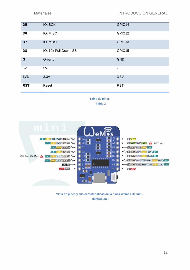
D5 IO, SCK GPIO14
D6 IO, MISO GPIO12
D7 IO, MOSI GPIO13
D8 IO, 10k Pull-Down, SS GPIO15
G Ground GND
5V 5V -
3V3 3.3V 3.3V
RST Reset RST
Tabla de pines
Tabla 2
Vista de pines y sus características de la placa Wemos D1 mini.
Ilustración 5
Materiales INTRODUCCIÓN GENERAL
13
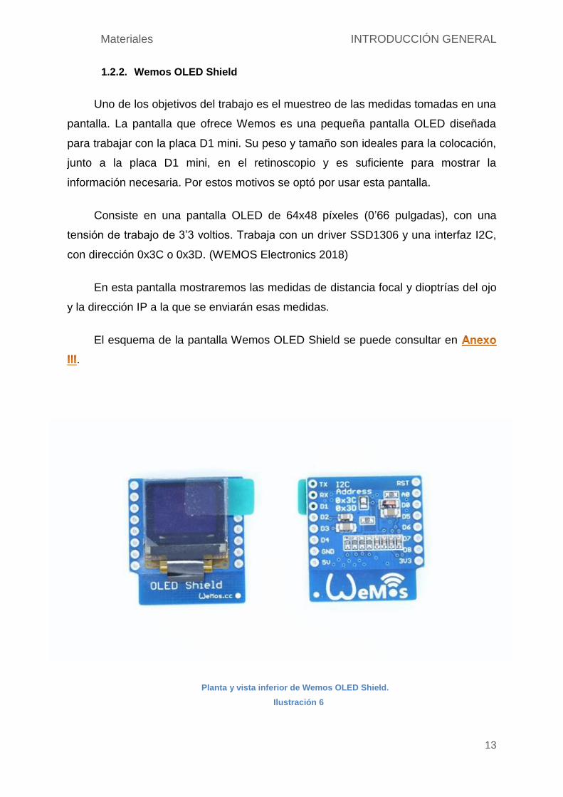
1.2.2. Wemos OLED Shield
Uno de los objetivos del trabajo es el muestreo de las medidas tomadas en una
pantalla. La pantalla que ofrece Wemos es una pequeña pantalla OLED diseñada
para trabajar con la placa D1 mini. Su peso y tamaño son ideales para la colocación,
junto a la placa D1 mini, en el retinoscopio y es suficiente para mostrar la
información necesaria. Por estos motivos se optó por usar esta pantalla.
Consiste en una pantalla OLED de 64x48 píxeles (0’66 pulgadas), con una
tensión de trabajo de 3’3 voltios. Trabaja con un driver SSD1306 y una interfaz I2C,
con dirección 0x3C o 0x3D. (WEMOS Electronics 2018)
En esta pantalla mostraremos las medidas de distancia focal y dioptrías del ojo
y la dirección IP a la que se enviarán esas medidas.
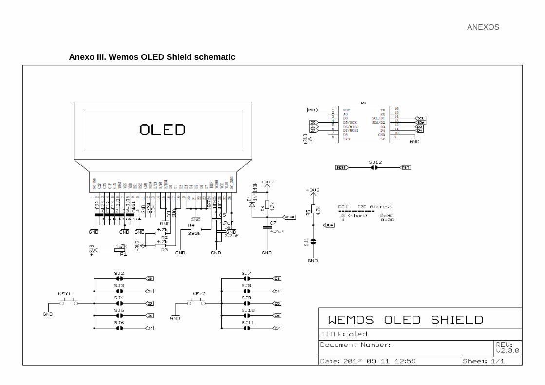
El esquema de la pantalla Wemos OLED Shield se puede consultar en
.
Planta y vista inferior de Wemos OLED Shield.
Ilustración 6
Materiales INTRODUCCIÓN GENERAL
14
1.2.3. Wemos Battery Shield
El retinoscopio manual funciona con dos pilas de tipo C de 1.5 V, lo que lo hace
totalmente manual e inalámbrico. El problema en el caso de este proyecto sería la
alimentación de la placa Wemos y sus componentes. Para ello, Wemos tiene un
componente en su catálogo con la capacidad de conectar una batería para alimentar
la placa y sus componentes, esa batería se puede recargar también gracias a dicho
componente.
Wemos Battery Shield se encargará de alimentar la placa Wemos D1 mini y
todos los componentes conectados a ella. Con una intensidad máxima de carga de 1
amperio y una tensión máxima de carga de 10 voltios, siendo 5 voltios la tensión de
carga recomendada.
El puerto de carga es un puerto micro USB y la batería irá conectada a un
puerto PH2-2.0MM.
Dispone de un LED rojo que lucirá cuando esté cagando y un LED verde
cuando ya esté cargado. (WEMOS Electronics 2017)
Este componente alimentará la placa con una batería conectada que podremos
cargar por la conexión micro-USB.
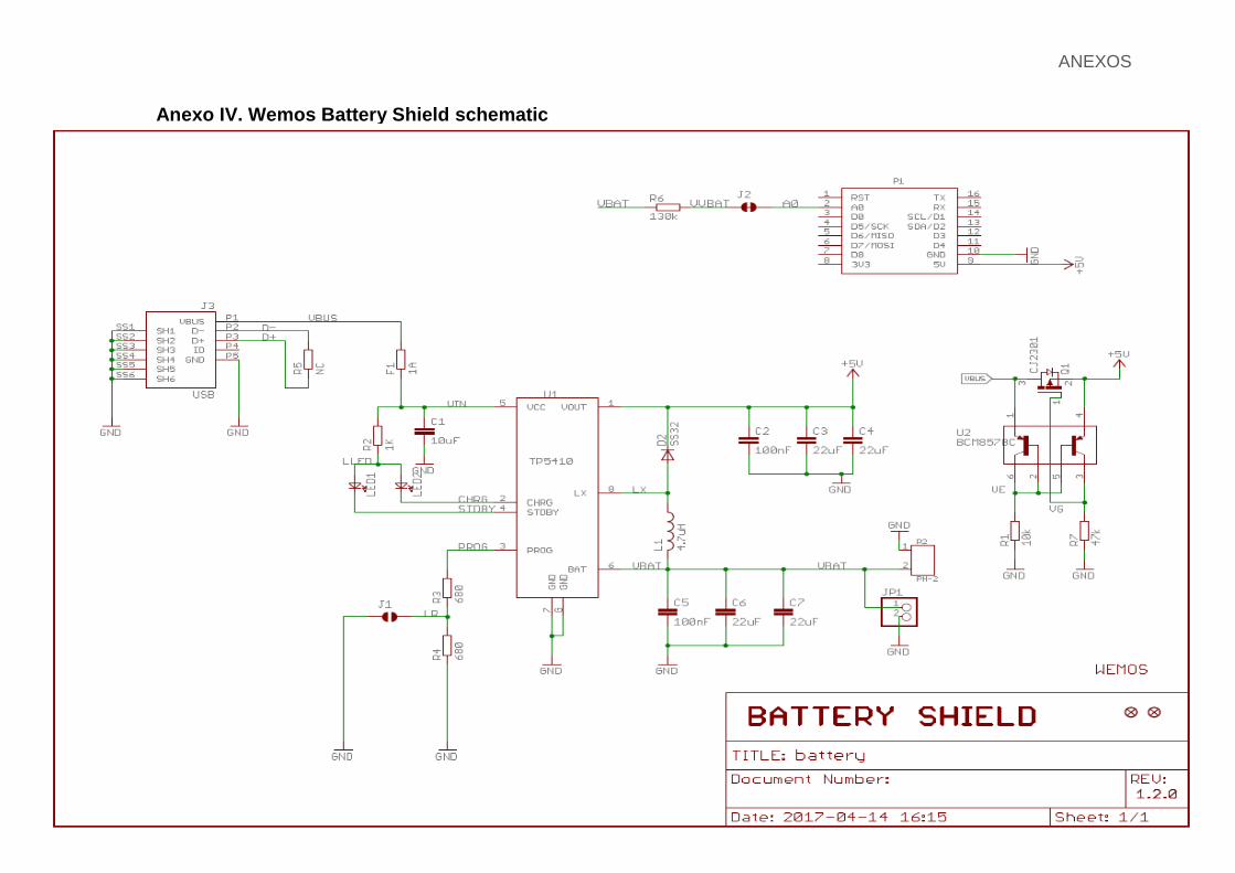
El esquema de Wemos Battery Shield se puede consultar en el .
Materiales INTRODUCCIÓN GENERAL
15
Planta de Wemos Battery Shield.
Ilustración 7
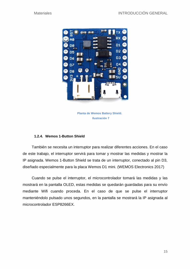
1.2.4. Wemos 1-Button Shield
También se necesita un interruptor para realizar diferentes acciones. En el caso
de este trabajo, el interruptor servirá para tomar y mostrar las medidas y mostrar la
IP asignada. Wemos 1-Button Shield se trata de un interruptor, conectado al pin D3,
diseñado especialmente para la placa Wemos D1 mini. (WEMOS Electronics 2017)
Cuando se pulse el interruptor, el microcontrolador tomará las medidas y las
mostrará en la pantalla OLED, estas medidas se quedarán guardadas para su envío
mediante Wifi cuando proceda. En el caso de que se pulse el interruptor
manteniéndolo pulsado unos segundos, en la pantalla se mostrará la IP asignada al
microcontrolador ESP8266EX.

Materiales INTRODUCCIÓN GENERAL
16
Planta de Wemos 1-Button Shield
Ilustración 8
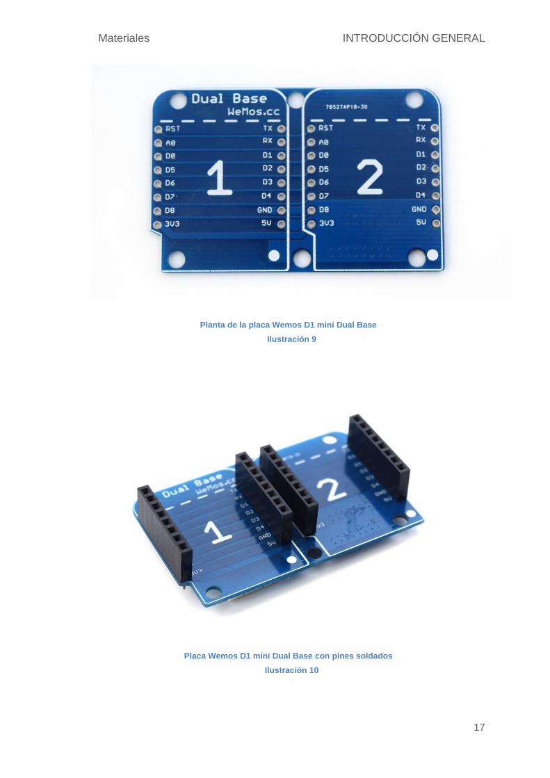
1.2.5. Wemos D1 Mini Dual Base Shield
Los componentes Shield de Wemos van montados, mediante pines y patillas
soldadas, uno sobre otro. Al tener varios componentes, para optimizar el espacio se
optó por usar la placa Wemos D1 Mini Dual Base Shield. Esta es una placa doble,
de 53 mm de largo y 34.2 mm de ancho, para mejorar la distribución de los
componentes.
Sobre esta base se distribuirán los componentes Shield de Wemos y la placa
Wemos D1 mini. Todos los componentes Wemos vienen con pines y patillas para
soldarlos a su placa.
Materiales INTRODUCCIÓN GENERAL
17
Planta de la placa Wemos D1 mini Dual Base
Ilustración 9
Placa Wemos D1 mini Dual Base con pines soldados
Ilustración 10
Materiales INTRODUCCIÓN GENERAL
18
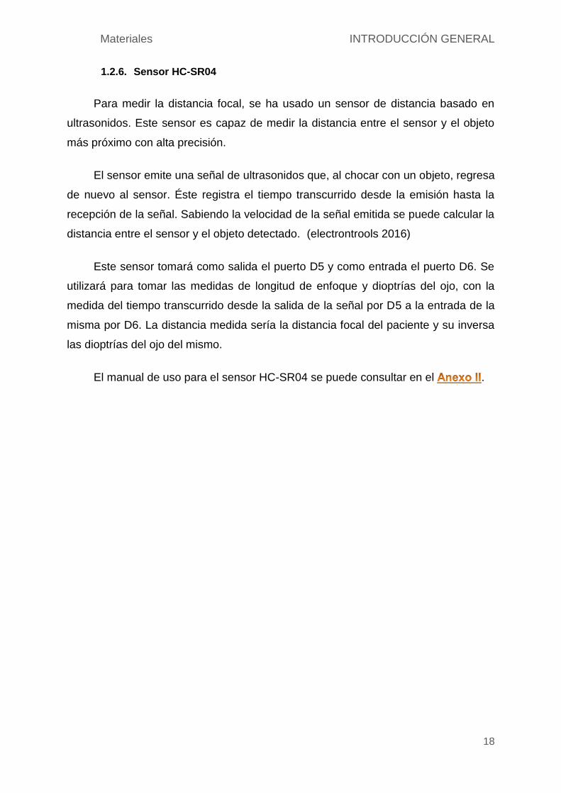
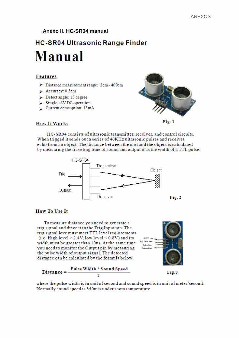
1.2.6. Sensor HC-SR04
Para medir la distancia focal, se ha usado un sensor de distancia basado en
ultrasonidos. Este sensor es capaz de medir la distancia entre el sensor y el objeto
más próximo con alta precisión.
El sensor emite una señal de ultrasonidos que, al chocar con un objeto, regresa
de nuevo al sensor. Éste registra el tiempo transcurrido desde la emisión hasta la
recepción de la señal. Sabiendo la velocidad de la señal emitida se puede calcular la
distancia entre el sensor y el objeto detectado. (electrontrools 2016)
Este sensor tomará como salida el puerto D5 y como entrada el puerto D6. Se
utilizará para tomar las medidas de longitud de enfoque y dioptrías del ojo, con la
medida del tiempo transcurrido desde la salida de la señal por D5 a la entrada de la
misma por D6. La distancia medida sería la distancia focal del paciente y su inversa
las dioptrías del ojo del mismo.
El manual de uso para el sensor HC-SR04 se puede consultar en el .
Materiales INTRODUCCIÓN GENERAL
19
Planta y vista inferior del sensor HC-SR04
Ilustración 11
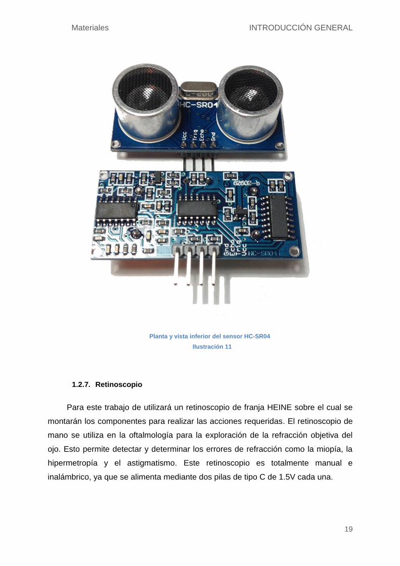
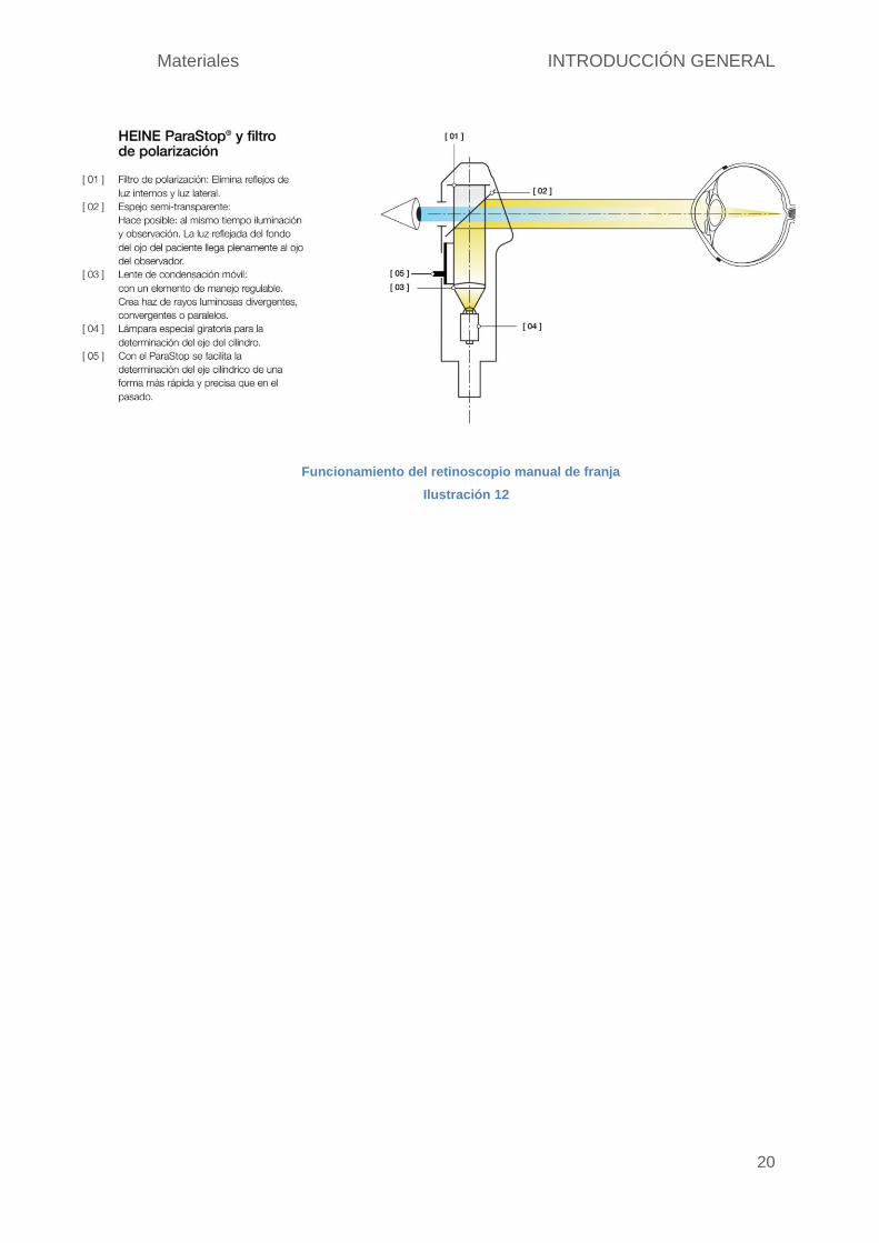
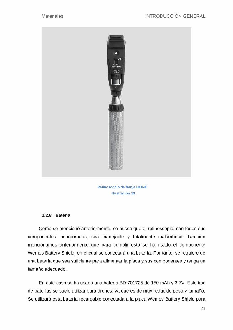
1.2.7. Retinoscopio
Para este trabajo de utilizará un retinoscopio de franja HEINE sobre el cual se
montarán los componentes para realizar las acciones requeridas. El retinoscopio de
mano se utiliza en la oftalmología para la exploración de la refracción objetiva del
ojo. Esto permite detectar y determinar los errores de refracción como la miopía, la
hipermetropía y el astigmatismo. Este retinoscopio es totalmente manual e
inalámbrico, ya que se alimenta mediante dos pilas de tipo C de 1.5V cada una.
Materiales INTRODUCCIÓN GENERAL
20
Funcionamiento del retinoscopio manual de franja
Ilustración 12
Materiales INTRODUCCIÓN GENERAL
21
Retinoscopio de franja HEINE
Ilustración 13
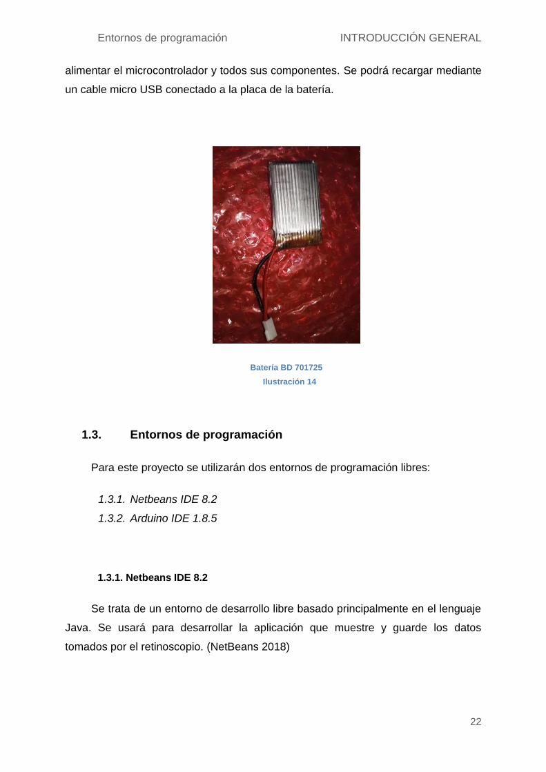
1.2.8. Batería
Como se mencionó anteriormente, se busca que el retinoscopio, con todos sus
componentes incorporados, sea manejable y totalmente inalámbrico. También
mencionamos anteriormente que para cumplir esto se ha usado el componente
Wemos Battery Shield, en el cual se conectará una batería. Por tanto, se requiere de
una batería que sea suficiente para alimentar la placa y sus componentes y tenga un
tamaño adecuado.
En este caso se ha usado una batería BD 701725 de 150 mAh y 3.7V. Este tipo
de baterías se suele utilizar para drones, ya que es de muy reducido peso y tamaño.
Se utilizará esta batería recargable conectada a la placa Wemos Battery Shield para
Entornos de programación INTRODUCCIÓN GENERAL
22
alimentar el microcontrolador y todos sus componentes. Se podrá recargar mediante
un cable micro USB conectado a la placa de la batería.
Batería BD 701725
Ilustración 14
1.3. Entornos de programación
Para este proyecto se utilizarán dos entornos de programación libres:
1.3.1. Netbeans IDE 8.2
1.3.2. Arduino IDE 1.8.5
1.3.1. Netbeans IDE 8.2
Se trata de un entorno de desarrollo libre basado principalmente en el lenguaje
Java. Se usará para desarrollar la aplicación que muestre y guarde los datos
tomados por el retinoscopio. (NetBeans 2018)

Entornos de programación INTRODUCCIÓN GENERAL
23
1.3.3. Arduino IDE 1.8.5
Arduino IDE es un software para microcontroladores basados en lenguaje C++.
Este entorno se usará para la programación del microcontrolador Wemos D1 mini.
(Arduino 2018)
METODOLOGÍA
2. METODOLOGÍA
El proyecto se realizó siguiendo los siguientes pasos:
Primero se realizó un estudio previo sobre el funcionamiento y características
de un retinoscopio manual, teniendo en cuenta las magnitudes a tratar durante el
trabajo. El motivo de este estudio es establecer el fin del proyecto y qué
componentes serán necesarios para llevarlo a cabo.
Con el objetivo ya definido, se procede a pedir los componentes y a obtener los
softwares necesarios para el trabajo. Se empieza a trabajar con el código que se
subirá a la placa Wemos D1 mini mediante el entorno de desarrollo Arduino IDE
1.8.5.
Cuando se obtuvieron todos los componentes se siguió trabajando con el
código incorporando las librerías y las líneas de código necesarias. Los
componentes, con las patillas debidamente soldadas, se van montando con la
distribución determinada, teniendo en cuenta la optimización del espacio y la utilidad
de cada componente.
Al terminar el código Arduino para la placa Wemos D1 mini y comprobar que
funciona correctamente, el último paso fue el desarrollo de la aplicación necesaria
para mostrar los datos en el ordenador y poder guardarlos en un archivo de texto.
Para ello, se trabajó con el entorno de desarrollo Netbeans IDE 8.2. Este sería el
último paso para completar los objetivos del proyecto.
Entornos de programación CONEXIONADO
25
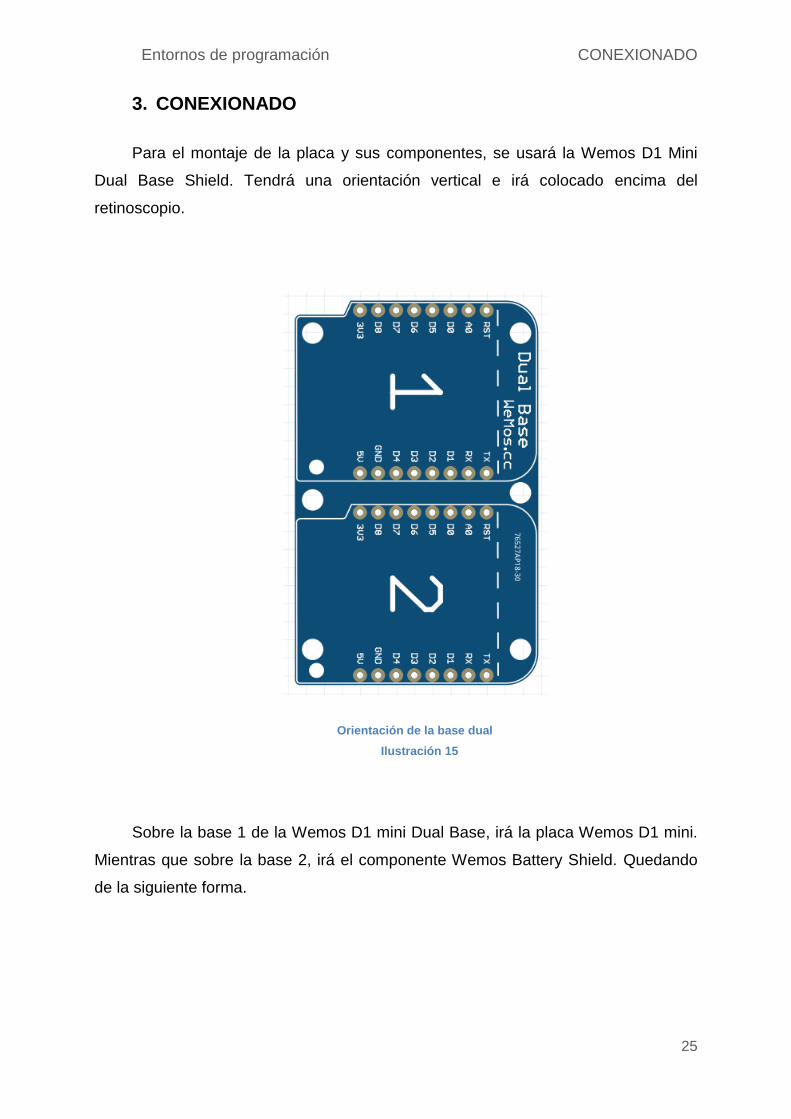
3. CONEXIONADO
Para el montaje de la placa y sus componentes, se usará la Wemos D1 Mini
Dual Base Shield. Tendrá una orientación vertical e irá colocado encima del
retinoscopio.
Orientación de la base dual
Ilustración 15
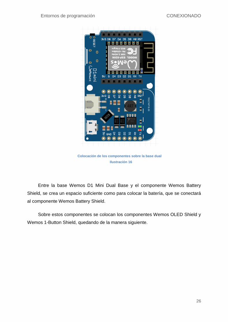
Sobre la base 1 de la Wemos D1 mini Dual Base, irá la placa Wemos D1 mini.
Mientras que sobre la base 2, irá el componente Wemos Battery Shield. Quedando
de la siguiente forma.
Entornos de programación CONEXIONADO
26
Colocación de los componentes sobre la base dual
Ilustración 16
Entre la base Wemos D1 Mini Dual Base y el componente Wemos Battery
Shield, se crea un espacio suficiente como para colocar la batería, que se conectará
al componente Wemos Battery Shield.
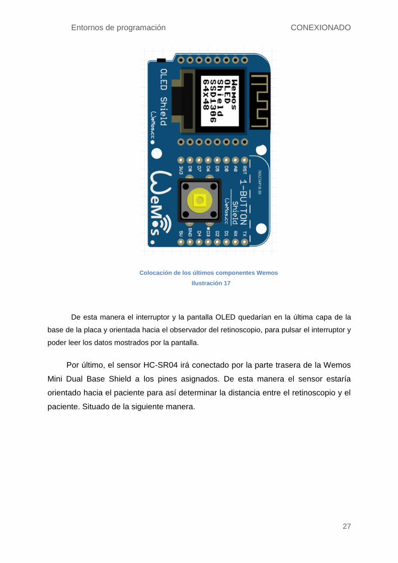
Sobre estos componentes se colocan los componentes Wemos OLED Shield y
Wemos 1-Button Shield, quedando de la manera siguiente.
Entornos de programación CONEXIONADO
27
Colocación de los últimos componentes Wemos
Ilustración 17
De esta manera el interruptor y la pantalla OLED quedarían en la última capa de la
base de la placa y orientada hacia el observador del retinoscopio, para pulsar el interruptor y
poder leer los datos mostrados por la pantalla.
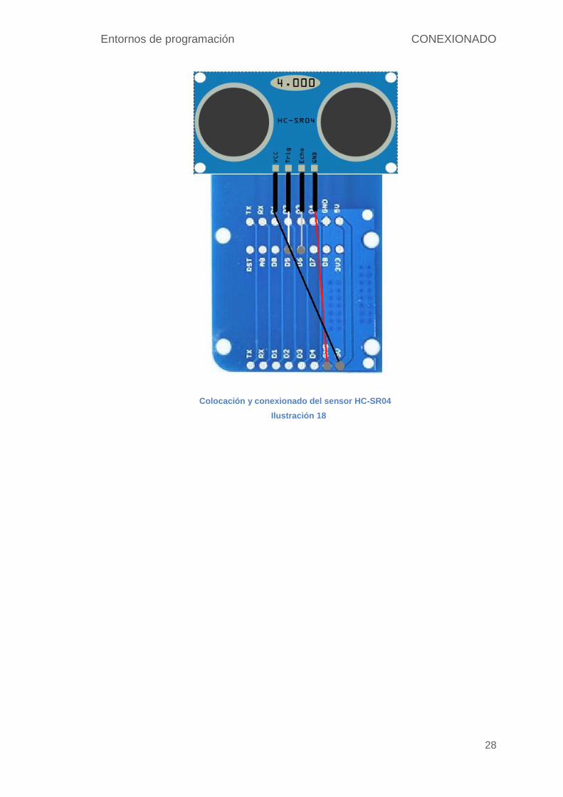
Por último, el sensor HC-SR04 irá conectado por la parte trasera de la Wemos
Mini Dual Base Shield a los pines asignados. De esta manera el sensor estaría
orientado hacia el paciente para así determinar la distancia entre el retinoscopio y el
paciente. Situado de la siguiente manera.
Entornos de programación CONEXIONADO
28
Colocación y conexionado del sensor HC-SR04
Ilustración 18
4.1. Configuración previa PROGRAMACIÓN DE ARDUINO IDE
29
4. PROGRAMACIÓN DE ARDUINO IDE
4.1. Configuración previa
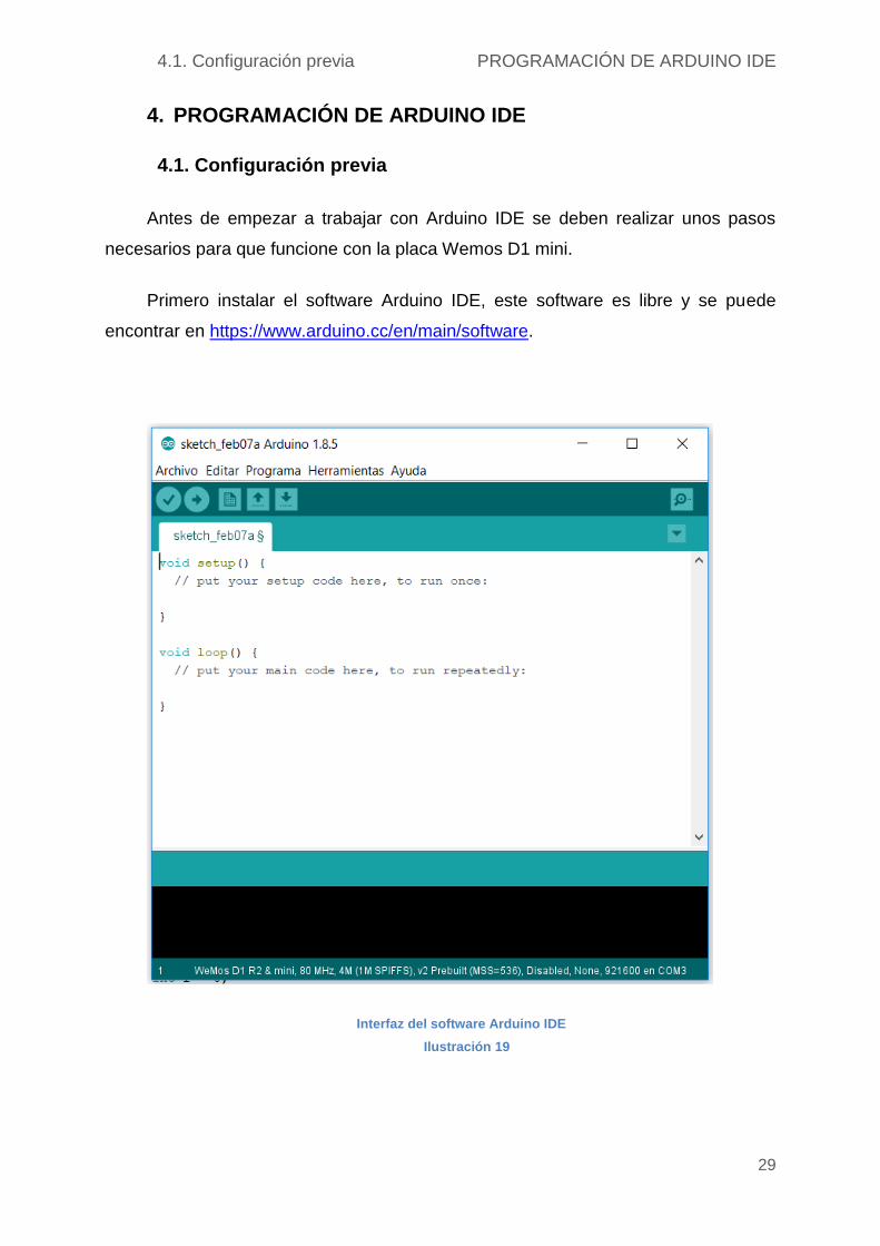
Antes de empezar a trabajar con Arduino IDE se deben realizar unos pasos
necesarios para que funcione con la placa Wemos D1 mini.
Primero instalar el software Arduino IDE, este software es libre y se puede
encontrar en https://www.arduino.cc/en/main/software.
Interfaz del software Arduino IDE
Ilustración 19
4.1. Configuración previa PROGRAMACIÓN DE ARDUINO IDE
30
Tras instalar el software, se procede a descargar el driver necesario para la
placa Wemos D1 mini, driver CH340G, que se puede encontrar en la página
https://wiki.wemos.cc/tutorials:get_started:get_started_in_arduino.
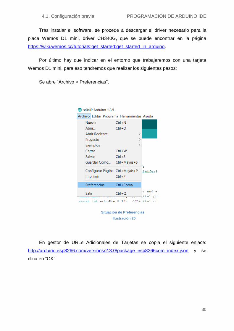
Por último hay que indicar en el entorno que trabajaremos con una tarjeta
Wemos D1 mini, para eso tendremos que realizar los siguientes pasos:
Se abre “Archivo > Preferencias”.
Situación de Preferencias
Ilustración 20
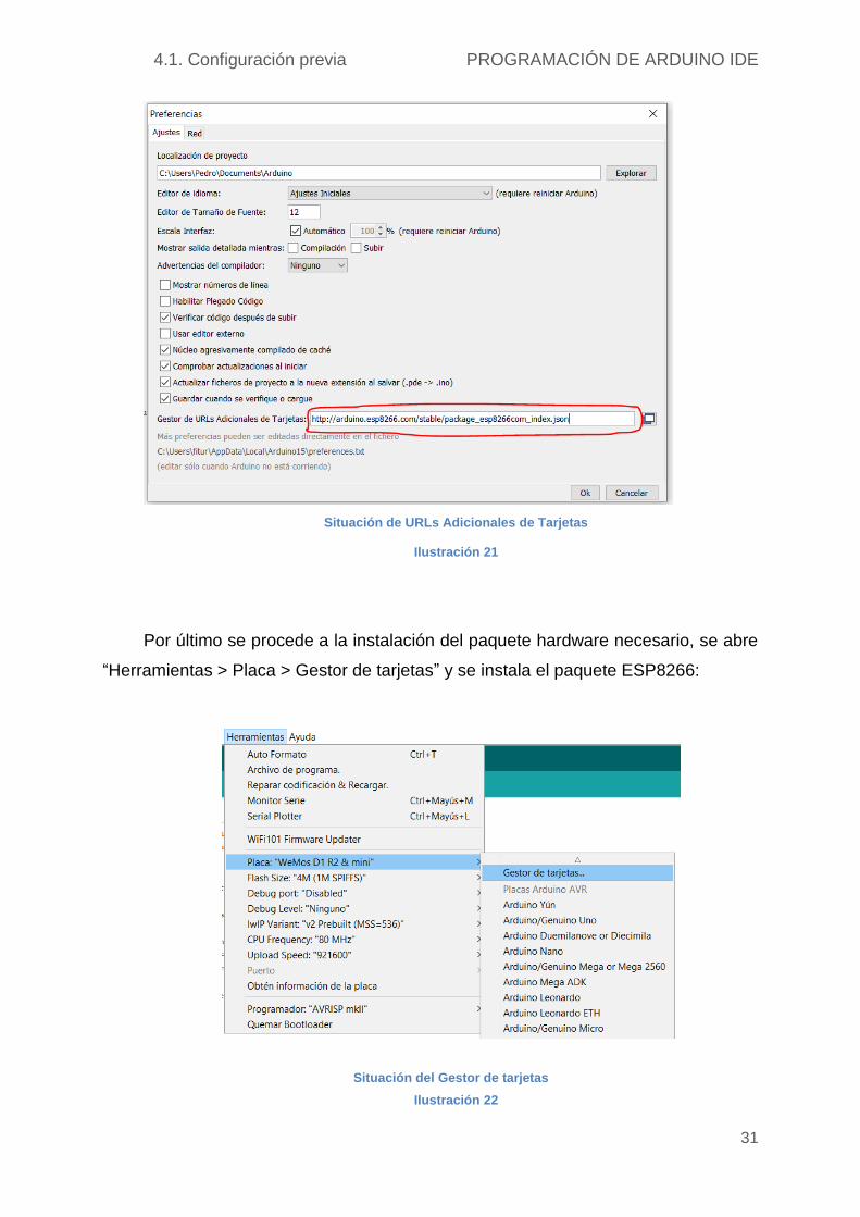
En gestor de URLs Adicionales de Tarjetas se copia el siguiente enlace:
http://arduino.esp8266.com/versions/2.3.0/package_esp8266com_index.json y se
clica en “OK”.
4.1. Configuración previa PROGRAMACIÓN DE ARDUINO IDE
31
Situación de URLs Adicionales de Tarjetas
Ilustración 21
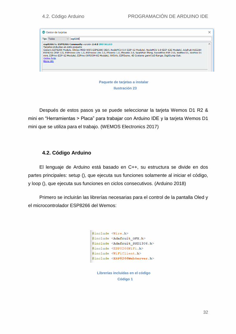
Por último se procede a la instalación del paquete hardware necesario, se abre
“Herramientas > Placa > Gestor de tarjetas” y se instala el paquete ESP8266:
Situación del Gestor de tarjetas
Ilustración 22
4.2. Código Arduino PROGRAMACIÓN DE ARDUINO IDE
32
Paquete de tarjetas a instalar
Ilustración 23
Después de estos pasos ya se puede seleccionar la tarjeta Wemos D1 R2 &
mini en “Herramientas > Placa” para trabajar con Arduino IDE y la tarjeta Wemos D1
mini que se utiliza para el trabajo. (WEMOS Electronics 2017)
4.2. Código Arduino
El lenguaje de Arduino está basado en C++, su estructura se divide en dos
partes principales: setup (), que ejecuta sus funciones solamente al iniciar el código,
y loop (), que ejecuta sus funciones en ciclos consecutivos. (Arduino 2018)
Primero se incluirán las librerías necesarias para el control de la pantalla Oled y
el microcontrolador ESP8266 del Wemos:
Librerías incluidas en el código
Código 1
4.2. Código Arduino PROGRAMACIÓN DE ARDUINO IDE
33
A continuación se define la configuración previa de la pantalla, los datos del
router Wifi y los pines y variables necesarios, también se creará el servidor web
donde se subirán los datos. En esta parte del código quedarán definidas las
constantes necesarias para el resto del código.
Parte del código anterior al setup ()
Código 2
Los pines trigPin y echoPin son los pines de emisión y recepción,
respectivamente, del sensor de ultrasonidos. El pin switchPin se trata del botón del
1-button Shield. El pin ledPin se refiere al led que lleva incorporado la placa D1 mini.
En el setup () se empieza configurando los pines como entrada o salida e
inicializando la pantalla Oled.
4.2. Código Arduino PROGRAMACIÓN DE ARDUINO IDE
34
Parte del setup () con la configuración previa de la pantalla y los pines
Código 3
La pantalla se configura con setRotation (3) para para que el texto se muestre
en la orientación necesaria para la posición de la pantalla en el retinoscopio. La
pantalla mostrará un saludo al encender el microcontrolador.
Siguiendo en el setup (), a continuación se inicia la conexión Wifi al router y se
arranca el servidor web.
4.2. Código Arduino PROGRAMACIÓN DE ARDUINO IDE
35
Resto del setup () con la conexión Wifi y arranque del servidor
Código 4
Se inicia la comunicación con el puerto serie y la conexión Wifi. Cuando se
realiza la conexión, la pantalla mostrará la IP que se le ha asignado, ésta será la IP
donde se enviarán los datos medidos.
Ya en el loop (), se realizan las acciones de consulta y llamadas a las funciones
necesarias.
4.2. Código Arduino PROGRAMACIÓN DE ARDUINO IDE
36
Contenido del loop ()
Código 5
server.handleClient () se activa al consultar externamente la IP del
microcontrolador y llama a la función webserver (), que se definirá más adelante.
Cuando se pulsa el interruptor, se llama a la función distanceData (), que se definirá
a continuación, y si el interruptor sigue pulsado unos segundos más, en la pantalla
se volverá a mostrar la IP para una nueva consulta. Si no se pulsa el interruptor
durante unos minutos la pantalla se apagará para ahorrar batería.
Una de las funciones que hemos usado en el loop () se trata de distanceData ()
cuyo código es el siguiente.
4.2. Código Arduino PROGRAMACIÓN DE ARDUINO IDE
37
Código de la función distanceData ()
Código 6
En esta función, se mide la distancia con el sensor de ultrasonidos y la fórmula
necesaria, se calcula las dioptrías con el dato anterior, se guardan esas medidas y
se muestran en la pantalla Oled.
Cuando se hace una consulta externa de la IP, ya sea desde la aplicación del
ordenador o por un navegador web, el código llama a la función webserver (), que
envía los datos guardados en la función anterior y los envía a esa IP. Esta función
tiene el siguiente código.
4.2. Código Arduino PROGRAMACIÓN DE ARDUINO IDE
38
Código de la función webserver ()
Código 7
Para mostrar la IP en la pantalla Oled, se utiliza la función displayIP (), cuyo
código sería el siguiente.
Código de la función displayIP ()
Código 8
De esta forma quedaría terminado el código de Arduino IDE, el
microcontrolador se conecta al ordenador mediante un cable adaptador micro USB –
USB, en el programa Arduino IDE, mediante Herramientas, se selecciona el puerto
donde se ha conectado el microcontrolador, y para acabar se clica en subir y, así,
quedaría cargado el programa en el microcontrolador.
5.1. Configuración previa PROGRAMACIÓN NETBEANS IDE
39
5. PROGRAMACIÓN NETBEANS IDE
5.1. Configuración previa
El entorno Netbeans IDE es de libre acceso desde su web oficial:
https://netbeans.org/features/index.html. Este entorno requiere la instalación de Java
JDK 7 o superior para su uso, éste se puede descargar e instalar gratuitamente
desde la web oficial: http://www.oracle.com/technetwork/java/javase/downloads/jdk8-
downloads-2133151.html. Java JDK es un paquete de desarrollo de Java para crear
aplicaciones con lenguaje Java. (NetBeans 2018)
Interfaz del software NetBeans IDE
Ilustración 24
5.2. Programación Netbeans IDE
El objetivo es hacer una aplicación que tome los datos enviados por el
microcontrolador los muestre y se puedan guardar en un archivo de texto. Para ello
se desarrolló una interfaz sencilla con dos campos de texto y tres botones.
5.2. Programación Netbeans IDE PROGRAMACIÓN NETBEANS IDE
40
Vista previa de la aplicación Java
Ilustración 25
Esta aplicación dispone de un campo de texto arriba con el texto “escriba aquí
la IP mostrada”, que se ha llamado en el código como JTextField1. En este campo
de texto el usuario debe escribir la IP a la que enviará los datos el microcontrolador,
dicha IP se mostrará en la pantalla Wemos OLED Shield de la placa.
También dispone de otro campo de texto más abajo de mayor tamaño que el
anterior, que se ha llamado en el código como JTextArea1, donde se mostrarán los
datos que suba el microcontrolador a la IP indicada. Estos datos se mostrarán al
pulsar el botón Actualizar, si se pulsa de nuevo los nuevos datos se escribirán en la
siguiente línea del campo de texto.
En cuanto a los botones, uno de ellos es el botón “Actualizar”, que al pulsarse
mostrará los datos enviados por el microcontrolador en el campo de texto
JTextArea1, definido anteriormente. Este botón contiene el siguiente código.
5.2. Programación Netbeans IDE PROGRAMACIÓN NETBEANS IDE
41
Código del botón Actualizar
Código 9
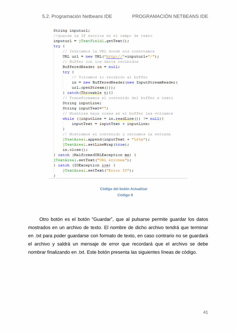
Otro botón es el botón “Guardar”, que al pulsarse permite guardar los datos
mostrados en un archivo de texto. El nombre de dicho archivo tendrá que terminar
en .txt para poder guardarse con formato de texto, en caso contrario no se guardará
el archivo y saldrá un mensaje de error que recordará que el archivo se debe
nombrar finalizando en .txt. Este botón presenta las siguientes líneas de código.
5.2. Programación Netbeans IDE PROGRAMACIÓN NETBEANS IDE
42
Código del botón Guardar
Código 10
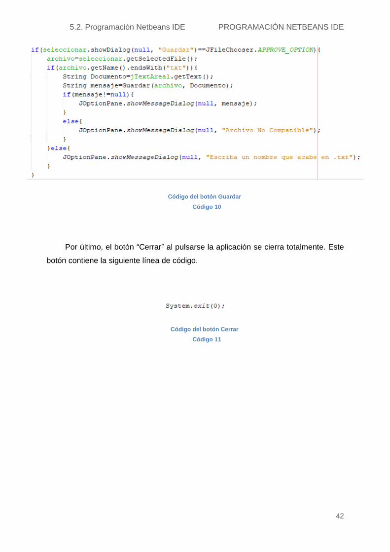
Por último, el botón “Cerrar” al pulsarse la aplicación se cierra totalmente. Este
botón contiene la siguiente línea de código.
Código del botón Cerrar
Código 11
5.3. Creación del ejecutable PROGRAMACIÓN NETBEANS IDE
43
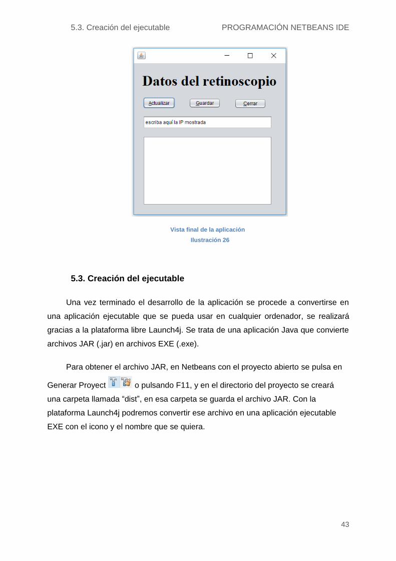
Vista final de la aplicación
Ilustración 26
5.3. Creación del ejecutable
Una vez terminado el desarrollo de la aplicación se procede a convertirse en
una aplicación ejecutable que se pueda usar en cualquier ordenador, se realizará
gracias a la plataforma libre Launch4j. Se trata de una aplicación Java que convierte
archivos JAR (.jar) en archivos EXE (.exe).
Para obtener el archivo JAR, en Netbeans con el proyecto abierto se pulsa en
Generar Proyect o pulsando F11, y en el directorio del proyecto se creará
una carpeta llamada “dist”, en esa carpeta se guarda el archivo JAR. Con la
plataforma Launch4j podremos convertir ese archivo en una aplicación ejecutable
EXE con el icono y el nombre que se quiera.
5.3. Creación del ejecutable PROGRAMACIÓN NETBEANS IDE
44
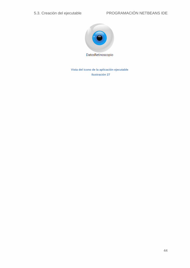
Vista del icono de la aplicación ejecutable
Ilustración 27
5.3. Creación del ejecutable PRESUPUESTO
45
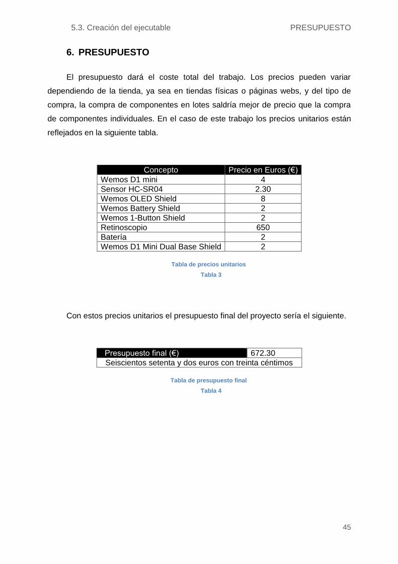
6. PRESUPUESTO
El presupuesto dará el coste total del trabajo. Los precios pueden variar
dependiendo de la tienda, ya sea en tiendas físicas o páginas webs, y del tipo de
compra, la compra de componentes en lotes saldría mejor de precio que la compra
de componentes individuales. En el caso de este trabajo los precios unitarios están
reflejados en la siguiente tabla.
Concepto Precio en Euros (€)
Wemos D1 mini 4
Sensor HC-SR04 2.30
Wemos OLED Shield 8
Wemos Battery Shield 2
Wemos 1-Button Shield 2
Retinoscopio 650
Batería 2
Wemos D1 Mini Dual Base Shield 2
Tabla de precios unitarios
Tabla 3
Con estos precios unitarios el presupuesto final del proyecto sería el siguiente.
Presupuesto final (€) 672.30
Seiscientos setenta y dos euros con treinta céntimos
Tabla de presupuesto final
Tabla 4
5.3. Creación del ejecutable CONCLUSIÓN
46
7. CONCLUSIÓN
Con la placa Wemos D1 mini, los componentes Wemos Shield necesarios y el
sensor de ultrasonidos HC-SR04, se ha conseguido cumplir con los objetivos del
proyecto.
Se buscaba un microcontrolador con conexión a red vía Wifi para la subida de
datos de manera inalámbrica. La placa Wemos D1 mini está basada en un
microcontrolador ESP8266EX, que dispone de conexión Wifi, y se puede programar
con Arduino IDE, un software basado en lenguaje C++ sencillo e intuitivo. También
dispone de componentes Shield que han sido de gran utilidad para el desarrollo del
proyecto. Con estas características y su reducido peso y tamaño, fue la placa ideal
para el proyecto.
Así, se consiguió que el retinoscopio con los componentes montados sea
manejable e inalámbrico, con un peso similar al retinoscopio sin los componentes y
sin cables que limiten su uso.
Con todos los componentes montados, el retinoscopio está listo para su uso.
Con el retinoscopio encendido, el observador hará una retinoscopía común para
determinar la distancia o longitud focal. El observador pulsará el interruptor para
tomar esa distancia con el sensor de ultrasonidos HC-SR04. De los datos del sensor
de ultrasonidos, se guardarán la distancia focal y las dioptrías del ojo, estos datos se
mostrarán en la pantalla.
En el ordenador podrá comprobar esos datos y guardarlos en un archivo de
texto con la aplicación creada con NetBeans llamada DatosRetinoscopio. Para ello,
sólo se necesita incluir la IP de la placa Wemos. Para conocer esa IP, se mostrará
en pantalla al inicio o manteniendo pulsado el interruptor durante varios segundos.
De esta manera quedaría definido el uso del retinoscopio con los componentes
montados, cumpliendo así los objetivos definidos al inicio del proyecto.
8. ANEXOS
ANEXOS
Anexo I. Wemos D1 mini schematic
ANEXOS
Anexo II. HC-SR04 manual
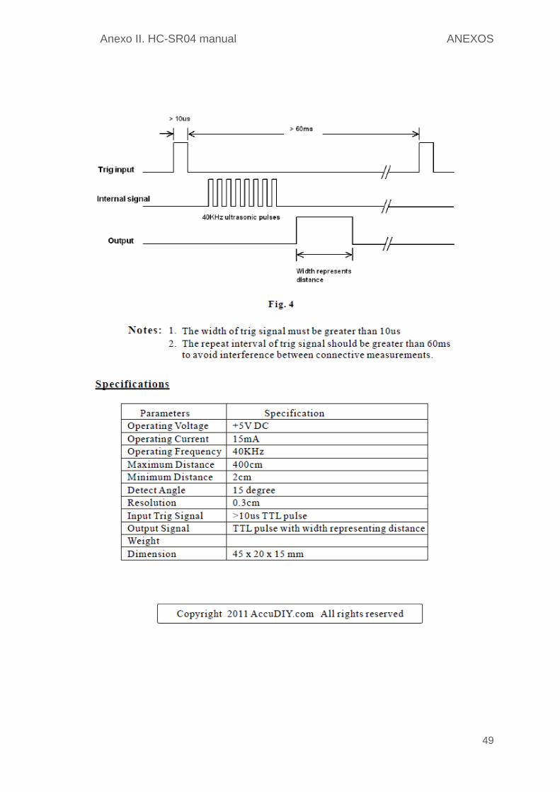
Anexo II. HC-SR04 manual ANEXOS
49
ANEXOS
Anexo III. Wemos OLED Shield schematic
ANEXOS
Anexo IV. Wemos Battery Shield schematic
Anexo V. ESP8266EX Datasheet ANEXOS
52
Anexo V. ESP8266EX Datasheet
ESP8266EX Datasheet Version 4.3
Espressif Systems IOT Team http://bbs.espressif.com/ Copyright © 2015

Disclaimer and Copyright Notice
Information in this document, including URL references, is subject to change without notice.
THIS DOCUMENT IS PROVIDED "AS IS" WITH NO WARRANTIES WHATSOEVER,
INCLUDING ANY WARRANTY OF MERCHANTABILITY, NON-INFRINGEMENT, FITNESS FOR
ANY PARTICULAR PURPOSE, OR ANY WARRANTY OTHERWISE ARISING OUT OF ANY
PROPOSAL, SPECIFICATION OR SAMPLE. All liability, including liability for infringement of
any proprietary rights, relating to use of information in this document is disclaimed. No
licenses express or implied, by estoppel or otherwise, to any intellectual property rights are
granted herein.
The Wi-Fi Alliance Member Logo is a trademark of the WiFi Alliance.
All trade names, trademarks and registered trademarks mentioned in this document are
property of their respective owners, and are hereby acknowledged.
Copyright © 2015 Espressif Systems. All rights reserved.
General Overview
Introduction
Espressif Systems’ Smart Connectivity Platform (ESCP) is a set of high performance, high integration
wireless SOCs, designed for space and power constrained mobile platform designers. It provides
unsurpassed ability to embed WiFi capabilities within other systems, or to function as a standalone
application, with the lowest cost, and minimal space requirement.
Figure 1 ESP8266EX Block Diagram
ESP8266EX offers a complete and self-contained WiFi networking solution; it can be used to host the
application or to offload WiFi networking functions from another application processor.
When ESP8266EX hosts the application, it boots up directly from an external flash. In has integrated
cache to improve the performance of the system in such applications.
Alternately, serving as a WiFi adapter, wireless internet access can be added to any micro controller-
based design with simple connectivity (SPI/SDIO or I2C/UART interface).
ESP8266EX is among the most integrated WiFi chip in the industry; it integrates the antenna
switches, RF balun, power amplifier, low noise receive amplifier, filters, power management modules, it
requires minimal external circuitry, and the entire solution, including front-end module, is designed to
occupy minimal PCB area.
ESP8266EX also integrates an enhanced version of Tensilica’s L106 Diamond series 32-bit processor,
with on-chip SRAM, besides the WiFi functionalities. ESP8266EX is often integrated with external
sensors and other application specific devices through its GPIOs; sample codes for such applications
are provided in the software development kit (SDK).
Espressif Systems’ Smart Connectivity Platform (ESCP) demonstrates sophisticated system-level
features include fast sleep/wake context switching for energy-efficient VoIP, adaptive radio biasing
for low-power operation, advance signal processing, and spur cancellation and radio co-existence
features for common cellular, Bluetooth, DDR, LVDS, LCD interference mitigation.
Features
• 802.11 b/g/n
• Integrated low power 32-bit MCU
• Integrated 10-bit ADC
• Integrated TCP/IP protocol stack
• Integrated TR switch, balun, LNA, power amplifier and matching network
• Integrated PLL, regulators, and power management units
• Supports antenna diversity
• WiFi 2.4 GHz, support WPA/WPA2
• Support STA/AP/STA+AP operation modes
• Support Smart Link Function for both Android and iOS devices
• SDIO 2.0, (H) SPI, UART, I2C, I2S, IR Remote Control, PWM, GPIO
• STBC, 1x1 MIMO, 2x1 MIMO
• A-MPDU & A-MSDU aggregation & 0.4s guard interval
• Deep sleep power <10uA, Power down leakage current < 5uA
• Wake up and transmit packets in < 2ms
• Standby power consumption of < 1.0mW (DTIM3)
• +20 dBm output power in 802.11b mode
• Operating temperature range -40C ~ 125C
• FCC, CE, TELEC, WiFi Alliance, and SRRC certified
Parameters
Table 1 Parameters
Categories Items Values
WiFi Paramters
Certificates FCC/CE/TELEC/SRRC
WiFi Protocles 802.11 b/g/n
Frequency Range 2.4G-2.5G (2400M-2483.5M)
Tx Power
802.11 b: +20 dBm
802.11 g: +17 dBm
802.11 n: +14 dBm
Rx Sensitivity
802.11 b: -91 dbm (11 Mbps)
802.11 g: -75 dbm (54 Mbps)
802.11 n: -72 dbm (MCS7)
Types of Antenna
PCB Trace, External, IPEX Connector,
Ceramic Chip
Hardware Paramaters
Peripheral Bus
UART/SDIO/SPI/I2C/I2S/IR Remote Control
GPIO/PWM
Operating Voltage 3.0~3.6V
Operating Current Average value: 80mA
Operating Temperature Range -40°~125°
Ambient Temperature Range Normal temperature
Package Size 5x5mm
External Interface N/A
Software
Parameters
WiFi mode station/softAP/SoftAP+station
Security WPA/WPA2
Encryption WEP/TKIP/AES
Firmware Upgrade UART Download / OTA (via network)
Ssoftware Development
Supports Cloud Server Development / SDK
for custom firmware development
Network Protocols IPv4, TCP/UDP/HTTP/FTP
User Configuration
AT Instruction Set, Cloud Server, Android/
iOS App
Ultra Low Power Technology
ESP8266EX has been designed for mobile, wearable electronics and Internet of Things applications
with the aim of achieving the lowest power consumption with a combination of several proprietary
techniques. The power saving architecture operates mainly in 3 modes: active mode, sleep mode
and deep sleep mode.
By using advance power management techniques and logic to power-down functions not required
and to control switching between sleep and active modes, ESP8266EX consumes about than 60uA in
deep sleep mode (with RTC clock still running) and less than 1.0mA (DTIM=3) or less than 0.5mA
(DTIM=10) to stay connected to the access point.
When in sleep mode, only the calibrated real-time clock and watchdog remains active. The real-time
clock can be programmed to wake up the ESP8266EX at any required interval.
The ESP8266EX can be programmed to wake up when a specified condition is detected. This
minimal wake-up time feature of the ESP8266EX can be utilized by mobile device SOCs, allowing
them to remain in the low-power standby mode until WiFi is needed.
In order to satisfy the power demand of mobile and wearable electronics, ESP8266EX can be
programmed to reduce the output power of the PA to fit various application profiles, by trading off
range for power consumption.
Major Applications
Major fields of ESP8266EX applications to Internet-of-Things include:
• Home Appliances
• Home Automation
• Smart Plug and lights
• Mesh Network
• Industrial Wireless Control
• Baby Monitors
• IP Cameras
• Sensor Networks
• Wearable Electronics

• WiFi Location-aware Devices
• Security ID Tags
• WiFi Position System Beacons

Hardware Overview
Pin Definitions
The pin assignments for 32-pin QFN package is illustrated in Fig.2.
Figure 2 Pin Assignments
Table 2 below presents an overview on the general pin attributes and the functions of each pin.
Table 2 Pin Definitions
Pin Name Type Function
1 VDDA P Analog Power 3.0 ~3.6V
2
LNA
I/O
RF Antenna Interface. Chip Output Impedance=50Ω
No matching required but we recommend that the π-type
matching network is retained.
3 VDD3P3 P Amplifier Power 3.0~3.6V
4 VDD3P3 P Amplifier Power 3.0~3.6V
5 VDD_RTC P NC (1.1V)
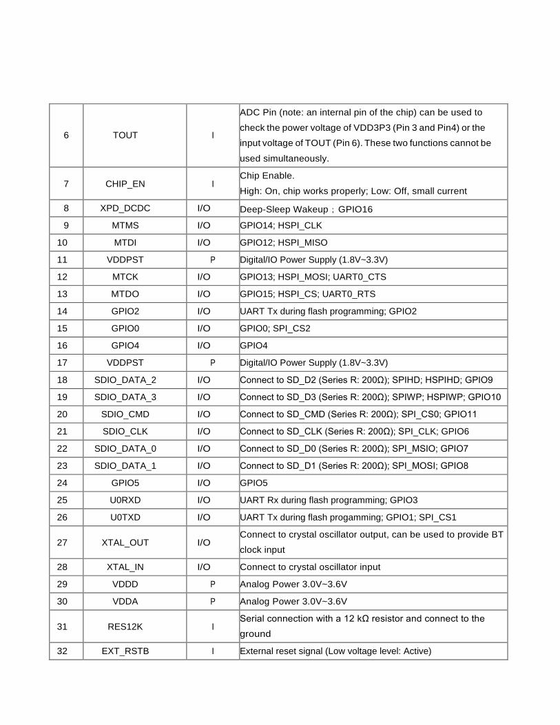
6
TOUT
I
ADC Pin (note: an internal pin of the chip) can be used to
check the power voltage of VDD3P3 (Pin 3 and Pin4) or the
input voltage of TOUT (Pin 6). These two functions cannot be
used simultaneously.
7
CHIP_EN
I Chip Enable.
High: On, chip works properly; Low: Off, small current
8 XPD_DCDC I/O Deep-Sleep Wakeup;GPIO16
9 MTMS I/O GPIO14; HSPI_CLK
10 MTDI I/O GPIO12; HSPI_MISO
11 VDDPST P Digital/IO Power Supply (1.8V~3.3V)
12 MTCK I/O GPIO13; HSPI_MOSI; UART0_CTS
13 MTDO I/O GPIO15; HSPI_CS; UART0_RTS
14 GPIO2 I/O UART Tx during flash programming; GPIO2
15 GPIO0 I/O GPIO0; SPI_CS2
16 GPIO4 I/O GPIO4
17 VDDPST P Digital/IO Power Supply (1.8V~3.3V)
18 SDIO_DATA_2 I/O Connect to SD_D2 (Series R: 200Ω); SPIHD; HSPIHD; GPIO9
19 SDIO_DATA_3 I/O Connect to SD_D3 (Series R: 200Ω); SPIWP; HSPIWP; GPIO10
20 SDIO_CMD I/O Connect to SD_CMD (Series R: 200Ω); SPI_CS0; GPIO11
21 SDIO_CLK I/O Connect to SD_CLK (Series R: 200Ω); SPI_CLK; GPIO6
22 SDIO_DATA_0 I/O Connect to SD_D0 (Series R: 200Ω); SPI_MSIO; GPIO7
23 SDIO_DATA_1 I/O Connect to SD_D1 (Series R: 200Ω); SPI_MOSI; GPIO8
24 GPIO5 I/O GPIO5
25 U0RXD I/O UART Rx during flash programming; GPIO3
26 U0TXD I/O UART Tx during flash progamming; GPIO1; SPI_CS1
27
XTAL_OUT
I/O Connect to crystal oscillator output, can be used to provide BT
clock input
28 XTAL_IN I/O Connect to crystal oscillator input
29 VDDD P Analog Power 3.0V~3.6V
30 VDDA P Analog Power 3.0V~3.6V
31
RES12K
I Serial connection with a 12 kΩ resistor and connect to the
ground
32 EXT_RSTB I External reset signal (Low voltage level: Active)
Note: GPIO2, GPIO0, MTDO can be configurable as 3-bit SDIO mode.
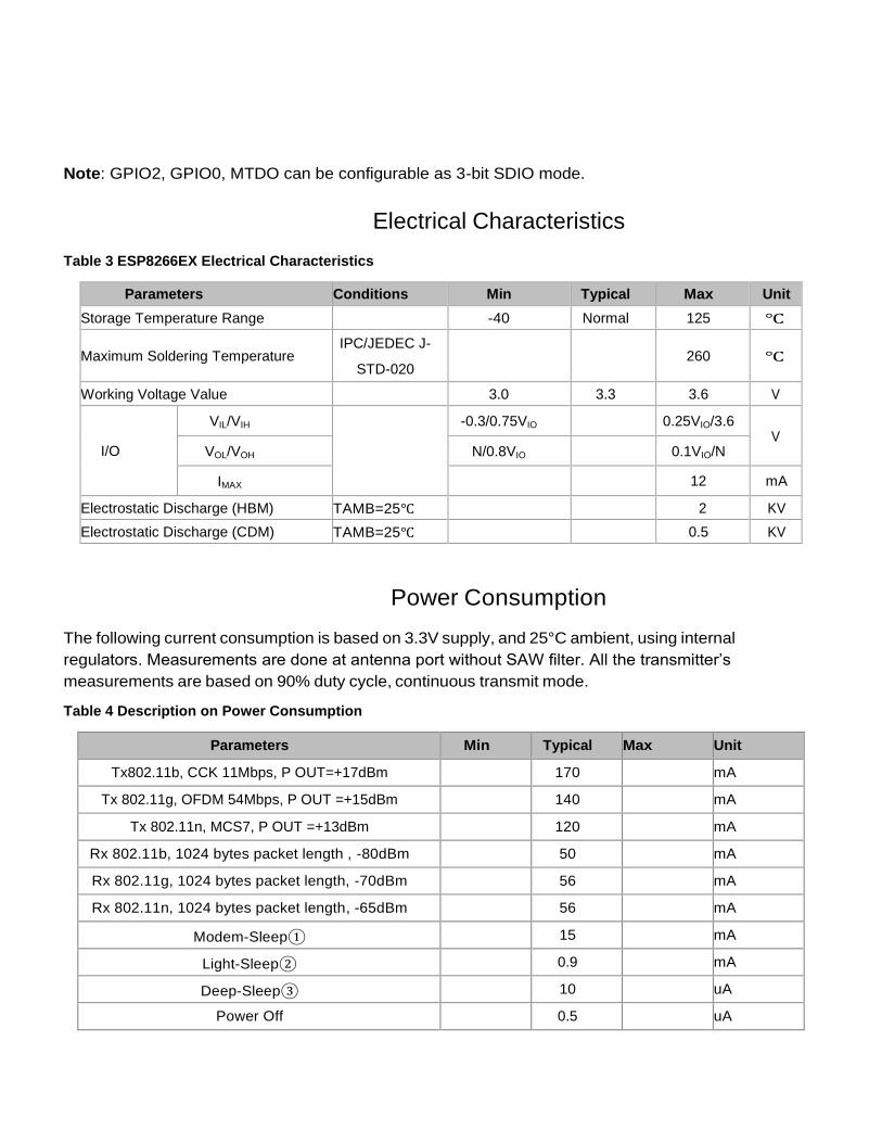
Electrical Characteristics
Table 3 ESP8266EX Electrical Characteristics
Parameters Conditions Min Typical Max Unit
Storage Temperature Range -40 Normal 125 ℃
Maximum Soldering Temperature
IPC/JEDEC J-
STD-020
260
℃
Working Voltage Value 3.0 3.3 3.6 V
I/O
VIL/VIH
-0.3/0.75VIO
0.25VIO/3.6 V
VOL/VOH N/0.8VIO
0.1VIO/N
IMAX 12 mA
Electrostatic Discharge (HBM) TAMB=25℃ 2 KV
Electrostatic Discharge (CDM) TAMB=25℃ 0.5 KV
Power Consumption
The following current consumption is based on 3.3V supply, and 25°C ambient, using internal
regulators. Measurements are done at antenna port without SAW filter. All the transmitter’s
measurements are based on 90% duty cycle, continuous transmit mode.
Table 4 Description on Power Consumption
Parameters Min Typical Max Unit
Tx802.11b, CCK 11Mbps, P OUT=+17dBm 170 mA
Tx 802.11g, OFDM 54Mbps, P OUT =+15dBm 140 mA
Tx 802.11n, MCS7, P OUT =+13dBm 120 mA
Rx 802.11b, 1024 bytes packet length , -80dBm 50 mA
Rx 802.11g, 1024 bytes packet length, -70dBm 56 mA
Rx 802.11n, 1024 bytes packet length, -65dBm 56 mA
Modem-Sleep① 15 mA
Light-Sleep② 0.9 mA
Deep-Sleep③ 10 uA
Power Off 0.5 uA
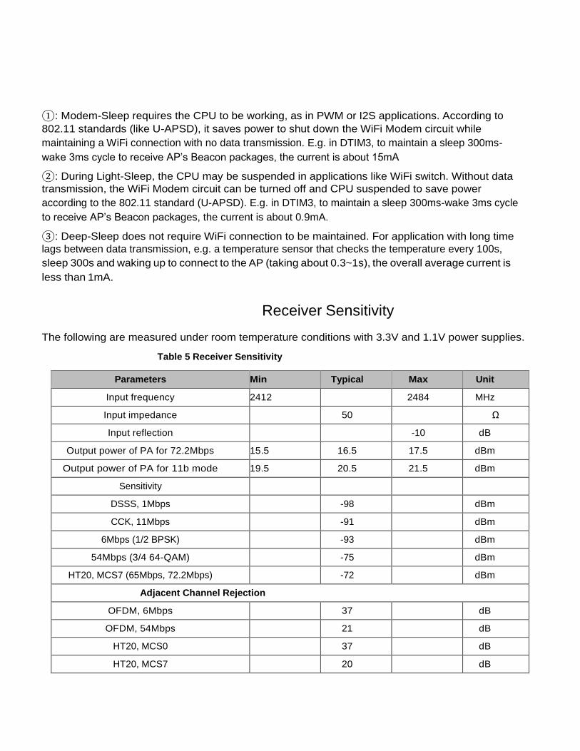
①: Modem-Sleep requires the CPU to be working, as in PWM or I2S applications. According to
802.11 standards (like U-APSD), it saves power to shut down the WiFi Modem circuit while
maintaining a WiFi connection with no data transmission. E.g. in DTIM3, to maintain a sleep 300ms-
wake 3ms cycle to receive AP’s Beacon packages, the current is about 15mA
②: During Light-Sleep, the CPU may be suspended in applications like WiFi switch. Without data
transmission, the WiFi Modem circuit can be turned off and CPU suspended to save power
according to the 802.11 standard (U-APSD). E.g. in DTIM3, to maintain a sleep 300ms-wake 3ms cycle
to receive AP’s Beacon packages, the current is about 0.9mA.
③: Deep-Sleep does not require WiFi connection to be maintained. For application with long time
lags between data transmission, e.g. a temperature sensor that checks the temperature every 100s,
sleep 300s and waking up to connect to the AP (taking about 0.3~1s), the overall average current is
less than 1mA.
Receiver Sensitivity
The following are measured under room temperature conditions with 3.3V and 1.1V power supplies.
Table 5 Receiver Sensitivity
Parameters Min Typical Max Unit
Input frequency 2412 2484 MHz
Input impedance 50 Ω
Input reflection -10 dB
Output power of PA for 72.2Mbps 15.5 16.5 17.5 dBm
Output power of PA for 11b mode 19.5 20.5 21.5 dBm
Sensitivity
DSSS, 1Mbps -98 dBm
CCK, 11Mbps -91 dBm
6Mbps (1/2 BPSK) -93 dBm
54Mbps (3/4 64-QAM) -75 dBm
HT20, MCS7 (65Mbps, 72.2Mbps) -72 dBm
Adjacent Channel Rejection
OFDM, 6Mbps 37 dB
OFDM, 54Mbps 21 dB
HT20, MCS0 37 dB
HT20, MCS7 20 dB
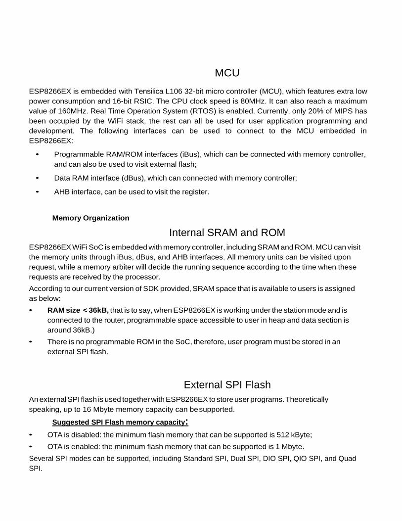
MCU
ESP8266EX is embedded with Tensilica L106 32-bit micro controller (MCU), which features extra low
power consumption and 16-bit RSIC. The CPU clock speed is 80MHz. It can also reach a maximum
value of 160MHz. Real Time Operation System (RTOS) is enabled. Currently, only 20% of MIPS has
been occupied by the WiFi stack, the rest can all be used for user application programming and
development. The following interfaces can be used to connect to the MCU embedded in
ESP8266EX:
• Programmable RAM/ROM interfaces (iBus), which can be connected with memory controller,
and can also be used to visit external flash;
• Data RAM interface (dBus), which can connected with memory controller;
• AHB interface, can be used to visit the register.
Memory Organization
Internal SRAM and ROM
ESP8266EX WiFi SoC is embedded with memory controller, including SRAM and ROM. MCU can visit
the memory units through iBus, dBus, and AHB interfaces. All memory units can be visited upon
request, while a memory arbiter will decide the running sequence according to the time when these
requests are received by the processor.
According to our current version of SDK provided, SRAM space that is available to users is assigned
as below:
• RAM size < 36kB, that is to say, when ESP8266EX is working under the station mode and is
connected to the router, programmable space accessible to user in heap and data section is
around 36kB.)
• There is no programmable ROM in the SoC, therefore, user program must be stored in an
external SPI flash.
External SPI Flash
An external SPI flash is used together with ESP8266EX to store user programs. Theoretically
speaking, up to 16 Mbyte memory capacity can be supported.
Suggested SPI Flash memory capacity:
• OTA is disabled: the minimum flash memory that can be supported is 512 kByte;
• OTA is enabled: the minimum flash memory that can be supported is 1 Mbyte.
Several SPI modes can be supported, including Standard SPI, Dual SPI, DIO SPI, QIO SPI, and Quad
SPI.

Therefore, please choose the correct SPI mode when you are downloading into the flash, otherwise
firmwares/programs that you downloaded may not work in the right way.
AHB and AHB Blocks
The AHB blocks performs the function of an arbiter, controls the AHB interfaces from the MAC, SDIO
(host) and CPU. Depending on the address, the AHB data requests can go into one of the two slaves:
APB block, or
flash controller (usually for standalone applications).
Data requests to the memory controller are usually high speed requests, and requests to the APB
block are usually register access.
The APB block acts as a decoder. It is meant only for access to programmable registers within
ESP8266’s main blocks. Depending on the address, the APB request can go to the radio, SI/SPI, SDIO
(host), GPIO, UART, real-time clock (RTC), MAC or digital baseband.
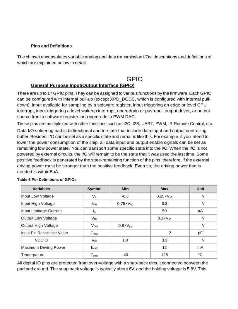
Pins and Definitions
The chipset encapsulates variable analog and data transmission I/Os, descriptions and definitions of
which are explained below in detail.
GPIO
General Purpose Input/Output Interface (GPIO)
There are up to 17 GPIO pins. They can be assigned to various functions by the firmware. Each GPIO
can be configured with internal pull-up (except XPD_DCDC, which is configured with internal pull-
down), input available for sampling by a software register, input triggering an edge or level CPU
interrupt, input triggering a level wakeup interrupt, open-drain or push-pull output driver, or output
source from a software register, or a sigma-delta PWM DAC.
These pins are multiplexed with other functions such as I2C, I2S, UART, PWM, IR Remote Control, etc.
Data I/O soldering pad is bidirectional and tri-state that include data input and output controlling
buffer. Besides, I/O can be set as a specific state and remains like this. For example, if you intend to
lower the power consumption of the chip, all data input and output enable signals can be set as
remaining low power state. You can transport some specific state into the I/O. When the I/O is not
powered by external circuits, the I/O will remain to be the state that it was used the last time. Some
positive feedback is generated by the state-remaining function of the pins, therefore, if the external
driving power must be stronger than the positive feedback. Even so, the driving power that is
needed is within 5uA.
Table 6 Pin Definitions of GPIOs
Variables Symbol Min Max Unit
Input Low Voltage VIL -0.3 0.25×VIO V
Input High Voltage VIH 0.75×VIO 3.3 V
Input Leakage Current IIL 50 nA
Output Low Voltage VOL 0.1×VIO V
Output High Voltage VOH 0.8×VIO V
Input Pin Resistance Value Cpad 2 pF
VDDIO VIO 1.8 3.3 V
Maximum Driving Power IMAX 12 mA
Temerpature Tamb -40 125 °C
All digital IO pins are protected from over-voltage with a snap-back circuit connected between the
pad and ground. The snap back voltage is typically about 6V, and the holding voltage is 5.8V. This
provides protection from over-voltages and ESD. The output devices are also protected from
reversed voltages with diodes.
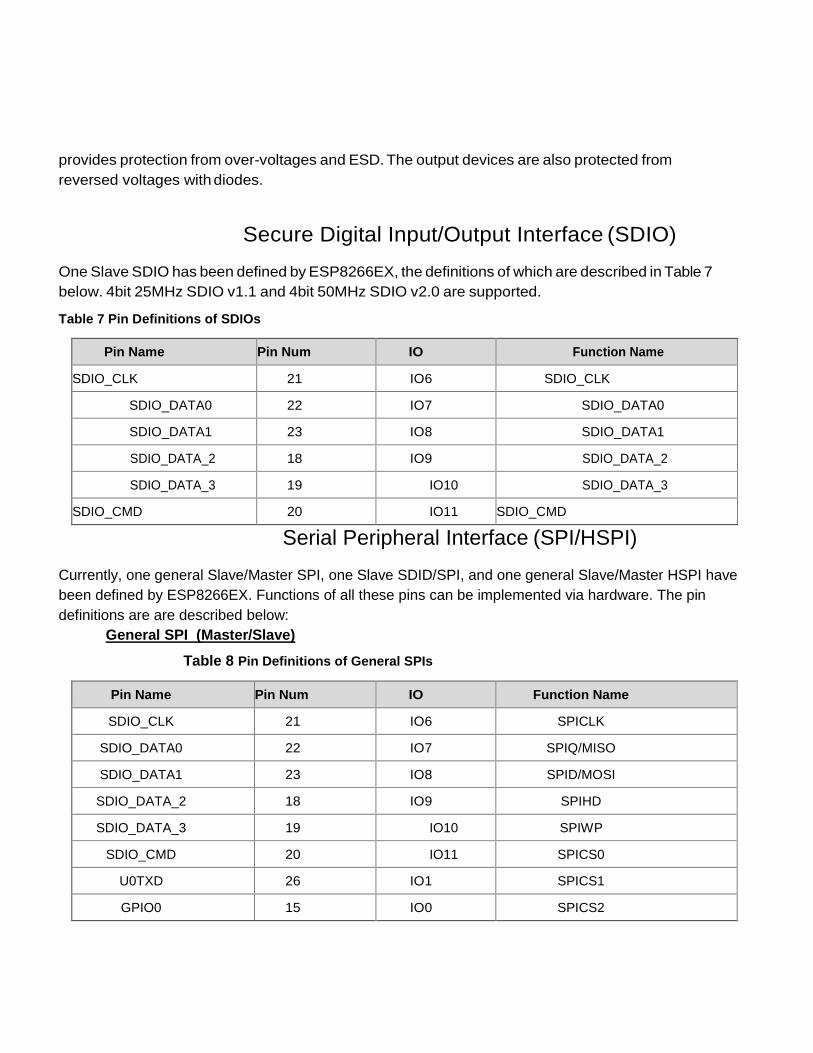
Secure Digital Input/Output Interface (SDIO)
One Slave SDIO has been defined by ESP8266EX, the definitions of which are described in Table 7
below. 4bit 25MHz SDIO v1.1 and 4bit 50MHz SDIO v2.0 are supported.
Table 7 Pin Definitions of SDIOs
Pin Name Pin Num IO Function Name
SDIO_CLK 21 IO6 SDIO_CLK
SDIO_DATA0 22 IO7 SDIO_DATA0
SDIO_DATA1 23 IO8 SDIO_DATA1
SDIO_DATA_2 18 IO9 SDIO_DATA_2
SDIO_DATA_3 19 IO10 SDIO_DATA_3
SDIO_CMD 20 IO11 SDIO_CMD
Serial Peripheral Interface (SPI/HSPI)
Currently, one general Slave/Master SPI, one Slave SDID/SPI, and one general Slave/Master HSPI have
been defined by ESP8266EX. Functions of all these pins can be implemented via hardware. The pin
definitions are are described below:
General SPI (Master/Slave)
Table 8 Pin Definitions of General SPIs
Pin Name Pin Num IO Function Name
SDIO_CLK 21 IO6 SPICLK
SDIO_DATA0 22 IO7 SPIQ/MISO
SDIO_DATA1 23 IO8 SPID/MOSI
SDIO_DATA_2 18 IO9 SPIHD
SDIO_DATA_3 19 IO10 SPIWP
SDIO_CMD 20 IO11 SPICS0
U0TXD 26 IO1 SPICS1
GPIO0 15 IO0 SPICS2
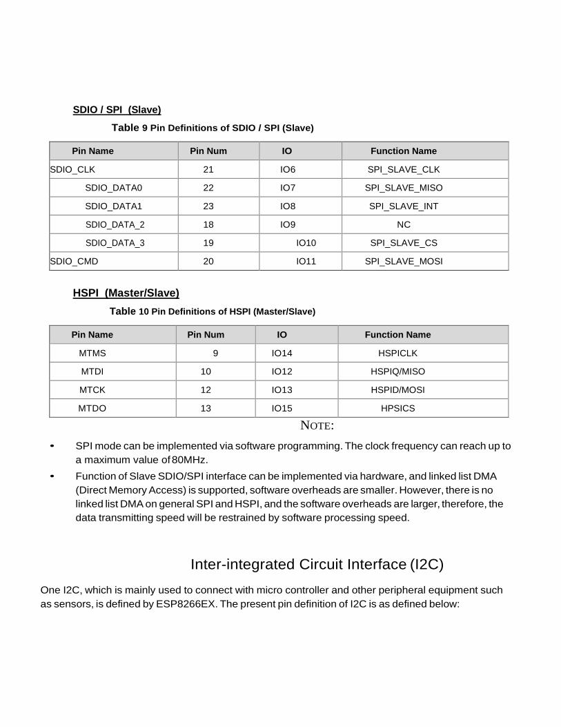
SDIO / SPI (Slave)
Table 9 Pin Definitions of SDIO / SPI (Slave)
Pin Name Pin Num IO Function Name
SDIO_CLK 21 IO6 SPI_SLAVE_CLK
SDIO_DATA0 22 IO7 SPI_SLAVE_MISO
SDIO_DATA1 23 IO8 SPI_SLAVE_INT
SDIO_DATA_2 18 IO9 NC
SDIO_DATA_3 19 IO10 SPI_SLAVE_CS
SDIO_CMD 20 IO11 SPI_SLAVE_MOSI
HSPI (Master/Slave)
Table 10 Pin Definitions of HSPI (Master/Slave)
Pin Name Pin Num IO Function Name
MTMS 9 IO14 HSPICLK
MTDI 10 IO12 HSPIQ/MISO
MTCK 12 IO13 HSPID/MOSI
MTDO 13 IO15 HPSICS
NOTE:
• SPI mode can be implemented via software programming. The clock frequency can reach up to
a maximum value of 80MHz.
• Function of Slave SDIO/SPI interface can be implemented via hardware, and linked list DMA
(Direct Memory Access) is supported, software overheads are smaller. However, there is no
linked list DMA on general SPI and HSPI, and the software overheads are larger, therefore, the
data transmitting speed will be restrained by software processing speed.
Inter-integrated Circuit Interface (I2C)
One I2C, which is mainly used to connect with micro controller and other peripheral equipment such
as sensors, is defined by ESP8266EX. The present pin definition of I2C is as defined below:
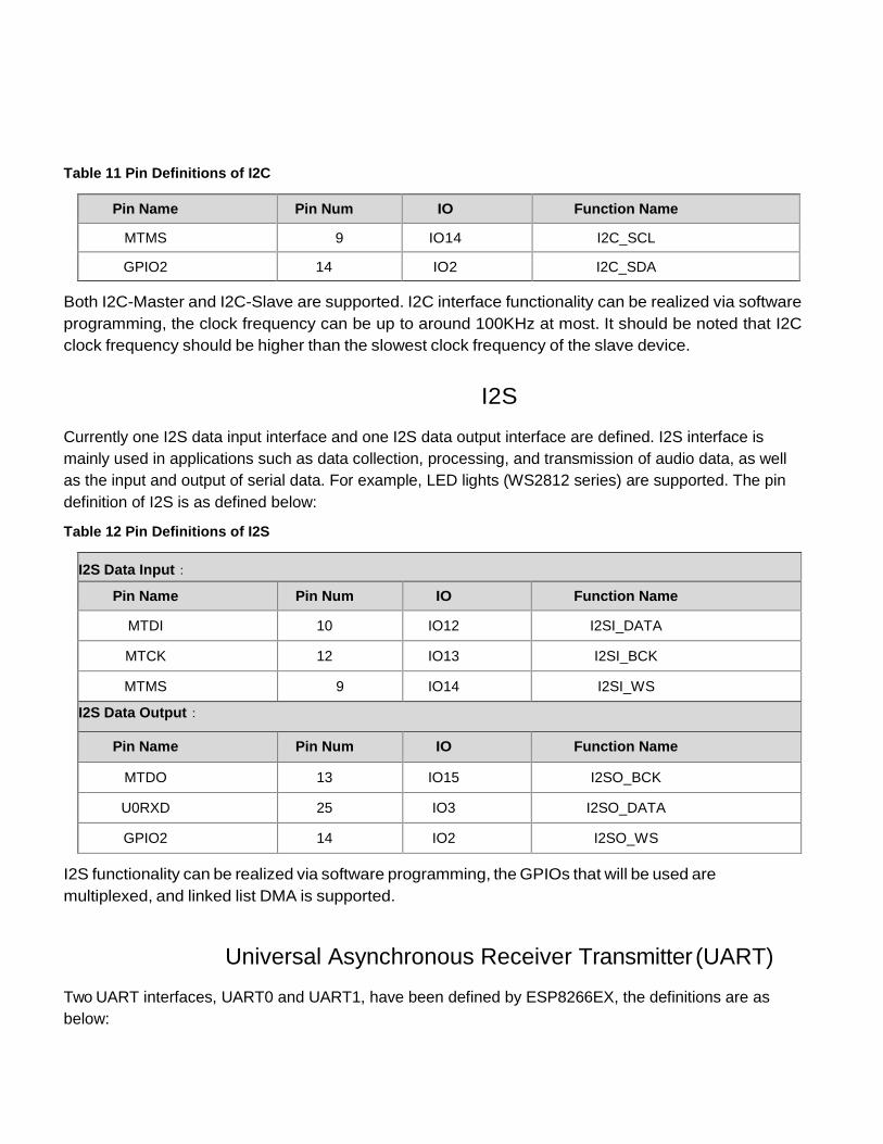
Table 11 Pin Definitions of I2C
Pin Name Pin Num IO Function Name
MTMS 9 IO14 I2C_SCL
GPIO2 14 IO2 I2C_SDA
Both I2C-Master and I2C-Slave are supported. I2C interface functionality can be realized via software
programming, the clock frequency can be up to around 100KHz at most. It should be noted that I2C
clock frequency should be higher than the slowest clock frequency of the slave device.
I2S
Currently one I2S data input interface and one I2S data output interface are defined. I2S interface is
mainly used in applications such as data collection, processing, and transmission of audio data, as well
as the input and output of serial data. For example, LED lights (WS2812 series) are supported. The pin
definition of I2S is as defined below:
Table 12 Pin Definitions of I2S
I2S Data Input:
Pin Name Pin Num IO Function Name
MTDI 10 IO12 I2SI_DATA
MTCK 12 IO13 I2SI_BCK
MTMS 9 IO14 I2SI_WS
I2S Data Output:
Pin Name Pin Num IO Function Name
MTDO 13 IO15 I2SO_BCK
U0RXD 25 IO3 I2SO_DATA
GPIO2 14 IO2 I2SO_WS
I2S functionality can be realized via software programming, the GPIOs that will be used are
multiplexed, and linked list DMA is supported.
Universal Asynchronous Receiver Transmitter (UART)
Two UART interfaces, UART0 and UART1, have been defined by ESP8266EX, the definitions are as
below:
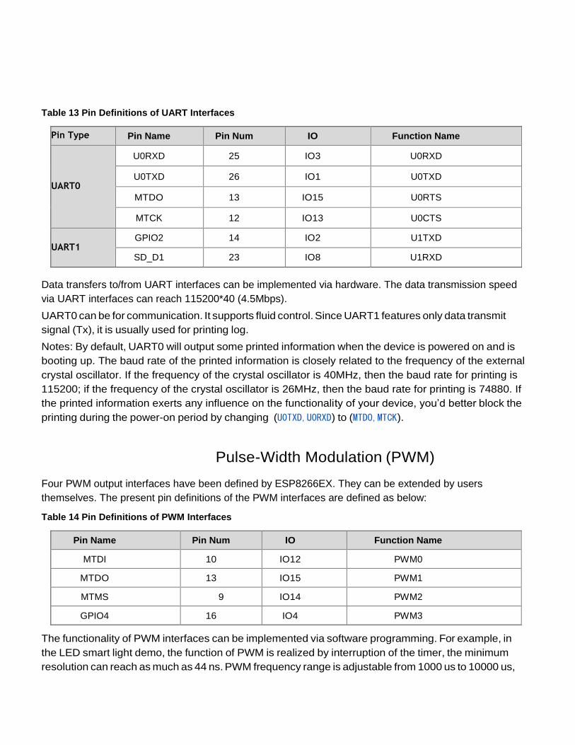
Table 13 Pin Definitions of UART Interfaces
Pin Type Pin Name Pin Num IO Function Name
UART0
U0RXD 25 IO3 U0RXD
U0TXD 26 IO1 U0TXD
MTDO 13 IO15 U0RTS
MTCK 12 IO13 U0CTS
UART1
GPIO2 14 IO2 U1TXD
SD_D1 23 IO8 U1RXD
Data transfers to/from UART interfaces can be implemented via hardware. The data transmission speed
via UART interfaces can reach 115200*40 (4.5Mbps).
UART0 can be for communication. It supports fluid control. Since UART1 features only data transmit
signal (Tx), it is usually used for printing log.
Notes: By default, UART0 will output some printed information when the device is powered on and is
booting up. The baud rate of the printed information is closely related to the frequency of the external
crystal oscillator. If the frequency of the crystal oscillator is 40MHz, then the baud rate for printing is
115200; if the frequency of the crystal oscillator is 26MHz, then the baud rate for printing is 74880. If
the printed information exerts any influence on the functionality of your device, you’d better block the
printing during the power-on period by changing (U0TXD,U0RXD) to (MTDO,MTCK).
Pulse-Width Modulation (PWM)
Four PWM output interfaces have been defined by ESP8266EX. They can be extended by users
themselves. The present pin definitions of the PWM interfaces are defined as below:
Table 14 Pin Definitions of PWM Interfaces
Pin Name Pin Num IO Function Name
MTDI 10 IO12 PWM0
MTDO 13 IO15 PWM1
MTMS 9 IO14 PWM2
GPIO4 16 IO4 PWM3
The functionality of PWM interfaces can be implemented via software programming. For example, in
the LED smart light demo, the function of PWM is realized by interruption of the timer, the minimum
resolution can reach as much as 44 ns. PWM frequency range is adjustable from 1000 us to 10000 us,
i.e., between 100Hz and 1KHz. When the PWM frequency is at 1 KHz, the duty ratio will reach
1/22727, and over 14 bit resolution will be achieved at 1KHz refresh rate.
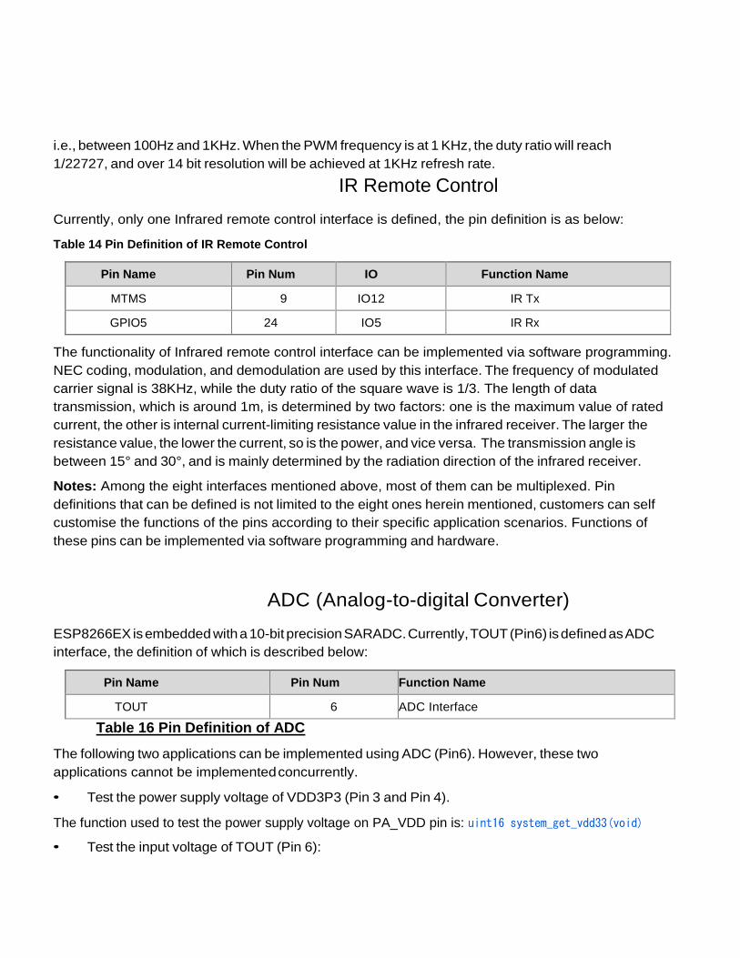
IR Remote Control
Currently, only one Infrared remote control interface is defined, the pin definition is as below:
Table 14 Pin Definition of IR Remote Control
Pin Name Pin Num IO Function Name
MTMS 9 IO12 IR Tx
GPIO5 24 IO5 IR Rx
The functionality of Infrared remote control interface can be implemented via software programming.
NEC coding, modulation, and demodulation are used by this interface. The frequency of modulated
carrier signal is 38KHz, while the duty ratio of the square wave is 1/3. The length of data
transmission, which is around 1m, is determined by two factors: one is the maximum value of rated
current, the other is internal current-limiting resistance value in the infrared receiver. The larger the
resistance value, the lower the current, so is the power, and vice versa. The transmission angle is
between 15° and 30°, and is mainly determined by the radiation direction of the infrared receiver.
Notes: Among the eight interfaces mentioned above, most of them can be multiplexed. Pin
definitions that can be defined is not limited to the eight ones herein mentioned, customers can self
customise the functions of the pins according to their specific application scenarios. Functions of
these pins can be implemented via software programming and hardware.
ADC (Analog-to-digital Converter)
ESP8266EX is embedded with a 10-bit precision SARADC. Currently, TOUT (Pin6) is defined as ADC
interface, the definition of which is described below:
Pin Name Pin Num Function Name
TOUT 6 ADC Interface
Table 16 Pin Definition of ADC
The following two applications can be implemented using ADC (Pin6). However, these two
applications cannot be implemented concurrently.
• Test the power supply voltage of VDD3P3 (Pin 3 and Pin 4).
The function used to test the power supply voltage on PA_VDD pin is: uint16 system_get_vdd33(void)
• Test the input voltage of TOUT (Pin 6):
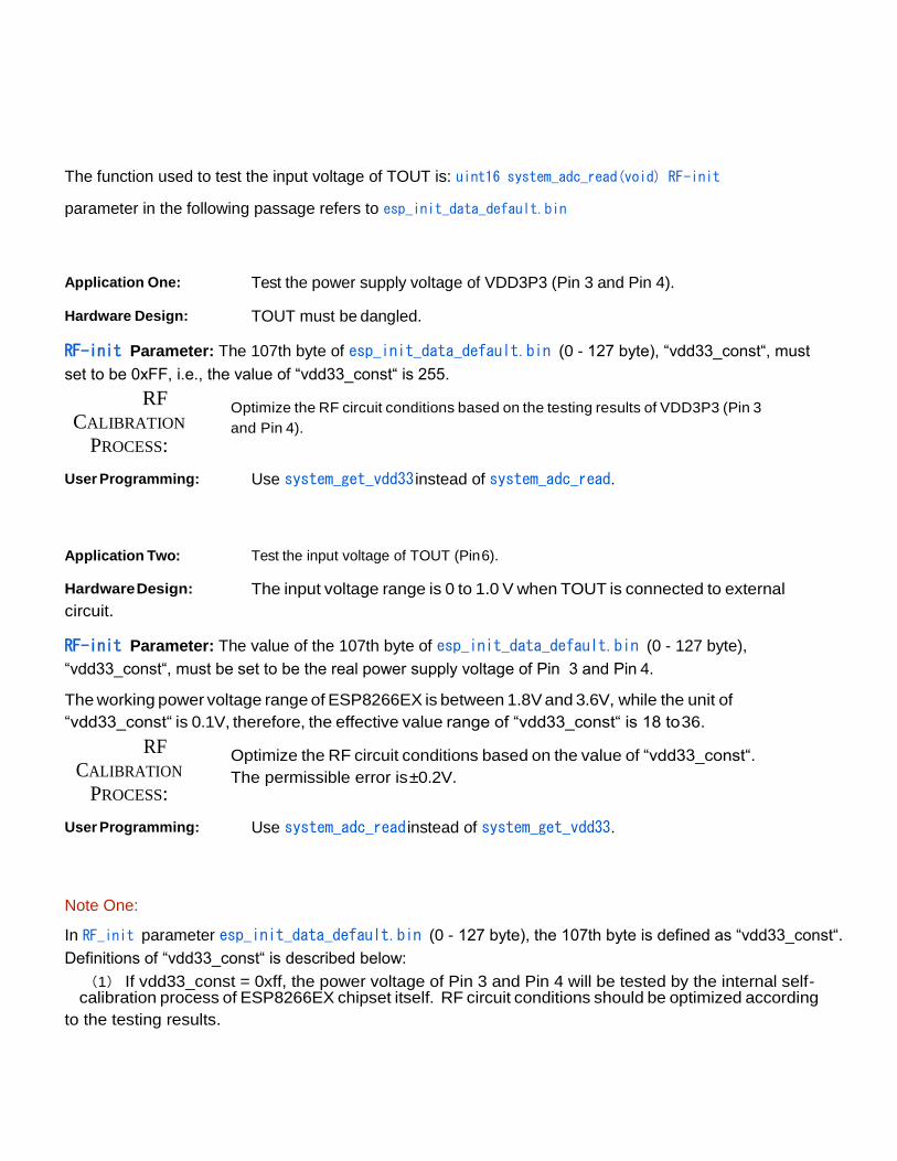
The function used to test the input voltage of TOUT is: uint16 system_adc_read(void) RF-init
parameter in the following passage refers to esp_init_data_default.bin
Application One: Test the power supply voltage of VDD3P3 (Pin 3 and Pin 4).
Hardware Design: TOUT must be dangled.
RF-init Parameter: The 107th byte of esp_init_data_default.bin (0 - 127 byte), “vdd33_const“, must
set to be 0xFF, i.e., the value of “vdd33_const“ is 255.
RF
CALIBRATION
PROCESS:
Optimize the RF circuit conditions based on the testing results of VDD3P3 (Pin 3
and Pin 4).
User Programming: Use system_get_vdd33 instead of system_adc_read.
Application Two: Test the input voltage of TOUT (Pin 6).
Hardware Design: The input voltage range is 0 to 1.0 V when TOUT is connected to external
circuit.
RF-init Parameter: The value of the 107th byte of esp_init_data_default.bin (0 - 127 byte),
“vdd33_const“, must be set to be the real power supply voltage of Pin 3 and Pin 4.
The working power voltage range of ESP8266EX is between 1.8V and 3.6V, while the unit of
“vdd33_const“ is 0.1V, therefore, the effective value range of “vdd33_const“ is 18 to 36.
RF
CALIBRATION
PROCESS:
Optimize the RF circuit conditions based on the value of “vdd33_const“.
The permissible error is ±0.2V.
User Programming: Use system_adc_read instead of system_get_vdd33.
Note One:
In RF_init parameter esp_init_data_default.bin (0 - 127 byte), the 107th byte is defined as “vdd33_const“.
Definitions of “vdd33_const“ is described below:
(1) If vdd33_const = 0xff, the power voltage of Pin 3 and Pin 4 will be tested by the internal self- calibration process of ESP8266EX chipset itself. RF circuit conditions should be optimized according
to the testing results.
(2) If 18 =< vdd33_const =< 36, ESP8266EX RF Calibration and optimization process is implemented via (vdd33_const/10).
(3) If vdd33_const < 18 or 36 < vdd33_const < 255, ESP8266EX RF Calibration and optimization process is implemented via the default value 3.0V.
Note Two:
Function system_get_vdd33 is used to test the power supply voltage of VDD3P3 (Pin 3 and Pin 4). Details
on this function are described below:
(1) Pin Tout must be dangled. The 107th byte of esp_init_data_default.bin (0 - 127 byte), “vdd33_const“, must set to be 0xFF.
(2) If the 107th byte of esp_init_data_default.bin (0 - 127 byte), “vdd33_const“, is equal to
0xff, the returned value of function system_get_vdd33 will be an effective value, otherwise 0xffff
will be returned.
(3) The unit of the returned value is: 1/1024 V.
Note Three:
Function system_adc_read is defined to test the input voltage of Pin TOUT (Pin 6). Details on this
function are described below:
(1) The value of the 107th byte of esp_init_data_default.bin (0 - 127 byte), “vdd33_const“, must be set to be the real power supply voltage of Pin 3 and Pin 4.
(2) If the 107th byte of esp_init_data_default.bin (0 - 127 byte), “vdd33_const“, is NOT equal to 0xff, the returned value of system_adc_read will be an effective value of the input voltage
of Pin TOUT, otherwise 0xffff will be returned.
(3) The unit of the returned value is: 1/1024 V.
LED Light and Button
ESP8266EX features up to 17 GPIOs, all of which can be assigned to realise various functions of LED
lights and buttons. Definitions of some GPIOs that are assigned with certain functions in our demo
application design are shown below:
Table 17 Pin Definitions of LED and Button
Pin Name Pin Num IO Function Name
MTCK 12 IO13 Button (Reset)
GPIO0 15 IO0 WiFi Light
MTDI 10 IO12 Link Light
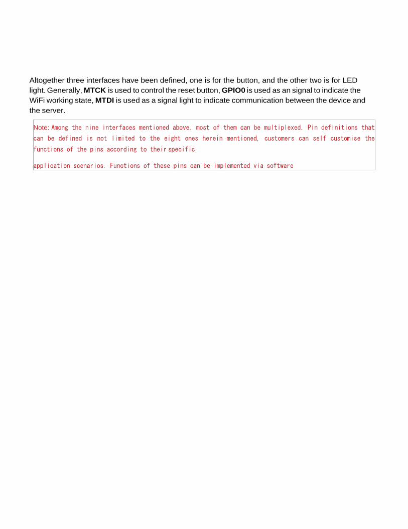
Note: Among the nine interfaces mentioned above, most of them can be multiplexed. Pin definitions that
can be defined is not limited to the eight ones herein mentioned, customers can self customise the
functions of the pins according to their specific
application scenarios. Functions of these pins can be implemented via software
programming and hardware.
Altogether three interfaces have been defined, one is for the button, and the other two is for LED
light. Generally, MTCK is used to control the reset button, GPIO0 is used as an signal to indicate the
WiFi working state, MTDI is used as a signal light to indicate communication between the device and
the server.
Firmware & Software Development Kit
The application and firmware is executed in on-chip ROM and SRAM, which loads the instructions
during wake-up, through the SDIO interface, from the external flash.
The firmware implements TCP/IP, the full 802.11 b/g/n/e/i WLAN MAC protocol and WiFi Direct
specification. It supports not only basic service set (BSS) operations under the distributed control
function (DCF) but also P2P group operation compliant with the latest WiFi P2P protocol. Low level
protocol functions are handled automatically by ESP8266:
• RTS/CTS
• acknowledgement
• fragmentation and defragmentation
• aggregation
• frame encapsulation (802.11h/RFC 1042)
• automatic beacon monitoring / scanning, and
• P2P WiFi direct
Passive or active scanning, as well as P2P discovery procedure is performed autonomously once
initiated by the appropriate command. Power management is handled with minimum host
interaction to minimize active duty period.
Features
The SDK includes the following library functions:
• 802.11 b/g/n/d/e/i/k/r support;
• WiFi Direct (P2P) support:
• P2P Discovery, P2P Group Owner mode, P2P Power Management
• Infrastructure BSS Station mode / P2P mode / softAP mode support;
• Hardware accelerators for CCMP (CBC-MAC, counter mode), TKIP (MIC, RC4), WAPI (SMS4),
WEP (RC4), CRC;
• WPA/WPA2 PSK, and WPS driver;
• Additional 802.11i security features such as pre-authentication, and TSN;
• Open Interface for various upper layer authentication schemes over EAP such as TLS, PEAP,
LEAP, SIM, AKA, or customer specific;
• 802.11n support (2.4GHz);
• Supports MIMO 1×1 and 2×1, STBC, A-MPDU and A-MSDU aggregation and 0.4μs guard
interval;

• WMM power save U-APSD;
• Multiple queue management to fully utilize traffic prioritization defined by 802.11e standard;
• UMA compliant and certified;
• 802.1h/RFC1042 frame encapsulation;
• Scattered DMA for optimal CPU off load on Zero Copy data transfer operations;
• Antenna diversity and selection (software managed hardware);
• Clock/power gating combined with 802.11-compliant power management dynamically adapted
to current connection condition providing minimal power consumption;
• Adaptive rate fallback algorithm sets the optimum transmission rate and Tx power based on
actual SNR and packet loss information;
• Automatic retransmission and response on MAC to avoid packet discarding on slow host
environment;
• Seamless roaming support;
• Configurable packet traffic arbitration (PTA) with dedicated slave processor based design
provides flexible and exact timing Bluetooth co-existence support for a wide range of Bluetooth
Chip vendors;
• Dual and single antenna Bluetooth co-existence support with optional simultaneous receive
(WiFi/Bluetooth) capability.
Power Management
The chip can be put into the following states:
• OFF: CHIP_PD pin is low. The RTC is disabled. All registers are cleared.
• DEEP_SLEEP: Only RTC is powered on – the rest of the chip is powered off. Recovery memory
of RTC can keep basic WiFi connecting information.
• SLEEP: Only the RTC is operating. The crystal oscillator is disabled. Any wakeup events (MAC,
host, RTC timer, external interrupts) will put the chip into the WAKEUP state.
• WAKEUP: In this state, the system goes from the sleep states to the PWR state. The crystal
oscillator and PLLs are enabled.
• ON: the high speed clock is operational and sent to each block enabled by the clock control
register. Lower level clock gating is implemented at the block level, including the CPU, which
can be gated off using the WAITI instruction, while the system is on.
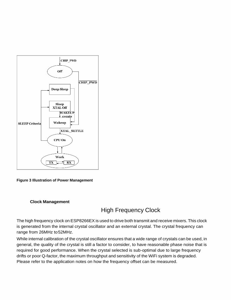
Figure 3 Illustration of Power Management
Clock Management
High Frequency Clock
The high frequency clock on ESP8266EX is used to drive both transmit and receive mixers. This clock
is generated from the internal crystal oscillator and an external crystal. The crystal frequency can
range from 26MHz to 52MHz.
While internal calibration of the crystal oscillator ensures that a wide range of crystals can be used, in
general, the quality of the crystal is still a factor to consider, to have reasonable phase noise that is
required for good performance. When the crystal selected is sub-optimal due to large frequency
drifts or poor Q-factor, the maximum throughput and sensitivity of the WiFi system is degraded.
Please refer to the application notes on how the frequency offset can be measured.
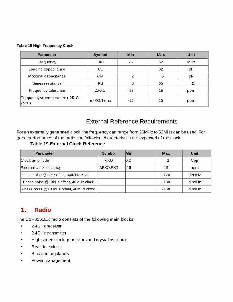
Table 18 High Frequency Clock
Parameter Symbol Min Max Unit
Frequency FXO 26 52 MHz
Loading capacitance CL 32 pF
Motional capacitance CM 2 5 pF
Series resistance RS 0 65 Ω
Frequency tolerance ΔFXO -15 15 ppm
Frequency vs temperature (-25°C ~
75°C) ΔFXO,Temp -15 15 ppm
External Reference Requirements
For an externally generated clock, the frequency can range from 26MHz to 52MHz can be used. For
good performance of the radio, the following characteristics are expected of the clock:
Table 19 External Clock Reference
Parameter Symbol Min Max Unit
Clock amplitude VXO 0.2 1 Vpp
External clock accuracy ΔFXO,EXT -15 15 ppm
Phase noise @1kHz offset, 40MHz clock -120 dBc/Hz
Phase noise @10kHz offset, 40MHz clock -130 dBc/Hz
Phase noise @100kHz offset, 40MHz clock -138 dBc/Hz
1. Radio
The ESP8266EX radio consists of the following main blocks:
• 2.4GHz receiver
• 2.4GHz transmitter
• High speed clock generators and crystal oscillator
• Real time clock
• Bias and regulators
• Power management
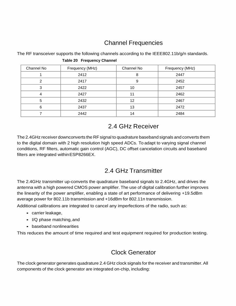
Channel Frequencies
The RF transceiver supports the following channels according to the IEEE802.11b/g/n standards.
Table 20 Frequency Channel
Channel No Frequency (MHz) Channel No Frequency (MHz)
1 2412 8 2447
2 2417 9 2452
3 2422 10 2457
4 2427 11 2462
5 2432 12 2467
6 2437 13 2472
7 2442 14 2484
2.4 GHz Receiver
The 2.4GHz receiver downconverts the RF signal to quadrature baseband signals and converts them
to the digital domain with 2 high resolution high speed ADCs. To adapt to varying signal channel
conditions, RF filters, automatic gain control (AGC), DC offset cancelation circuits and baseband
filters are integrated within ESP8266EX.
2.4 GHz Transmitter
The 2.4GHz transmitter up-converts the quadrature baseband signals to 2.4GHz, and drives the
antenna with a high powered CMOS power amplifier. The use of digital calibration further improves
the linearity of the power amplifier, enabling a state of art performance of delivering +19.5dBm
average power for 802.11b transmission and +16dBm for 802.11n transmission.
Additional calibrations are integrated to cancel any imperfections of the radio, such as:
▪ carrier leakage,
▪ I/Q phase matching, and
▪ baseband nonlinearities
This reduces the amount of time required and test equipment required for production testing.
Clock Generator
The clock generator generates quadrature 2.4 GHz clock signals for the receiver and transmitter. All
components of the clock generator are integrated on-chip, including:
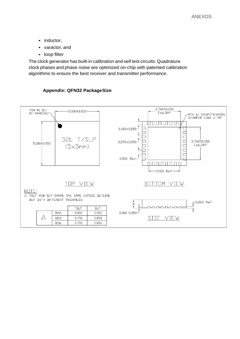
ANEXOS
▪ inductor,
▪ varactor, and
▪ loop filter
The clock generator has built-in calibration and self test circuits. Quadrature
clock phases and phase noise are optimized on-chip with patented calibration
algorithms to ensure the best receiver and transmitter performance.
Appendix: QFN32 Package Size
GLOSARIO DE SIGLAS Y ACRONIMOS
m. metros.
cm. centímetros.
mm. milímetros.
V. voltios.
dp. dioptrías.
esf. esferas.
Oled. Organic light-emitting diode.
Wifi. Wireless Fidelity.
IP. Internet Protocol.
USB. Universal Serial Bus.
I2C. Inter-Integrated Circuit.
URL. Uniform Resource Locator.
txt. text.
JAR. Java Archive.
EXE. EXEcutable
Bibliografía
Bibliografía
Arduino. Arduino Software. 2018. https://www.arduino.cc/en/main/software.
—. Language Reference. 2018. https://www.arduino.cc/reference/en/.
Clínica Baviera. Medición de la graduación: La dioptría. 11 de Enero de 2014.
https://www.clinicabaviera.com/blog/mundo-para-ver/medicion-de-la-graduacion-la-
dioptria/.
electrontools. Cómo funciona el sensor ultrasónico HC-SR04. 1 de Abril de 2016.
http://www.electrontools.com/Home/WP/2016/04/01/como-funciona-el-sensor-
ultrasonico-hc-sr04/.
González, David Carmona. Zona profesional: Entender la retinoscopía. 25 de Julio de 2011.
http://areaprofesional.blogspot.com.es/2011/07/entender-la-retinoscopia-o-
esquiascopia.html.
NetBeans. NetBeans IDE Features. 2018. https://netbeans.org/features/index.html.
Welch Allyn, Inc. Retinoscopía de franja. 30 de Marzo de 2009.
https://www.welchallyn.com/content/dam/welchallyn/documents/upload-
docs/Training-and-Use/User-Manual/usermanual_20090331_retinoscope.pdf.
WEMOS Electronics. 1-Button Shield. 2 de Mayo de 2017.
https://wiki.wemos.cc/products:d1_mini_shields:1-button_shield.
—. Battery Shield. 5 de Junio de 2017.
https://wiki.wemos.cc/products:d1_mini_shields:battery_shield.
—. D1 mini. 23 de Enero de 2018. https://wiki.wemos.cc/products:d1:d1_mini.
—. Get started in Arduino. 14 de Julio de 2017.
https://wiki.wemos.cc/tutorials:get_started:get_started_in_arduino.
—. OLED Shield. 23 de Enero de 2018.
https://wiki.wemos.cc/products:d1_mini_shields:oled_shield.