Embed Size (px)
Citation preview
Pedro Miguel Lobato Garcia
Licenciado em Ciências da Engenharia Eletrotécnica e de Computadores
Design of passive Σ∆ modulator for ESP32
Dissertação para obtenção do Grau de Mestre em
Engenharia Electrotécnica e de Computadores
Orientador: Nuno Filipe Silva Veríssimo Paulino,Professor Auxiliar,Universidade Nova de Lisboa
Júri
Presidente: Doutor Fernando José Almeida Vieira do Coito - FCT/UNLArguente: Doutor João Pedro Abreu de Oliveira - FCT/UNL
Vogal: Doutor Nuno Filipe Silva Veríssimo Paulino - FCT/UNL
Março, 2020


Copyright © Pedro Miguel Lobato Garcia, Faculty of Sciences and Technology, NOVA
University Lisbon.
The Faculty of Sciences and Technology and the NOVA University Lisbon have the right,
perpetual and without geographical boundaries, to file and publish this dissertation
through printed copies reproduced on paper or on digital form, or by any other means
known or that may be invented, and to disseminate through scientific repositories and
admit its copying and distribution for non-commercial, educational or research purposes,
as long as credit is given to the author and editor.
Este documento foi gerado utilizando o processador (pdf)LATEX, com base no template “novathesis” [1] desenvolvido no Dep. Informática da FCT-NOVA [2].[1] https://github.com/joaomlourenco/novathesis [2] http://www.di.fct.unl.pt


Aos meus pais, Gabriela e Francisco, e à minha irmã Ana.

Acknowledgements
First and foremost, I would like to acknowledge and show my appreciation to my super-
visor Prof. Nuno Paulino, for his advice, orientation, patience and availability, without
which I would have been utterly lost.
I would like to thank Prof. Rui Tavares for his technical support.
I would also like to show my appreciation and gratitude to my colleagues and friends
for all their support.
Finally, I would like to thank my family for their encouragement, motivation and
patience.
vii

Abstract
This thesis addresses the problem of voice recognition, by studying how to build a low-
cost solution for data acquisition, presents the analysis, design implementation and sim-
ulation of a low-cost continuous-time(CT) passive sigma-delta modulator(ΣΔM) with
signal-to-noise-plus-distortion ratio(SNDR) > 86dB to increase fidelity in voice recogni-
tion applications.
Employing passive RC integrators and a differential signal structure, the CT pas-
sive ΣΔM is optimized to work as independently from a specific comparator module
as possible, by decreasing the necessary gain of the comparator in the modulator gain.
Nevertheless, the loop gain is restricted by the comparator’s noise, aggravated by the high
attenuation of the passive RC integrators on the signal, causing low voltage swing at the
comparator’s input.
It is discussed the viability of utilizing a microprocessor (µP) as substitute of the
comparator block in a CT passive ΣΔM, specifically, the esp32. Due to hardware limi-
tations and the high-frequency requirements of the CT passive ΣΔM, it is proven this
substitution is not viable.
Along the course of the design implementation a comparison in the performance of
three different simulation software is presented, these software being, the open-source
LTspice VII, the open-source Ngspice and the private Cadence Virtuoso. As it was necessary
to change simulation software at different stages in the design of the circuit.
ix

Resumo
Esta tese discute o problema de reconhecimento de voz, estudando como construir uma
solução baixo custo de acquisição de dados, apresenta ainda uma análise, projecto e simu-
lação de um conversor analógico-digital(ADC), usando um modulador sigma-delta(ΣΔM)
passivo de tempo contínuo(CT) com SNDR > 86dB, para o efeito de melhorar a resolução
de aplicações de reconhecimento de voz.
Através da utilização de integradores passivos RC e uma estrutura de sinais differen-
ciais, o ΣΔM é optimizado para funcionar o mais independentemente possivel de um
comparador especifico, sendo para isso minimizado o ganho do comparador no ganho
do modulador. Contudo, o ganho do modulador é limitado pelo ruido do comparador,
agravado pelo efeito de atenuação dos integradores passivos no sinal, causando um sinal
de baixa tensão na entrada do comparador.
É discutida a viabilidade de utilizar um micro processador(µP) para substituir o mó-
dulo do comparador no ΣΔM, especificamente, o µP esp32. Devido às limitações de hard-ware e à alta frequência que é necessária para o ΣΔM, é provado que esta substituição
não é viável.
Ao decorrer do projecto do ΣΔM é apresentada a comparação de desempenho de três
software de simulação utilizados, especificamente, o LTspice VII, o Ngspice e o CadenceVirtuoso. Visto ter sido necessário a alteração de software de simulação em diferentes
fases do projecto do circuito.
xi

Contents
List of Figures xv
List of Tables xvii
Acronyms xix
1 Introduction 1
1.1 Motivation . . . . . . . . . . . . . . . . . . . . . . . . . . . . . . . . . . . . 1
1.2 Objectives . . . . . . . . . . . . . . . . . . . . . . . . . . . . . . . . . . . . 2
1.3 Document Overview . . . . . . . . . . . . . . . . . . . . . . . . . . . . . . 2
2 State Of Art 5
2.1 Voice Recognition Systems . . . . . . . . . . . . . . . . . . . . . . . . . . . 5
2.1.1 Vocca PRO Light . . . . . . . . . . . . . . . . . . . . . . . . . . . . 5
2.1.2 Honeywell Smart Thermostat . . . . . . . . . . . . . . . . . . . . . 6
2.1.3 Amazon Echo Dot . . . . . . . . . . . . . . . . . . . . . . . . . . . . 6
2.1.4 Apple HomePod . . . . . . . . . . . . . . . . . . . . . . . . . . . . . 7
2.2 Voice Recognition Software’s . . . . . . . . . . . . . . . . . . . . . . . . . . 8
2.2.1 Speech Data Acquisition . . . . . . . . . . . . . . . . . . . . . . . . 9
2.3 Microcontrollers . . . . . . . . . . . . . . . . . . . . . . . . . . . . . . . . . 10
2.3.1 ESP32 . . . . . . . . . . . . . . . . . . . . . . . . . . . . . . . . . . . 10
2.3.2 Arduino . . . . . . . . . . . . . . . . . . . . . . . . . . . . . . . . . 11
2.3.3 Raspberry Pi . . . . . . . . . . . . . . . . . . . . . . . . . . . . . . . 12
2.3.4 RDA5981A . . . . . . . . . . . . . . . . . . . . . . . . . . . . . . . . 13
2.4 Systems on a chip . . . . . . . . . . . . . . . . . . . . . . . . . . . . . . . . 14
2.4.1 ESP32 . . . . . . . . . . . . . . . . . . . . . . . . . . . . . . . . . . . 14
2.4.2 Arduino . . . . . . . . . . . . . . . . . . . . . . . . . . . . . . . . . 15
2.4.3 RDA5981A . . . . . . . . . . . . . . . . . . . . . . . . . . . . . . . . 16
2.5 ΣΔModulators . . . . . . . . . . . . . . . . . . . . . . . . . . . . . . . . . 17
2.5.1 Basic Operation of an ADC . . . . . . . . . . . . . . . . . . . . . . 17
2.5.2 Principles of ΣΔModulators . . . . . . . . . . . . . . . . . . . . . 18
2.5.3 ΣΔM Loop Filter . . . . . . . . . . . . . . . . . . . . . . . . . . . . 22
xiii
CONTENTS
3 Architecture Development 27
3.1 Circuit Design . . . . . . . . . . . . . . . . . . . . . . . . . . . . . . . . . . 27
3.1.1 Theoretical analysis . . . . . . . . . . . . . . . . . . . . . . . . . . . 27
3.1.2 ΣΔ 1st Order Modulator . . . . . . . . . . . . . . . . . . . . . . . . 27
3.2 Simulation programs . . . . . . . . . . . . . . . . . . . . . . . . . . . . . . 30
4 ΣΔ 2nd Order Modulator Development 33
4.1 ΣΔ 2nd Order Modulator Single Ended . . . . . . . . . . . . . . . . . . . 33
4.1.1 Theoretical analysis and calculations . . . . . . . . . . . . . . . . . 34
4.1.2 Electrical Simulation . . . . . . . . . . . . . . . . . . . . . . . . . . 36
4.2 ΣΔ 2nd Order Differential Modulator . . . . . . . . . . . . . . . . . . . . 38
5 ESP32 Development & Implementation 45
5.1 Viability Study for ESP32 . . . . . . . . . . . . . . . . . . . . . . . . . . . . 45
5.1.1 Theoretical Viability Study . . . . . . . . . . . . . . . . . . . . . . . 45
5.1.2 Practical Viability Study . . . . . . . . . . . . . . . . . . . . . . . . 46
6 Summary & Future Work 49
6.1 Summary . . . . . . . . . . . . . . . . . . . . . . . . . . . . . . . . . . . . . 49
6.2 Future Work . . . . . . . . . . . . . . . . . . . . . . . . . . . . . . . . . . . 50
Bibliography 51
xiv
List of Figures
2.1 VOCCA Pro . . . . . . . . . . . . . . . . . . . . . . . . . . . . . . . . . . . . . 5
2.2 Honeywell Wi-Fi Thermostat RTH9590WF1011 . . . . . . . . . . . . . . . . . 6
2.3 Amazon Echo Dot 3rd Generation . . . . . . . . . . . . . . . . . . . . . . . . . 6
2.4 Apple HomePod . . . . . . . . . . . . . . . . . . . . . . . . . . . . . . . . . . . 7
2.5 ESP32 Development board DevKitC . . . . . . . . . . . . . . . . . . . . . . . 10
2.6 Arduino Micro development board . . . . . . . . . . . . . . . . . . . . . . . . 11
2.7 Raspberry Pi 2 . . . . . . . . . . . . . . . . . . . . . . . . . . . . . . . . . . . . 12
2.8 RDA5981a development board . . . . . . . . . . . . . . . . . . . . . . . . . . 13
2.9 System structure block diagram . . . . . . . . . . . . . . . . . . . . . . . . . . 14
2.10 System address mapping . . . . . . . . . . . . . . . . . . . . . . . . . . . . . . 15
2.11 (a) Conceptual block diagram of a generic LP ADC (b) Signal Processing . . 17
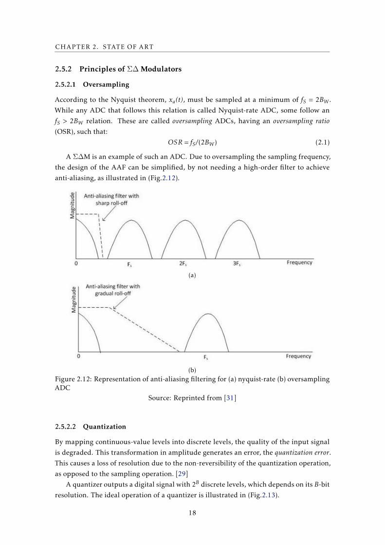
2.12 Representation of anti-aliasing filtering for (a) nyquist-rate (b) oversampling
ADC . . . . . . . . . . . . . . . . . . . . . . . . . . . . . . . . . . . . . . . . . . 18
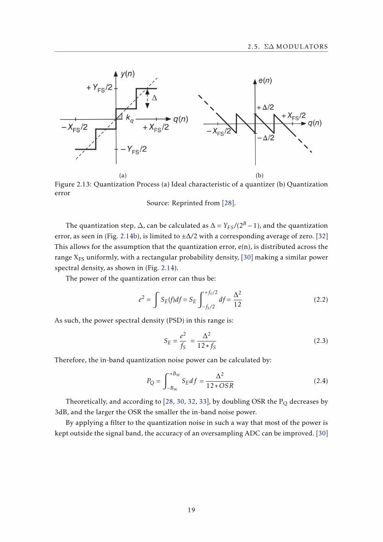
2.13 Quantization Process (a) Ideal characteristic of a quantizer (b) Quantization
error . . . . . . . . . . . . . . . . . . . . . . . . . . . . . . . . . . . . . . . . . . 19
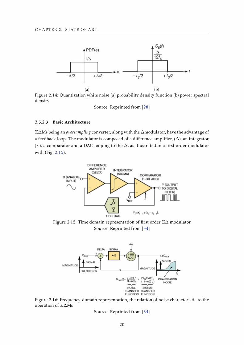
2.14 Quantization white noise (a) probability density function (b) power spectral
density . . . . . . . . . . . . . . . . . . . . . . . . . . . . . . . . . . . . . . . . 20
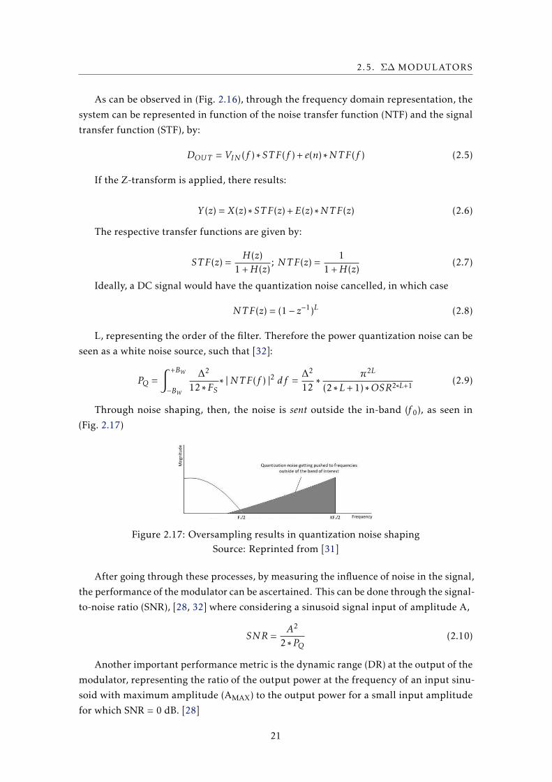
2.15 Time domain representation of first order ΣΔmodulator . . . . . . . . . . . 20
2.16 Frequency-domain representation, the relation of noise characteristic to the
operation of ΣΔMs . . . . . . . . . . . . . . . . . . . . . . . . . . . . . . . . . 20
2.17 Oversampling results in quantization noise shaping . . . . . . . . . . . . . . 21
2.18 RC passive integrator . . . . . . . . . . . . . . . . . . . . . . . . . . . . . . . . 24
2.19 2nd order ΣΔM with feedforward structure (a) block diagram (b) circuit rep-
resentation . . . . . . . . . . . . . . . . . . . . . . . . . . . . . . . . . . . . . . 24
3.1 Solution Block Diagram . . . . . . . . . . . . . . . . . . . . . . . . . . . . . . 27
3.2 1st order ΣΔ modulator Block Diagram . . . . . . . . . . . . . . . . . . . . . 28
3.3 1st order ΣΔ modulator Simulation Schematic . . . . . . . . . . . . . . . . . 28
3.4 1st order ΣΔmodulator FFT in LTspice VII . . . . . . . . . . . . . . . . . . . . 29
3.5 2nd OrderΣΔ SE Modulator FFT with 0dBV Input Signal Amplitude (a) LTspiceVII (b) Ngspice . . . . . . . . . . . . . . . . . . . . . . . . . . . . . . . . . . . . 30
xv
LIST OF FIGURES
3.6 2nd Order ΣΔ SE Modulator FFT with -13dBV Input Signal Amplitude (a)
LTspice VII (b) Ngspice . . . . . . . . . . . . . . . . . . . . . . . . . . . . . . . 30
4.1 2nd Order ΣΔModulator Block Diagram . . . . . . . . . . . . . . . . . . . . . 33
4.2 2nd Integrator with Zero Block Diagram . . . . . . . . . . . . . . . . . . . . . 34
4.3 2nd Order ΣΔModulator Circuit Schematic . . . . . . . . . . . . . . . . . . . 34
4.4 STF & NTF . . . . . . . . . . . . . . . . . . . . . . . . . . . . . . . . . . . . . . 36
4.5 2nd Order ΣΔ Single-ended Modulator SINAD . . . . . . . . . . . . . . . . . 36
4.6 2nd Order ΣΔ Single-ended Modulator FFT in Ngspice . . . . . . . . . . . . . 37
4.7 2nd Order ΣΔ Single-ended Modulator Noiseless FFT in Virtuoso . . . . . . 37
4.8 2nd Order ΣΔ SE Modulator Noise FFT in Virtuoso (a) Noise < 16MHz (b)
Noise < 32MHz (c) Noise < 80MHz . . . . . . . . . . . . . . . . . . . . . . . . 38
4.9 2nd Order ΣΔ Differential Modulator Electrical Schematic . . . . . . . . . . . 38
4.10 2nd Order ΣΔ Differential Modulator SINAD in Virtuoso . . . . . . . . . . . 39
4.11 2nd Order ΣΔ Differential Modulator Noiseless FFT in Virtuoso . . . . . . . 39
4.12 2nd OrderΣΔDifferential Modulator Noise FFT in Virtuoso (a) Noise < 16MHz
(b) Noise < 32MHz (c) Noise < 80MHz . . . . . . . . . . . . . . . . . . . . . . 40
4.13 2nd Order ΣΔ Differential Modulator Capacitors 10% Variation FFT in Virtu-oso (a) C1 (b) C2 . . . . . . . . . . . . . . . . . . . . . . . . . . . . . . . . . . . 40
4.14 2nd Order ΣΔ Differential Modulator Resistors 10% Variation FFT in Virtuoso(a) R1 (b) R2 (c) R3 (d) R4 . . . . . . . . . . . . . . . . . . . . . . . . . . . . . 41
4.15 2nd Order ΣΔ Differential Modulator Capacitors 20% Variation FFT in Virtu-oso (a) C1 (b) C2 . . . . . . . . . . . . . . . . . . . . . . . . . . . . . . . . . . . 41
4.16 2nd Order ΣΔ Differential Modulator Resistors 20% Variation FFT in Virtuoso(a) R1 (b) R2 (c) R3 (d) R4 . . . . . . . . . . . . . . . . . . . . . . . . . . . . . 42
4.17 2nd Order ΣΔ Differential Modulator Comparator Offset Variation FFT in Vir-tuoso (a) 10% (200mV) (b) 7% (100mV) . . . . . . . . . . . . . . . . . . . . . . 42
5.1 ESP32 GPIO Loop at 8KHz (a) Input (b) Output . . . . . . . . . . . . . . . . . 46
5.2 ESP32 GPIO Loop at 80KHz (a) Input (b) Output . . . . . . . . . . . . . . . . 47
5.3 ESP32 GPIO Loop at 8MHz (a) Input (b) Output . . . . . . . . . . . . . . . . 47
xvi
List of Tables
2.1 System examples comparison . . . . . . . . . . . . . . . . . . . . . . . . . . . 7
2.2 Audio data rate vs. sound quality . . . . . . . . . . . . . . . . . . . . . . . . . 9
2.3 Passive ΣΔMs: CT VS DT . . . . . . . . . . . . . . . . . . . . . . . . . . . . . . 25
3.1 Resistors values . . . . . . . . . . . . . . . . . . . . . . . . . . . . . . . . . . . 29
3.2 Simulation Comparison: LTspice VII VS Ngspice . . . . . . . . . . . . . . . . . 31
4.1 Circuit and Frequency values . . . . . . . . . . . . . . . . . . . . . . . . . . . 35
4.2 Theoretical Results . . . . . . . . . . . . . . . . . . . . . . . . . . . . . . . . . 38
4.3 Result of Component Variation . . . . . . . . . . . . . . . . . . . . . . . . . . 43
6.1 Simulation Programs Comparison . . . . . . . . . . . . . . . . . . . . . . . . . 49
xvii

Acronyms
Σ∆M Sigma-Delta Modulator.
∆ Delta.
Σ Sigma.
µP Micro Processor.
BW Bandwidth.
fP Pole Frequency.
fS Sampling Frequency.
AAF Anti-aliasing Filter.
ADC Analog to Digital Converter.
ARM Advanced RISC Machine.
BLE Bluetooth Low Energy.
C Capacitor.
CPU Central Processing Unit.
CT Continuous Time.
DAC Digital to Analog Converter.
DIY Do It Yourself.
DR Dynamic Range.
DT Discrete Time.
EEPROM Electrically Erasable Programmable Read-only Memory.
FAT File Allocation Table.
FFT Fast Fourier Transform.
GPIO General-purpose Input/Output.
xix
ACRONYMS
I/O Input/Output.
I2C Multi-Master Bus.
I2S Integrated Inter-IC Sound Bus.
IC Integrated Circuit.
ICSP In-Circuit Serial Programming.
IDE Integrated Development Environment.
IoT Internet of Things.
IP Internet Protocol.
MCU Microcontroller.
MQTT MQ Telemetry Transport.
NLP Natural Language Processing.
NTF Noise Transfer Function.
OSR Oversampling Ratio.
OTA Operational Transconductance Amplifier.
PSD Power Spectral Density.
PSRAM Pseudo-static Random-access Memory.
PWM Pulse Width Modulation.
R Resistor.
RAM Random-access Memory.
rms root-square-mean.
RTOS Real-time Operating System.
S/H Sample and Hold.
SC Switched-capacitor.
SDIO Secure Digital Input/Output.
SINAD Signal-to-Noise and Distortion ratio.
SNDR Signal-to-Noise-plus-Distortion Ratio.
SNR Signal-to-Noise Ratio.
SoC System on a Chip.
SPi Serial Peripheral Interface.
SRAM Static Random-access Memory.
xx

ACRONYMS
SSL Secure Sockets Layer.
STF Signal Transfer Function.
TCP Transmission Control Protocol.
TEQ Time Encoded Quantization.
UART Universal Asynchronous Receiver/Transmitter.
ULP Ultra-Low Power.
USB Universal Serial Bus.
xxi

Chapter
1Introduction
1.1 Motivation
Technology is ever more present in everyday life. Nowadays, more than ever before, we
are dependant on the ease and comfort proportioned by the technological advances that
have boomed in the past few years. This dependence tends to become heavier with even
more advances and tends to accelerate the development of technology. More so on the
side of IoT (Internet of Things) as it is the development of this type of technology which
allows us more comfort and connectivity to the world and others.
Also due to the spread and ease of access of DIY development kits and cheap tech-
nology, the IoT and home automation industries have seen rapid advances, and have
garnered significant interest from the industry to the tech-savvy hobbyists.
In IoT and home automation, there are various areas to take into account when devel-
oping a device, or various devices depending on the needs of the user. However, one area
that is always needed and of utmost importance is sensors and analysis of the data they
gather.
IoT works through sensors, they are the bridge between the physical world and the
digital world [1]. Home automation as an application of IoT works in much the same way.
With a special focus on the interaction of the user with the home, through interfaces such
as "Alexa" and other such systems which we will delve into deeper detail further on in
this document.
These interactions usually happen through various ways which have been developed
to cope with specific necessities and convenience of the user. As is the example of voice
recognition systems or software application, in either a mobile phone or computer, even
gesture recognition has been attempted to interface with home automation systems [2–4].
1
CHAPTER 1. INTRODUCTION
So that these systems can work on a single device, we need devices powerful and
capable enough to receive and process the information created by the user. It is the
case that microcontrollers (MCUs) are just one of the cheapest and supported tools for
that end. There is however, the caveat that the cheaper and more powerful options
among these devices as is the case of the ESP32 do not have the best on analog to digital
converter (ADC) technologies, which are of high importance when you want to have
reliable, accurate voice control over a device.
When talking about home automation, due to its many concerns about privacy and
security, many, choose to go about it on theirs own terms. Turning to small developers, or
trying at their own hand to implement a system in their homes. For these people, securing
cheap but quality products is paramount, even at the cost of a full natural language
recognition system. For many cases, this might be unnecessary, as simple commands can
do the job, while not having to put their private information at risk.
1.2 Objectives
This work, aims to develop a cost-effective high resolution external ADC shield for the
ESP32 to further improve its voice recognition capabilities and therefore augmenting its
versatility and usability. With a special focus on uses such as home automation that can
work both over the internet or locally without a connection.
This work’s goal is to design a sigma-delta passive modulator, due to its specific
characteristics in integrated circuits, to work as a high resolution ADC in conjunction with
the ESP32, in which the ESP32 will substitute the the sigma-delta passive modulator’s
comparator module.
In order to have a proper solution, a succinct market search will be necessary. An
appraisal of what is already available, that might compete with our solution to solve
domestic implementation of home automation with voice control.
1.3 Document Overview
This document is structured in the following way:
• Chapter 2 presents a small market search representative of today’s mainstream
voice recognition devices. Is also presented the State-of-Art technology in voice
recognition software, as well as an introduction to the concept of speech acquisition
and the function of sigma-delta modulators. The microprocessors with biggest
community support are discussed and compared.
• Chapter 3 describes some accomplished preparatory research into the first steps of
development of the proposed project.
• Chapter 4 presents a time table for the work to be developed.
2

1.3. DOCUMENT OVERVIEW
• Chapter 5 Studies the viability of using an ESP32 microprocessor(µP), both per its
theoretical capabilities as well as with practical tests.
• Chapter 6 Summarises this work along with what can be interesting to make a
follow-up study, in a future work section.
3


Chapter
2State Of Art
2.1 Voice Recognition Systems
As we have seen before, voice recognition is being more and more developed and sought
after, due to the possibilities of convenience and ease of use it can provide when fully
matured.
As can be seen in these next few examples the more widespread usage of voice recogni-
tion in home automation restricts the user to specific devices or specific platforms such as
the HomePod being attached to Siri and Apple compatible smart devices. Though there
might be a few devices trying to make their stand, usually, the cost to make an appealing
device pushes its price up more than users are willing to spend, besides the compatibility
issues that might arise.
From here, we will see some examples of developed systems already available for
customers, from simple gadgets to smart home hubs:
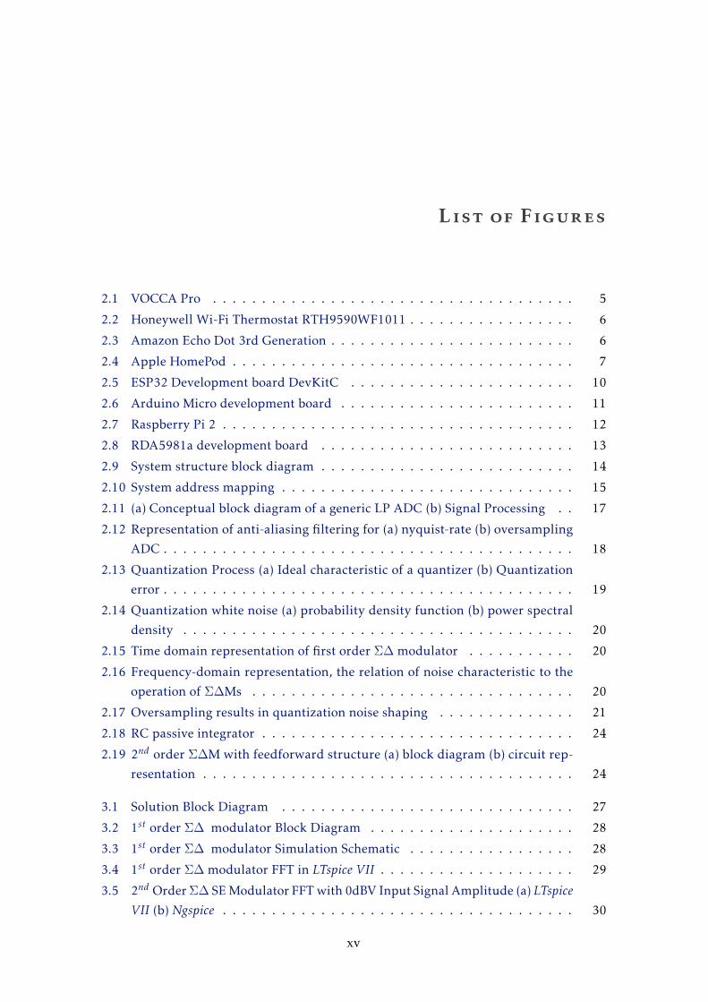
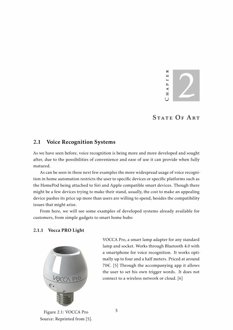
2.1.1 Vocca PRO Light
Figure 2.1: VOCCA Pro
Source: Reprinted from [5].
VOCCA Pro, a smart lamp adapter for any standard
lamp and socket. Works through Bluetooth 4.0 with
a smartphone for voice recognition. It works opti-
mally up to four and a half meters. Priced at around
70€. [5] Through the accompanying app it allows
the user to set his own trigger words. It does not
connect to a wireless network or cloud. [6]
5
CHAPTER 2. STATE OF ART
2.1.2 Honeywell Smart Thermostat
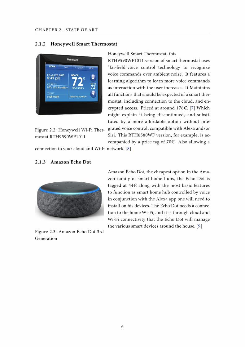
Figure 2.2: Honeywell Wi-Fi Ther-
mostat RTH9590WF1011
Honeywell Smart Thermostat, this
RTH9590WF1011 version of smart thermostat uses
"far-field"voice control technology to recognize
voice commands over ambient noise. It features a
learning algorithm to learn more voice commands
as interaction with the user increases. It Maintains
all functions that should be expected of a smart ther-
mostat, including connection to the cloud, and en-
crypted access. Priced at around 176€. [7] Which
might explain it being discontinued, and substi-
tuted by a more affordable option without inte-
grated voice control, compatible with Alexa and/or
Siri. This RTH6580WF version, for example, is ac-
companied by a price tag of 70€. Also allowing a
connection to your cloud and Wi-Fi network. [8]
2.1.3 Amazon Echo Dot
Figure 2.3: Amazon Echo Dot 3rd
Generation
Amazon Echo Dot, the cheapest option in the Ama-
zon family of smart home hubs, the Echo Dot is
tagged at 44€ along with the most basic features
to function as smart home hub controlled by voice
in conjunction with the Alexa app one will need to
install on his devices. The Echo Dot needs a connec-
tion to the home Wi-Fi, and it is through cloud and
Wi-Fi connectivity that the Echo Dot will manage
the various smart devices around the house. [9]
6
2.1. VOICE RECOGNITION SYSTEMS
2.1.4 Apple HomePod
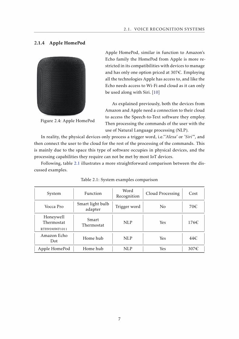
Figure 2.4: Apple HomePod
Apple HomePod, similar in function to Amazon’s
Echo family the HomePod from Apple is more re-
stricted in its compatibilities with devices to manage
and has only one option priced at 307€. Employing
all the technologies Apple has access to, and like the
Echo needs access to Wi-Fi and cloud as it can only
be used along with Siri. [10]
As explained previously, both the devices from
Amazon and Apple need a connection to their cloud
to access the Speech-to-Text software they employ.
Then processing the commands of the user with the
use of Natural Language processing (NLP).
In reality, the physical devices only process a trigger word, i.e."’Alexa’ or ’Siri’", and
then connect the user to the cloud for the rest of the processing of the commands. This
is mainly due to the space this type of software occupies in physical devices, and the
processing capabilities they require can not be met by most IoT devices.
Following, table 2.1 illustrates a more straightforward comparison between the dis-
cussed examples.
Table 2.1: System examples comparison
System FunctionWord
RecognitionCloud Processing Cost
Vocca ProSmart light bulb
adapterTrigger word No 70€
HoneywellThermostat
RTH9590WF1011
SmartThermostat
NLP Yes 176€
Amazon EchoDot
Home hub NLP Yes 44€
Apple HomePod Home hub NLP Yes 307€
7
CHAPTER 2. STATE OF ART
2.2 Voice Recognition Software’s
Voice recognition technology has already come a long way in its development. Being one
of the big focus of the developers of this technology to assure high accuracy, for that is
what makes or breaks a good voice recognition software.
As the technology becomes more and more accurate, it will start to have a more
widespread impact on our interactions with the digital world, as humans have an easier
time speaking more words than they can write in the same time.
Some big companies though, already have very satisfying levels. An example of such
companies, we have Baidu, China’s search engine has achieved 96% accuracy in low noise
environments; Hound from SoundHound company, Siri from Apple and Google Now
from Google, are others such that have achieved similar rates of accuracy above 90%.
And while some of these might not achieve a rate as high as shown by Baidu’s, they
compensate by integrating learning algorithms that learn the user’s speech specificities
such as dialect and way of speaking, the more the user interacts with the program. As is
the case of Alexa from Amazon. [11]
These technologies though, are all under restricted access to their parent companies
and not accessible to developers and the public. There are, however, already some open
source tools to allow developers and hobbyists to use speech recognition in their various
applications.
Some platforms, like Mycroft, offer free and reliable tools for wake word detection and
speech to text for use in any project a developer might need, it requires, however, further
development to be ready for mainstream availability, being more suited for developers
and hobbyists. [12]
These tools include mainly a package developed by Carnegie Mellon University, the
CMUSphinx, and more specifically the PocketSphinx is a lighter more portable version of
their speech recognition engine which bases its technology on a database of sounds-[12],
there is also the more recently adopted, Precise, which is based on a neural network to
train wake words. [12]
There is also the community-oriented Home Assistant being developed, and while
not being a voice recognition software, this technology is encompassed in their work, and
because there is a big community feeling, everything is open source and mostly modular.
One thing they do try to do differently though is to make sure the home automation
system does not need to rely on the cloud to work. As the founder Paulus Schoutsen said,
"The cloud should be treated as an extension to your smart home instead of running it." [13]
While there are numerous more advanced open-source and restricted speech recogni-
tion software, most would not be able to be utilised locally due to their size and computing
resource constraints.
8
2.2. VOICE RECOGNITION SOFTWARE’S
2.2.1 Speech Data Acquisition
To capture voice signals, there needs to be a microphone so it can emulate the auditory
system, converting pressure waves into a time-varying electrical signal. For this purpose,
one can use condenser, electret, dynamic or carbon button microphones, each with their
advantages and disadvantages. Typically, for high-quality recordings, condenser micro-
phones are preferred, however, even the cheap electret microphones can deliver a good
recording.
Besides the circuit on which a microphone is based, there also needs to be some con-
sideration on the directional pattern one uses, depending on the use the microphone will
be given. An omnidirectional microphone will be preferred when trying to pick up sound
from all directions, however, it will also pick up more noise than a cardioid microphone
which is more precise when the location of the speaker can be guaranteed. [14]
To process the analog signal produced by the microphone, the necessity of sampling
and digitization through an analog-to-digital converter (ADC), will be made apparent.
These operations will be explained in more detail further in the document.
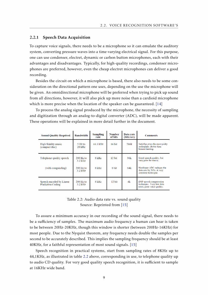
Table 2.2: Audio data rate vs. sound qualitySource: Reprinted from [15]
To assure a minimum accuracy in our recording of the sound signal, there needs to
be a sufficiency of samples. The maximum audio frequency a human can hear is taken
to be between 20Hz-20KHz, though this window is shorter (between 200Hz-16KHz) for
most people. Due to the Nyquist theorem, any frequency needs double the samples per
second to be accurately described. This implies the sampling frequency should be at least
40KHz, for a faithful representation of most sound signals. [15]
Speech recognition in practical systems, start from sampling rates of 8KHz up to
44,1KHz, as illustrated in table 2.2 above, corresponding in use, to telephone quality up
to audio CD quality. For very good quality speech recognition, it is sufficient to sample
at 16KHz wide band.
9
CHAPTER 2. STATE OF ART
After a signal has been sampled it needs to be quantized and turned into digital
information, these samples for the aforementioned values, are typically restricted to a
finite set of digital values, N = 8 to 16, being more common, and representing high-fidelity
at 16bit quantization. [14]
2.3 Microcontrollers
This section will discuss, generally, what are some of the more popular and interesting
microprocessors (µP) to use in the development of a small cost-effective device with voice
recognition capabilities, which creates a certain limiting factor in processing power and
cost, of said µPs.
2.3.1 ESP32
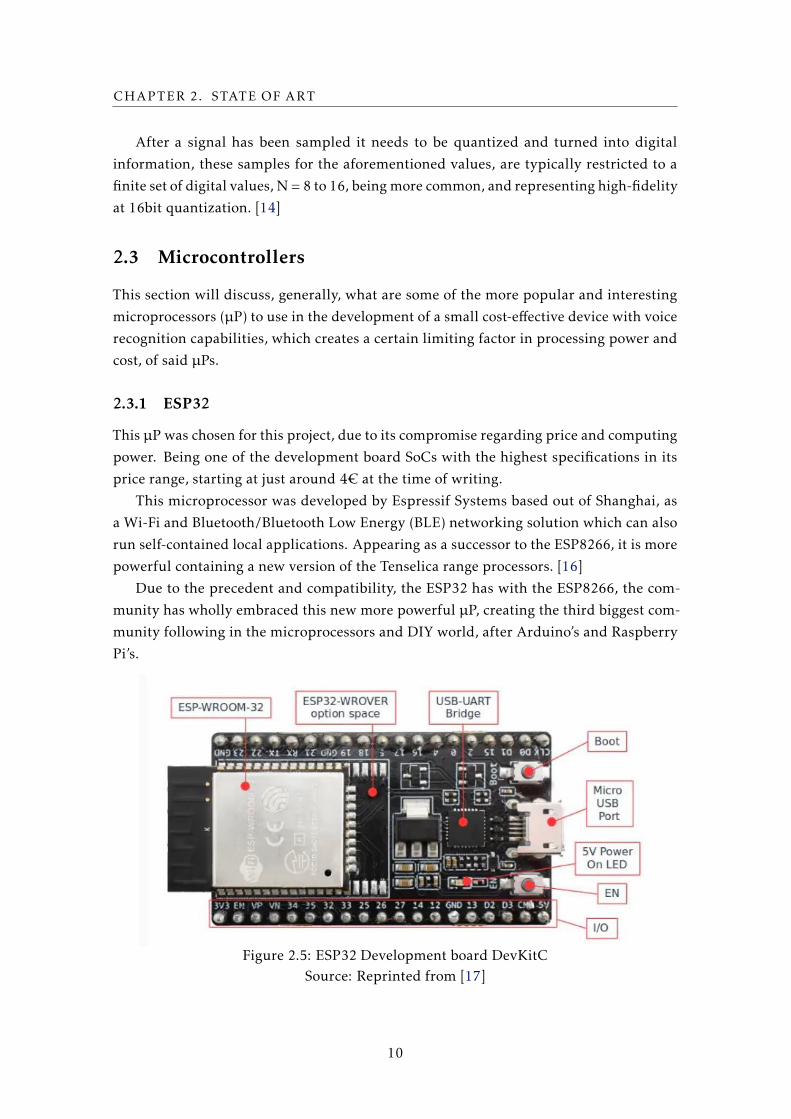
This µP was chosen for this project, due to its compromise regarding price and computing
power. Being one of the development board SoCs with the highest specifications in its
price range, starting at just around 4€ at the time of writing.
This microprocessor was developed by Espressif Systems based out of Shanghai, as
a Wi-Fi and Bluetooth/Bluetooth Low Energy (BLE) networking solution which can also
run self-contained local applications. Appearing as a successor to the ESP8266, it is more
powerful containing a new version of the Tenselica range processors. [16]
Due to the precedent and compatibility, the ESP32 has with the ESP8266, the com-
munity has wholly embraced this new more powerful µP, creating the third biggest com-
munity following in the microprocessors and DIY world, after Arduino’s and Raspberry
Pi’s.
Figure 2.5: ESP32 Development board DevKitCSource: Reprinted from [17]
10
2.3. MICROCONTROLLERS
2.3.2 Arduino
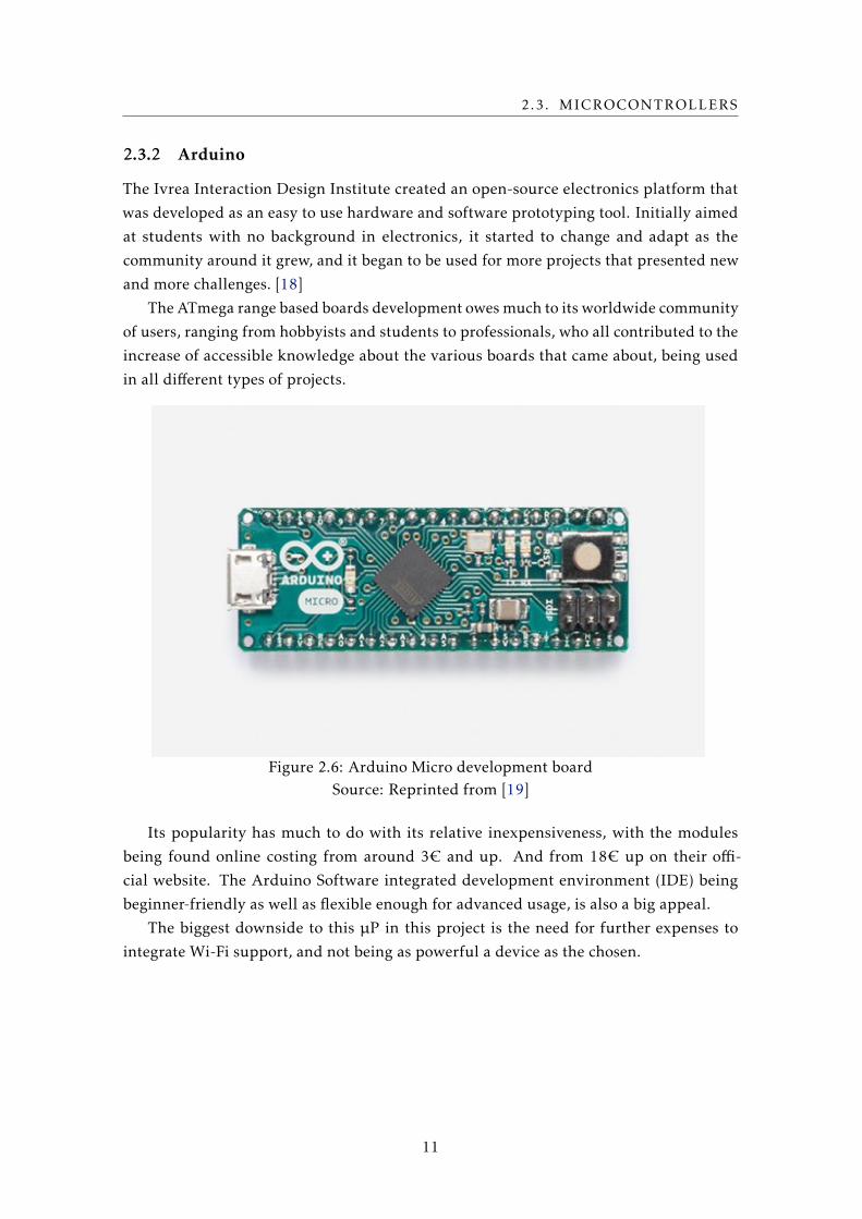
The Ivrea Interaction Design Institute created an open-source electronics platform that
was developed as an easy to use hardware and software prototyping tool. Initially aimed
at students with no background in electronics, it started to change and adapt as the
community around it grew, and it began to be used for more projects that presented new
and more challenges. [18]
The ATmega range based boards development owes much to its worldwide community
of users, ranging from hobbyists and students to professionals, who all contributed to the
increase of accessible knowledge about the various boards that came about, being used
in all different types of projects.
Figure 2.6: Arduino Micro development boardSource: Reprinted from [19]
Its popularity has much to do with its relative inexpensiveness, with the modules
being found online costing from around 3€ and up. And from 18€ up on their offi-
cial website. The Arduino Software integrated development environment (IDE) being
beginner-friendly as well as flexible enough for advanced usage, is also a big appeal.
The biggest downside to this µP in this project is the need for further expenses to
integrate Wi-Fi support, and not being as powerful a device as the chosen.
11
CHAPTER 2. STATE OF ART
2.3.3 Raspberry Pi
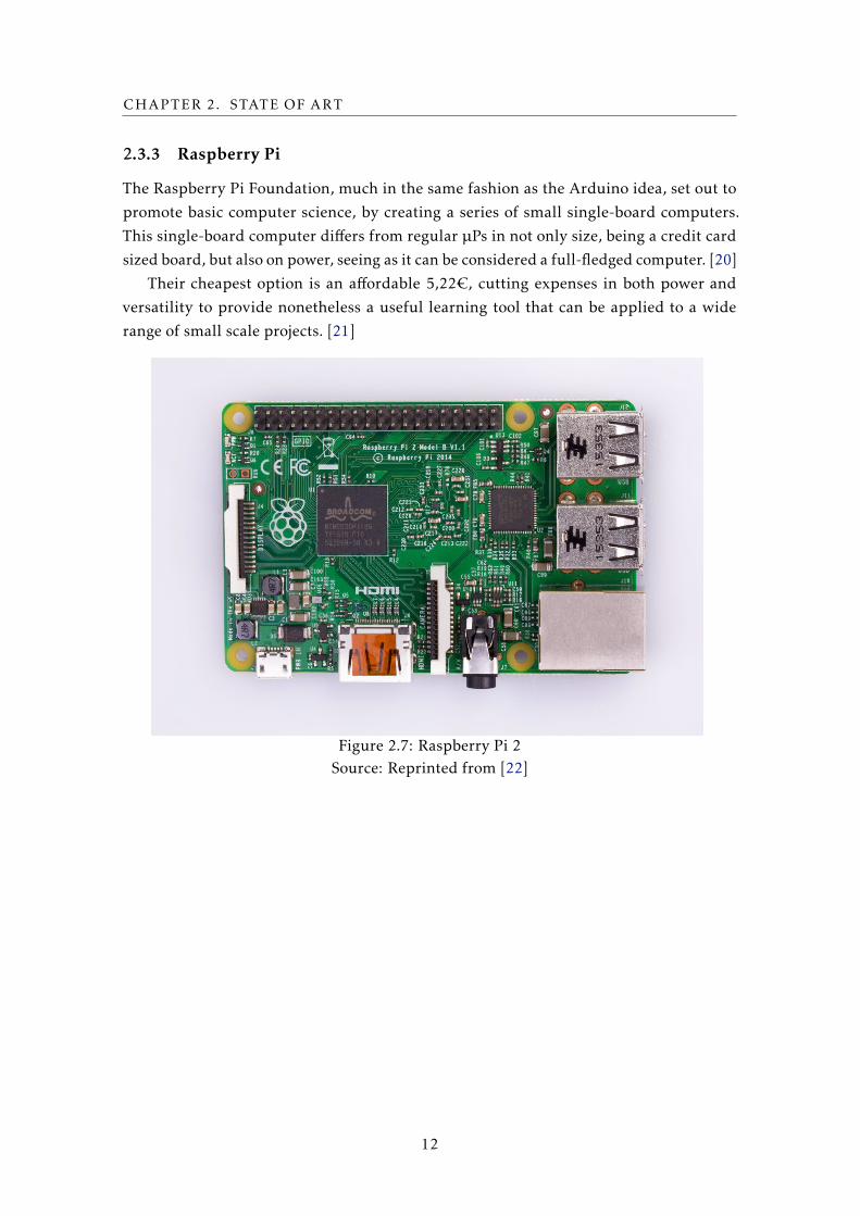
The Raspberry Pi Foundation, much in the same fashion as the Arduino idea, set out to
promote basic computer science, by creating a series of small single-board computers.
This single-board computer differs from regular µPs in not only size, being a credit card
sized board, but also on power, seeing as it can be considered a full-fledged computer. [20]
Their cheapest option is an affordable 5,22€, cutting expenses in both power and
versatility to provide nonetheless a useful learning tool that can be applied to a wide
range of small scale projects. [21]
Figure 2.7: Raspberry Pi 2Source: Reprinted from [22]
12
2.3. MICROCONTROLLERS
2.3.4 RDA5981A
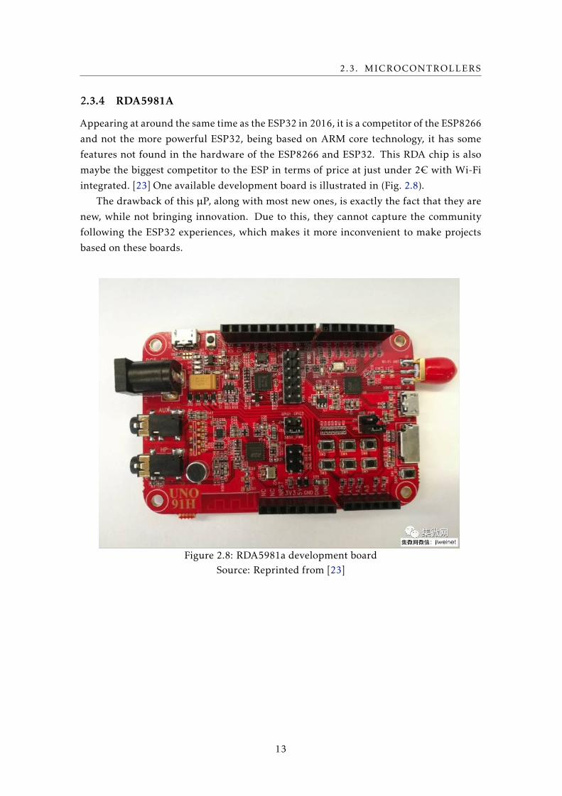
Appearing at around the same time as the ESP32 in 2016, it is a competitor of the ESP8266
and not the more powerful ESP32, being based on ARM core technology, it has some
features not found in the hardware of the ESP8266 and ESP32. This RDA chip is also
maybe the biggest competitor to the ESP in terms of price at just under 2€ with Wi-Fi
integrated. [23] One available development board is illustrated in (Fig. 2.8).
The drawback of this µP, along with most new ones, is exactly the fact that they are
new, while not bringing innovation. Due to this, they cannot capture the community
following the ESP32 experiences, which makes it more inconvenient to make projects
based on these boards.
Figure 2.8: RDA5981a development boardSource: Reprinted from [23]
13
CHAPTER 2. STATE OF ART
2.4 Systems on a chip
In this section, we will discuss the various features and specifications of the devices in
study. Due to the wide range of devices on each brand, we will study the most affordable
devices on each.
The Raspberry Pi will not be included, as it is not a microprocessor and its price
towers above the others under consideration.
2.4.1 ESP32
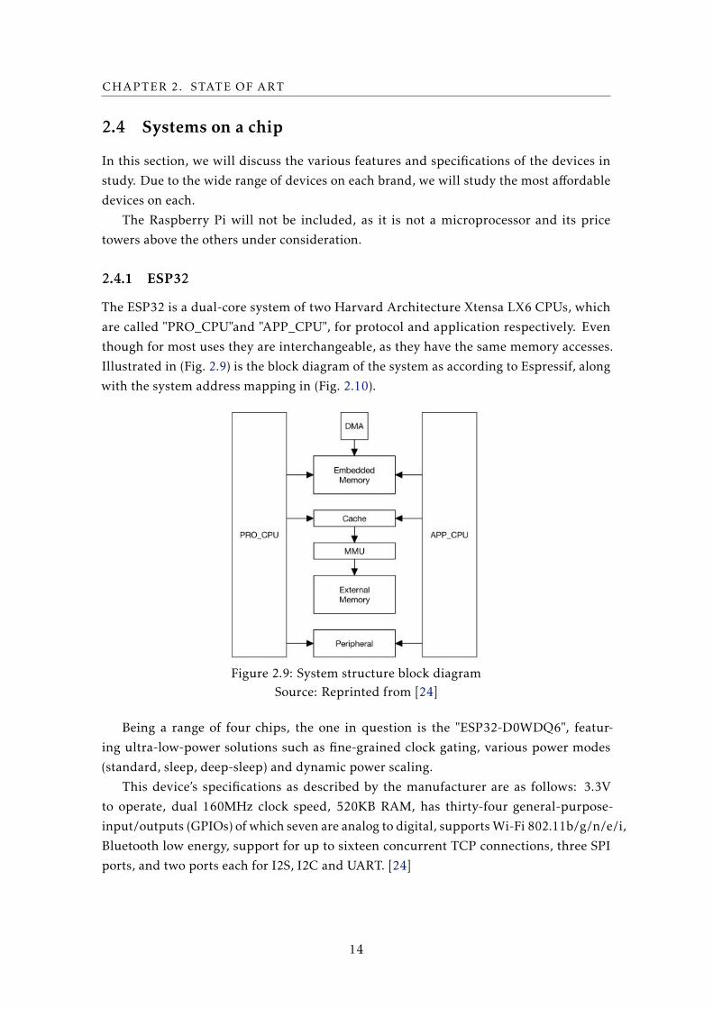
The ESP32 is a dual-core system of two Harvard Architecture Xtensa LX6 CPUs, which
are called "PRO_CPU"and "APP_CPU", for protocol and application respectively. Even
though for most uses they are interchangeable, as they have the same memory accesses.
Illustrated in (Fig. 2.9) is the block diagram of the system as according to Espressif, along
with the system address mapping in (Fig. 2.10).
Figure 2.9: System structure block diagramSource: Reprinted from [24]
Being a range of four chips, the one in question is the "ESP32-D0WDQ6", featur-
ing ultra-low-power solutions such as fine-grained clock gating, various power modes
(standard, sleep, deep-sleep) and dynamic power scaling.
This device’s specifications as described by the manufacturer are as follows: 3.3V
to operate, dual 160MHz clock speed, 520KB RAM, has thirty-four general-purpose-
input/outputs (GPIOs) of which seven are analog to digital, supports Wi-Fi 802.11b/g/n/e/i,
Bluetooth low energy, support for up to sixteen concurrent TCP connections, three SPI
ports, and two ports each for I2S, I2C and UART. [24]
14
2.4. SYSTEMS ON A CHIP
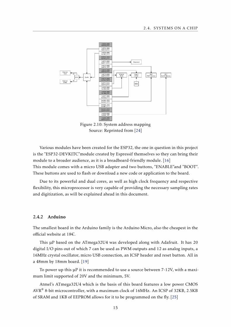
Figure 2.10: System address mappingSource: Reprinted from [24]
Various modules have been created for the ESP32, the one in question in this project
is the "ESP32-DEVKITC"module created by Espressif themselves so they can bring their
module to a broader audience, as it is a breadboard-friendly module. [16]
This module comes with a micro USB adapter and two buttons, "ENABLE"and "BOOT".
These buttons are used to flash or download a new code or application to the board.
Due to its powerful and dual cores, as well as high clock frequency and respective
flexibility, this microprocessor is very capable of providing the necessary sampling rates
and digitization, as will be explained ahead in this document.
2.4.2 Arduino
The smallest board in the Arduino family is the Arduino Micro, also the cheapest in the
official website at 18€.
This µP based on the ATmega32U4 was developed along with Adafruit. It has 20
digital I/O pins out of which 7 can be used as PWM outputs and 12 as analog inputs, a
16MHz crystal oscillator, micro USB connection, an ICSP header and reset button. All in
a 48mm by 18mm board. [19]
To power up this µP it is recommended to use a source between 7-12V, with a maxi-
mum limit supported of 20V and the minimum, 5V.
Atmel’s ATmega32U4 which is the basis of this board features a low power CMOS
AVR® 8-bit microcontroller, with a maximum clock of 16MHz. An ICSP of 32KB, 2.5KB
of SRAM and 1KB of EEPROM allows for it to be programmed on the fly. [25]
15
CHAPTER 2. STATE OF ART
2.4.3 RDA5981A
Developed with IoT, smart home, Wi-Fi speaker/home audio and smartwatch applications
as its main focus, this low-power µP provides TCP/IP protocols along with SSL with its
fully integrated 2.4GHz 802.11b/g/n MAC/PHY/radio. Contained in a compact 5x5mm2
QFN package, 0,4mm pitch QFN-40.
The Board is based on an ARM Contex M4 + FPU/MPU core, with a clock frequency
of 160MHz. The µP leaves up to 288KB SRAM for the user and uses 160KB SRAM for the
Wi-Fi stack and flash cache making a total of 448KB SRAM. Despite that, it also includes
32Mb SPI flash memory and allows for a PSRAM expansion of up to 64M. [23]
On another note, it comes integrated with a USB 2.0 interface, supporting only the
FAT file system, and has an SDIO that allows a 256G SD card. To power it up, one would
need between 3.0-3.5V.
In the matter of pins, we have two serial pins, two I2S, one I2C, four SPI, eight PWM,
two 10-bit ADCs, fourteen GPIOs available for interrupts.
In terms of software, this µP supports MQTT, smartconfig, airkiss, between others, all on
a mbed RTOS operating system. [26]
16
2.5. ΣΔ MODULATORS
2.5 ΣΔModulators
This section will present a simple and general introduction to the functioning and basic
architectures of ΣΔmodulators (ΣΔM), as well as go in more depth on the realization of
passive continuous-time ΣΔMs purposed for speech recognition.
2.5.1 Basic Operation of an ADC
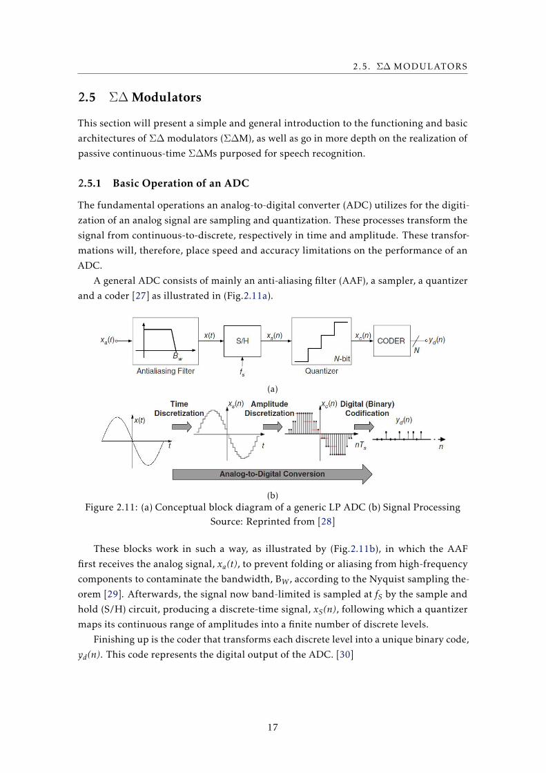
The fundamental operations an analog-to-digital converter (ADC) utilizes for the digiti-
zation of an analog signal are sampling and quantization. These processes transform the
signal from continuous-to-discrete, respectively in time and amplitude. These transfor-
mations will, therefore, place speed and accuracy limitations on the performance of an
ADC.
A general ADC consists of mainly an anti-aliasing filter (AAF), a sampler, a quantizer
and a coder [27] as illustrated in (Fig.2.11a).
(a)
(b)Figure 2.11: (a) Conceptual block diagram of a generic LP ADC (b) Signal Processing
Source: Reprinted from [28]
These blocks work in such a way, as illustrated by (Fig.2.11b), in which the AAF
first receives the analog signal, xa(t), to prevent folding or aliasing from high-frequency
components to contaminate the bandwidth, BW, according to the Nyquist sampling the-
orem [29]. Afterwards, the signal now band-limited is sampled at fS by the sample and
hold (S/H) circuit, producing a discrete-time signal, xS(n), following which a quantizer
maps its continuous range of amplitudes into a finite number of discrete levels.
Finishing up is the coder that transforms each discrete level into a unique binary code,
yd(n). This code represents the digital output of the ADC. [30]
17
CHAPTER 2. STATE OF ART
2.5.2 Principles of ΣΔModulators
2.5.2.1 Oversampling
According to the Nyquist theorem, xa(t), must be sampled at a minimum of fS = 2BW.
While any ADC that follows this relation is called Nyquist-rate ADC, some follow an
fS > 2BW relation. These are called oversampling ADCs, having an oversampling ratio(OSR), such that:
OSR = fS/(2BW) (2.1)
A ΣΔM is an example of such an ADC. Due to oversampling the sampling frequency,
the design of the AAF can be simplified, by not needing a high-order filter to achieve
anti-aliasing, as illustrated in (Fig.2.12).
(a)
(b)Figure 2.12: Representation of anti-aliasing filtering for (a) nyquist-rate (b) oversamplingADC
Source: Reprinted from [31]
2.5.2.2 Quantization
By mapping continuous-value levels into discrete levels, the quality of the input signal
is degraded. This transformation in amplitude generates an error, the quantization error.
This causes a loss of resolution due to the non-reversibility of the quantization operation,
as opposed to the sampling operation. [29]
A quantizer outputs a digital signal with 2B discrete levels, which depends on its B-bit
resolution. The ideal operation of a quantizer is illustrated in (Fig.2.13).
18
2.5. ΣΔ MODULATORS
(a) (b)Figure 2.13: Quantization Process (a) Ideal characteristic of a quantizer (b) Quantizationerror
Source: Reprinted from [28].
The quantization step, Δ, can be calculated as ∆ = YFS /(2B − 1), and the quantization
error, as seen in (Fig. 2.14b), is limited to ±∆/2 with a corresponding average of zero. [32]
This allows for the assumption that the quantization error, e(n), is distributed across the
range XFS uniformly, with a rectangular probability density, [30] making a similar power
spectral density, as shown in (Fig. 2.14).
The power of the quantization error can thus be:
e2 =∫SE(f)df = SE
∫ +fS /2
−fS /2df =
∆2
12(2.2)
As such, the power spectral density (PSD) in this range is:
SE =e2
fS=
∆2
12 ∗ fS(2.3)
Therefore, the in-band quantization noise power can be calculated by:
PQ =∫ +BW
−BWSEdf =
∆2
12 ∗OSR(2.4)
Theoretically, and according to [28, 30, 32, 33], by doubling OSR the PQ decreases by
3dB, and the larger the OSR the smaller the in-band noise power.
By applying a filter to the quantization noise in such a way that most of the power is
kept outside the signal band, the accuracy of an oversampling ADC can be improved. [30]
19
CHAPTER 2. STATE OF ART
(a) (b)Figure 2.14: Quantization white noise (a) probability density function (b) power spectraldensity
Source: Reprinted from [28]
2.5.2.3 Basic Architecture
ΣΔMs being an oversampling converter, along with theΔmodulator, have the advantage of
a feedback loop. The modulator is composed of a difference amplifier, (Δ), an integrator,
(Σ), a comparator and a DAC looping to the Δ, as illustrated in a first-order modulator
with (Fig. 2.15).
Figure 2.15: Time domain representation of first order ΣΔmodulatorSource: Reprinted from [34]
Figure 2.16: Frequency-domain representation, the relation of noise characteristic to theoperation of ΣΔMs
Source: Reprinted from [34]
20
2.5. ΣΔ MODULATORS
As can be observed in (Fig. 2.16), through the frequency domain representation, the
system can be represented in function of the noise transfer function (NTF) and the signal
transfer function (STF), by:
DOUT = VIN (f ) ∗ ST F(f ) + e(n) ∗NTF(f ) (2.5)
If the Z-transform is applied, there results:
Y (z) = X(z) ∗ ST F(z) +E(z) ∗NTF(z) (2.6)
The respective transfer functions are given by:
ST F(z) =H(z)
1 +H(z); NTF(z) =
11 +H(z)
(2.7)
Ideally, a DC signal would have the quantization noise cancelled, in which case
NTF(z) = (1− z−1)L (2.8)
L, representing the order of the filter. Therefore the power quantization noise can be
seen as a white noise source, such that [32]:
PQ =∫ +BW
−BW
∆2
12 ∗FS∗ |NTF(f ) |2 df =
∆2
12∗ π2L
(2 ∗L+ 1) ∗OSR2∗L+1 (2.9)
Through noise shaping, then, the noise is sent outside the in-band (f 0), as seen in
(Fig. 2.17)
Figure 2.17: Oversampling results in quantization noise shapingSource: Reprinted from [31]
After going through these processes, by measuring the influence of noise in the signal,
the performance of the modulator can be ascertained. This can be done through the signal-
to-noise ratio (SNR), [28, 32] where considering a sinusoid signal input of amplitude A,
SNR =A2
2 ∗ PQ(2.10)
Another important performance metric is the dynamic range (DR) at the output of the
modulator, representing the ratio of the output power at the frequency of an input sinu-
soid with maximum amplitude (AMAX) to the output power for a small input amplitude
for which SNR = 0 dB. [28]
21
CHAPTER 2. STATE OF ART
2.5.2.4 Decimation Filters
After the input signal passes through the modulator, the resulting bitstream is output to
a digital decimator filter which will average and downsample the stream. [31] Therefore
producing an n-bit sample at the nyquist frequency, resulting in a digital signal that
corresponds to direct sampling of the original waveform. [15]
This operation of averaging and decimating has an effect similar to a low-pass filter of
the signal in the frequency domain, from which results attenuation of quantization noise
and removes aliases in the band of interest. [34]
Typically, decimation filters are implemented in hardware along with the modula-
tor. [34] Due to dealing with digital data, one can emulate the decimation filter with
a processor, such as the ESP32 microprocessor. In this case, the only part of the con-
verter that needs to be implemented is the modulator, reducing costs at no expense to
performance.
2.5.3 ΣΔM Loop Filter
There are a variety of ways to implement the loop filter in a ΣΔM, such as:
• Switched-Capacitor (SC)-ΣΔMs;
• Continuous-Time (CT)-ΣΔMs;
• Time encoded quantization (TEQ)-ΣΔMs;
• Re-configurable ΣΔMs, either SC or CT;
• Passive-ΣΔMs;
• Hybrid ΣΔMs, these being generally a match between different architectures.
One can also separate the various ΣΔMs in three categories, based on the implemen-
tation of the integrators. These being, active, hybrid or passive integrator ΣΔMs.
2.5.3.1 Active Integrator ΣΔMs
Traditionally, ΣΔMs use amplifiers for the integrator in the same number as the order
of the modulator. There are, however, some techniques which allow the use of fewer
amplifiers, such as presented by Matsukawa [35].
Amplifiers are very power demanding, as such, inverter-based operational transcon-
ductance amplifiers (OTAs) can be used for better energy efficiency. Using amplifiers
allows better control of the loop gain in the modulator, there is though, more restric-
tions in the power consumption, efficiency, size and design and circuit complexity of the
modulators.
22
2.5. ΣΔ MODULATORS
2.5.3.2 Hybrid Integrator ΣΔMs
As an approach to minimize power consumption and achieve higher energy efficiency, re-
ducing the number of amplifiers and implementing passive integrators such as RC filters,
allows to achieve not only that, as to also increase the modulator’s linearity. By using
less active components, the loop gain becomes more concentrated on the comparator,
this gain is defined by the root-square-mean (rms) value ratio between the comparator’s
output and input.
2.5.3.3 Passive Integrator ΣΔMs
Removing the utilization of amplifiers completely, the integrators are implemented by
switched-capacitors or RC filters. This approach causes the loop gain to be entirely
focused on the comparator, making a good comparator design imperative. In addition due
to not using amplifiers, the circuit design can be simplified and the circuit area reduced.
This modulators generally have high energy efficiency and low power dissipation. Due to
the nature of the integrators, they can be relatively easier to manipulate for a stable loop.
A passive discrete time (DT) ΣΔM utilizes switched-capacitors (SC) to implement
the integrator, and due to their naturally discrete-time functionality, they also take the
role of sample and hold in the entry of the circuit.
These implementations allow to more easily utilize a multi-bit system which allows a
lower sampling frequency and helps reducing power dissipation. They have the sampling
frequency restricted by the quantization regeneration time and the feedback loop update
rate and are generally resistant to clock jitter noise.
According to de la Rosa [36], SC modulators are favoured when working with band-
widths lower than 100KHz and DRs higher than 14bits.
A passive continuous-time (CT) ΣΔM generally uses a low-pass RC filter as inte-
grator, while in some cases where the bandwidth is desired around a central frequency
a band-pass filter can be used instead while maintaining the same characteristics and
function.
These modulators are more linear due to the utilization of the filters, being, therefore,
more important to use single bit comparators and DACs. Due to the noise shaping abilities
of the loop, they don’t need an anti-aliasing filter. They can also work with very high
sampling frequencies while being more sensitive to clock jitter noise as the signal enters
the discrete part of the circuit.
CT modulators are favoured by their energy efficiency, high stability and ability to be
scaled down to a small area. According to de la Rosa [36], CT modulators are favoured
when working with bandwidths higher than 1MHz and DRs lower than 15bits.
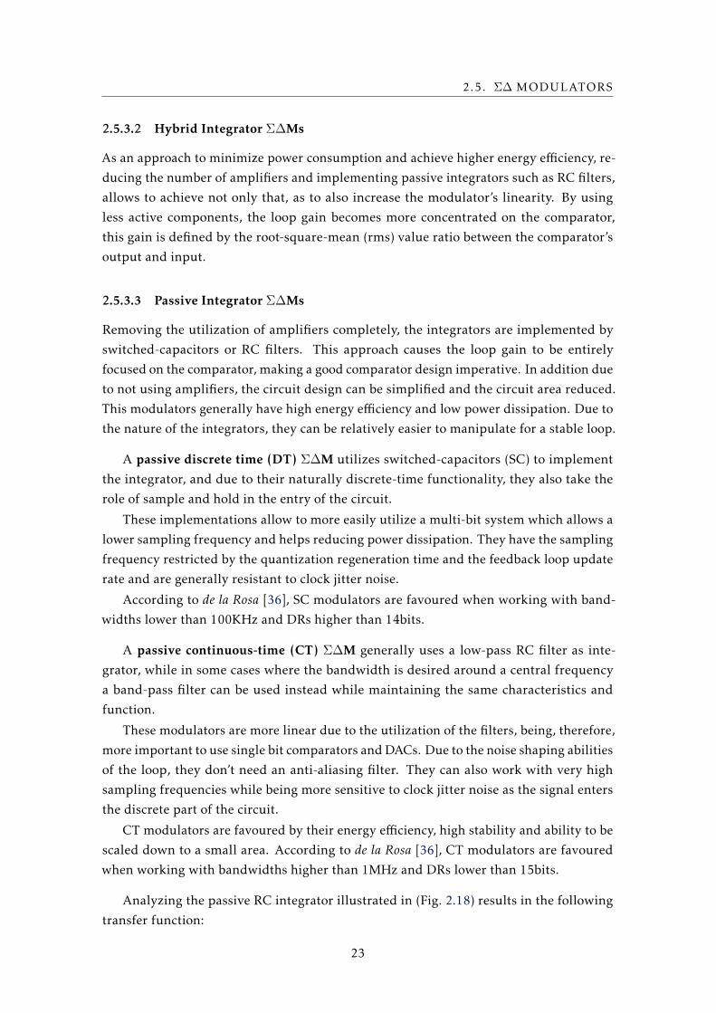
Analyzing the passive RC integrator illustrated in (Fig. 2.18) results in the following
transfer function:
23
CHAPTER 2. STATE OF ART
Figure 2.18: RC passive integratorSource: Reprinted from [37]
H(s) =VoutxVinx
=1
s ∗R1 ∗C1 + 1(2.11)
As seen from expression 2.11, the RC integrator is a low-pass filter with pole frequency
larger than 0Hz, as would be expected, since an ideal integrator is impossible to build.
From further analysis according to [37, 38], due to the attenuated output of the passive
filter, the gain of the comparator will need to be increased accordingly, as to allow the
modulator to have the projected loop gain.
There have been successful attempts at implementations based on this design with
[37–40], such as illustrated in (Fig. 2.19).
(a) (b)Figure 2.19: 2nd order ΣΔM with feedforward structure (a) block diagram (b) circuitrepresentation
Source: Reprinted from [37].
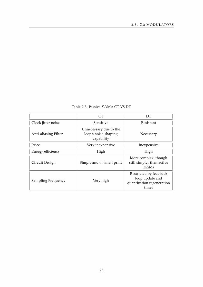
A simplified and illustrative comparison is made in table 2.3 between CT and DT
passive ΣΔMs. In this work, the CT passive ΣΔM was chosen to be implemented, mainly
due to its low cost and simple design.
24
2.5. ΣΔ MODULATORS
Table 2.3: Passive ΣΔMs: CT VS DT
CT DT
Clock jitter noise Sensitive Resistant
Anti-aliasing FilterUnnecessary due to the
loop’s noise-shapingcapability
Necessary
Price Very inexpensive Inexpensive
Energy efficiency High High
Circuit Design Simple and of small printMore complex, thoughstill simpler than active
ΣΔMs
Sampling Frequency Very high
Restricted by feedbackloop update and
quantization regenerationtimes
25

Chapter
3Architecture Development
This chapter presents the solution proposed to complete the objectives defined in 1.2.
Here will be presented the preparatory study for the implementation of the ΣΔmodula-
tor.
3.1 Circuit Design
3.1.1 Theoretical analysis
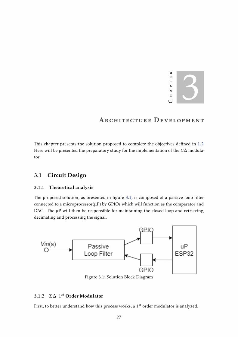
The proposed solution, as presented in figure 3.1, is composed of a passive loop filter
connected to a microprocessor(µP) by GPIOs which will function as the comparator and
DAC. The µP will then be responsible for maintaining the closed loop and retrieving,
decimating and processing the signal.
Figure 3.1: Solution Block Diagram
3.1.2 ΣΔ 1st Order Modulator
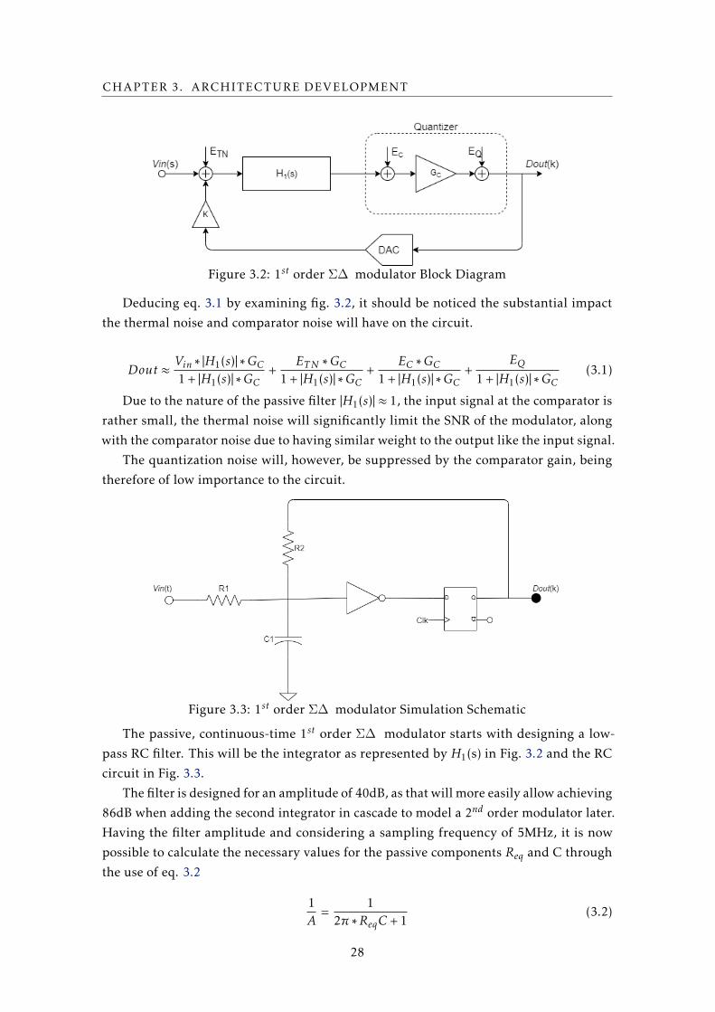
First, to better understand how this process works, a 1st order modulator is analyzed.
27
CHAPTER 3. ARCHITECTURE DEVELOPMENT
Figure 3.2: 1st order ΣΔ modulator Block Diagram
Deducing eq. 3.1 by examining fig. 3.2, it should be noticed the substantial impact
the thermal noise and comparator noise will have on the circuit.
Dout ≈ Vin ∗ |H1(s)| ∗GC1 + |H1(s)| ∗GC
+ETN ∗GC
1 + |H1(s)| ∗GC+
EC ∗GC1 + |H1(s)| ∗GC
+EQ
1 + |H1(s)| ∗GC(3.1)
Due to the nature of the passive filter |H1(s)| ≈ 1, the input signal at the comparator is
rather small, the thermal noise will significantly limit the SNR of the modulator, along
with the comparator noise due to having similar weight to the output like the input signal.
The quantization noise will, however, be suppressed by the comparator gain, being
therefore of low importance to the circuit.
Figure 3.3: 1st order ΣΔ modulator Simulation Schematic
The passive, continuous-time 1st order ΣΔ modulator starts with designing a low-
pass RC filter. This will be the integrator as represented by H1(s) in Fig. 3.2 and the RC
circuit in Fig. 3.3.
The filter is designed for an amplitude of 40dB, as that will more easily allow achieving
86dB when adding the second integrator in cascade to model a 2nd order modulator later.
Having the filter amplitude and considering a sampling frequency of 5MHz, it is now
possible to calculate the necessary values for the passive components Req and C through
the use of eq. 3.2
1A
=1
2π ∗ReqC + 1(3.2)
28
3.1. CIRCUIT DESIGN
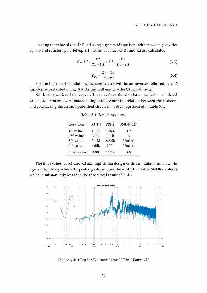
Fixating the value of C at 1nF and using a system of equations with the voltage divider
eq. 3.3 and resistors parallel eq. 3.4 the initial values of R1 and R2 are calculated.
0 = 1.5 ∗ R2R1 +R2
+ 1.5 ∗ R1R1 +R2
(3.3)
Req =R1 +R2R1 ∗R2
(3.4)
For the high-level simulation, the comparator will be an inverter followed by a D
flip-flop as presented in Fig. 3.3. As this will emulate the GPIOs of the µP.
Not having achieved the expected results from the simulation with the calculated
values, adjustments were made, taking into account the relation between the resistors
and considering the already published circuit in [39] as represented in table 3.1.
Table 3.1: Resistors values
Iterations R1[Ω] R2[Ω] SNDR[dB]
1st value 165.5 146.6 192nd value 9.3k 1.1k 33rd value 3.1M 8.86k Undef.4th value 465k 400k Undef.
Final value 930k 3.72M 46
The final values of R1 and R2 accomplish the design of this modulator as shown in
figure 3.4, having achieved a peak signal-to-noise-plus-distortion ratio (SNDR) of 46dB,
which is substantially less than the theoretical result of 71dB.
Figure 3.4: 1st order ΣΔmodulator FFT in LTspice VII
29
CHAPTER 3. ARCHITECTURE DEVELOPMENT
3.2 Simulation programs
The simulations were run on the simulation program LTspiceVII, due to its simplicity
of creating a circuit and running its spice simulation. It should be taken note that all
simulations were extremely slow and processor taxing which shouldn’t, as the circuit is
rather simple. The few reasons for which this might have happened were too much strain
due to the high sampling frequency requested, as well as lack of optimisation on the part
of the inverter and D flip-flop modules.
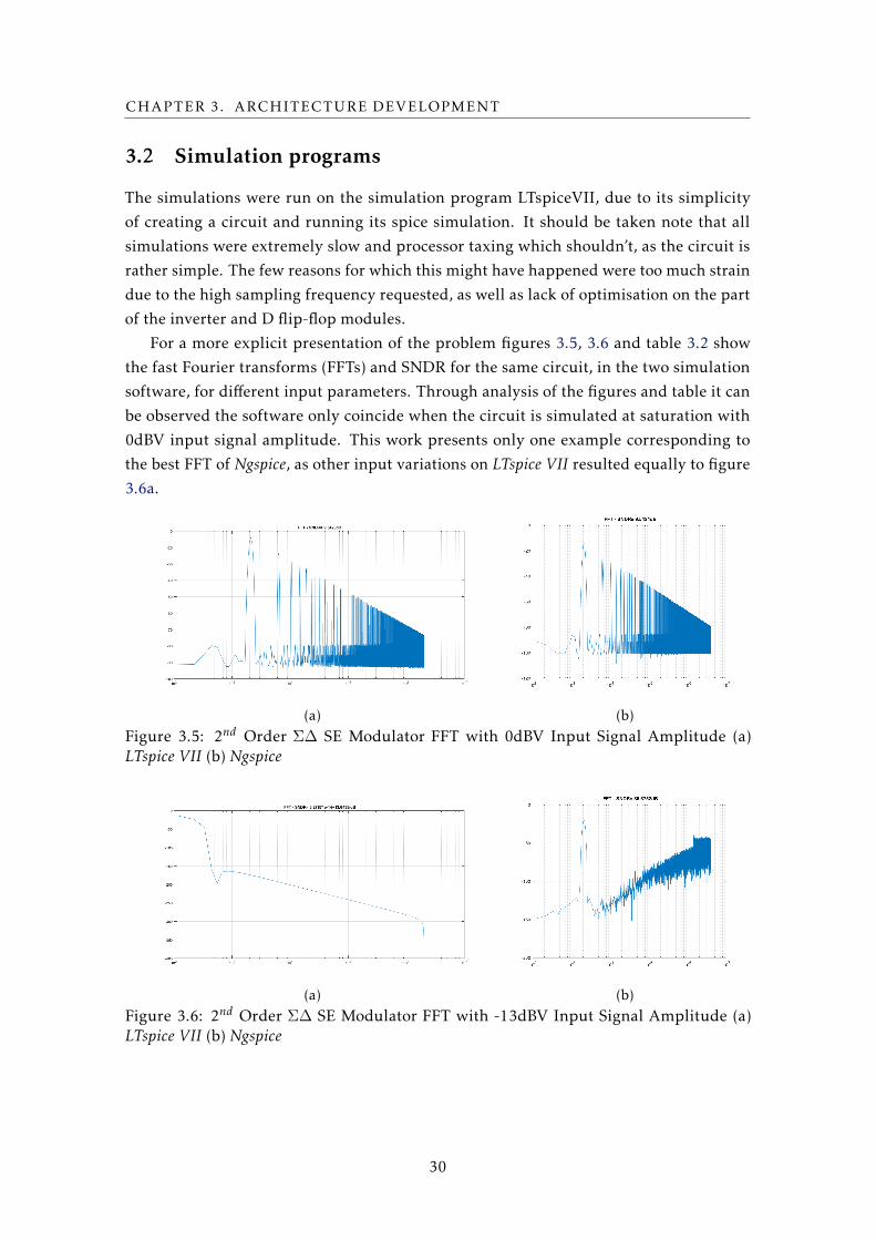
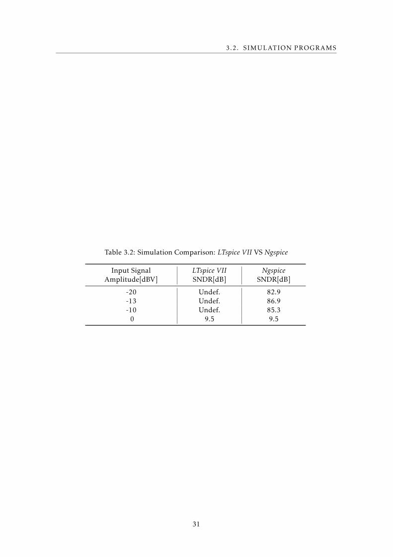
For a more explicit presentation of the problem figures 3.5, 3.6 and table 3.2 show
the fast Fourier transforms (FFTs) and SNDR for the same circuit, in the two simulation
software, for different input parameters. Through analysis of the figures and table it can
be observed the software only coincide when the circuit is simulated at saturation with
0dBV input signal amplitude. This work presents only one example corresponding to
the best FFT of Ngspice, as other input variations on LTspice VII resulted equally to figure
3.6a.
(a) (b)Figure 3.5: 2nd Order ΣΔ SE Modulator FFT with 0dBV Input Signal Amplitude (a)LTspice VII (b) Ngspice
(a) (b)Figure 3.6: 2nd Order ΣΔ SE Modulator FFT with -13dBV Input Signal Amplitude (a)LTspice VII (b) Ngspice
30
3.2. SIMULATION PROGRAMS
Table 3.2: Simulation Comparison: LTspice VII VS Ngspice
Input SignalAmplitude[dBV]
LTspice VIISNDR[dB]
NgspiceSNDR[dB]
-20 Undef. 82.9-13 Undef. 86.9-10 Undef. 85.3
0 9.5 9.5
31

Chapter
4ΣΔ 2nd Order Modulator Development
To achieve an SNDR of 86dB it is necessary to decrease the quantization noise, which
depends on the loop gain.
4.1 ΣΔ 2nd Order Modulator Single Ended
The loop gain inside the signal band for the filter is given by eq. 4.1
|H(fband)| ∗KG =|H(fband)||H(fs/2)|
≈fs
2 ∗ fp(4.1)
where fs is the sampling frequency and fp is the pole frequency. This expression
shows that either by increasing fs or decreasing fp the quantization noise in the signal
band can be suppressed. Due to the goal of the ADC to be a high-resolution voice audio
receiver, the pole frequency is set at 10KHz, which is around the middle of the audible
spectrum, and the sampling frequency is increased to 8MHz.
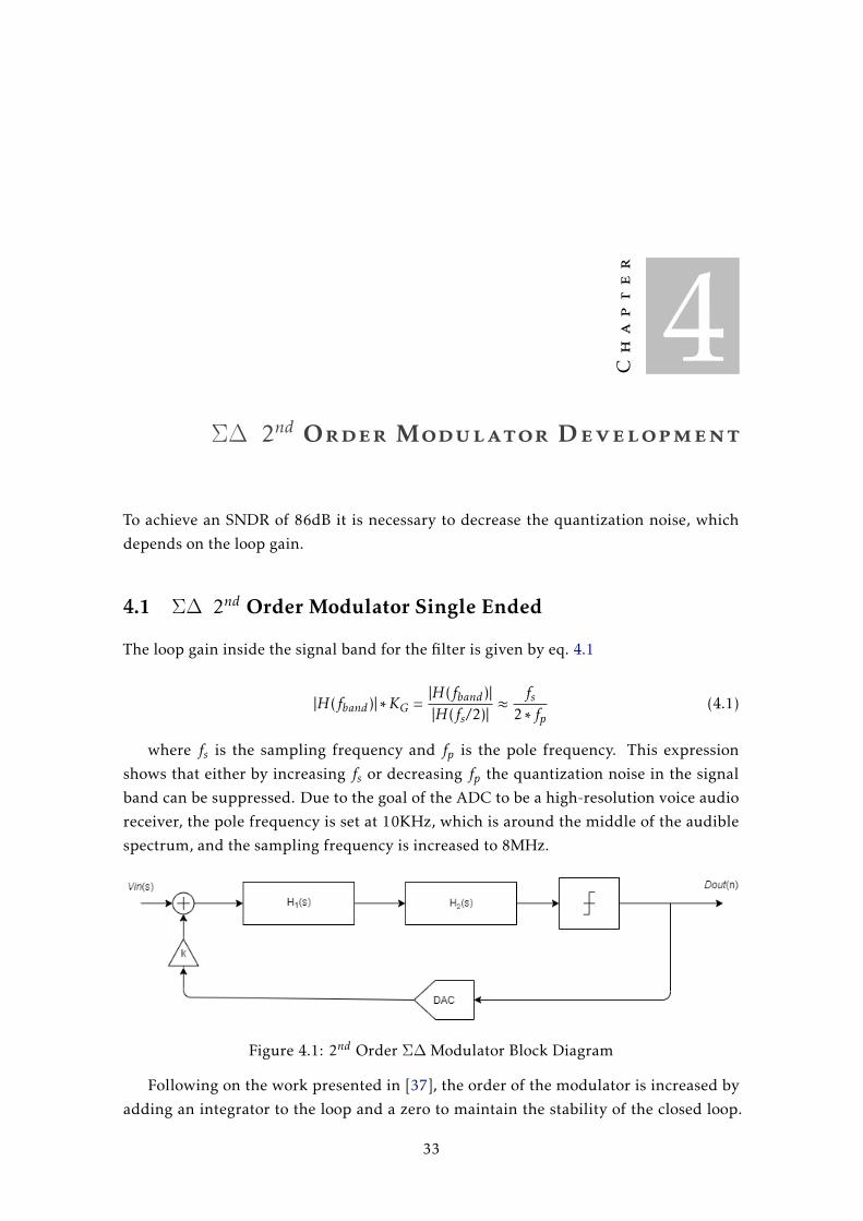
Figure 4.1: 2nd Order ΣΔModulator Block Diagram
Following on the work presented in [37], the order of the modulator is increased by
adding an integrator to the loop and a zero to maintain the stability of the closed loop.
33
CHAPTER 4. ΣΔ 2nd ORDER MODULATOR DEVELOPMENT
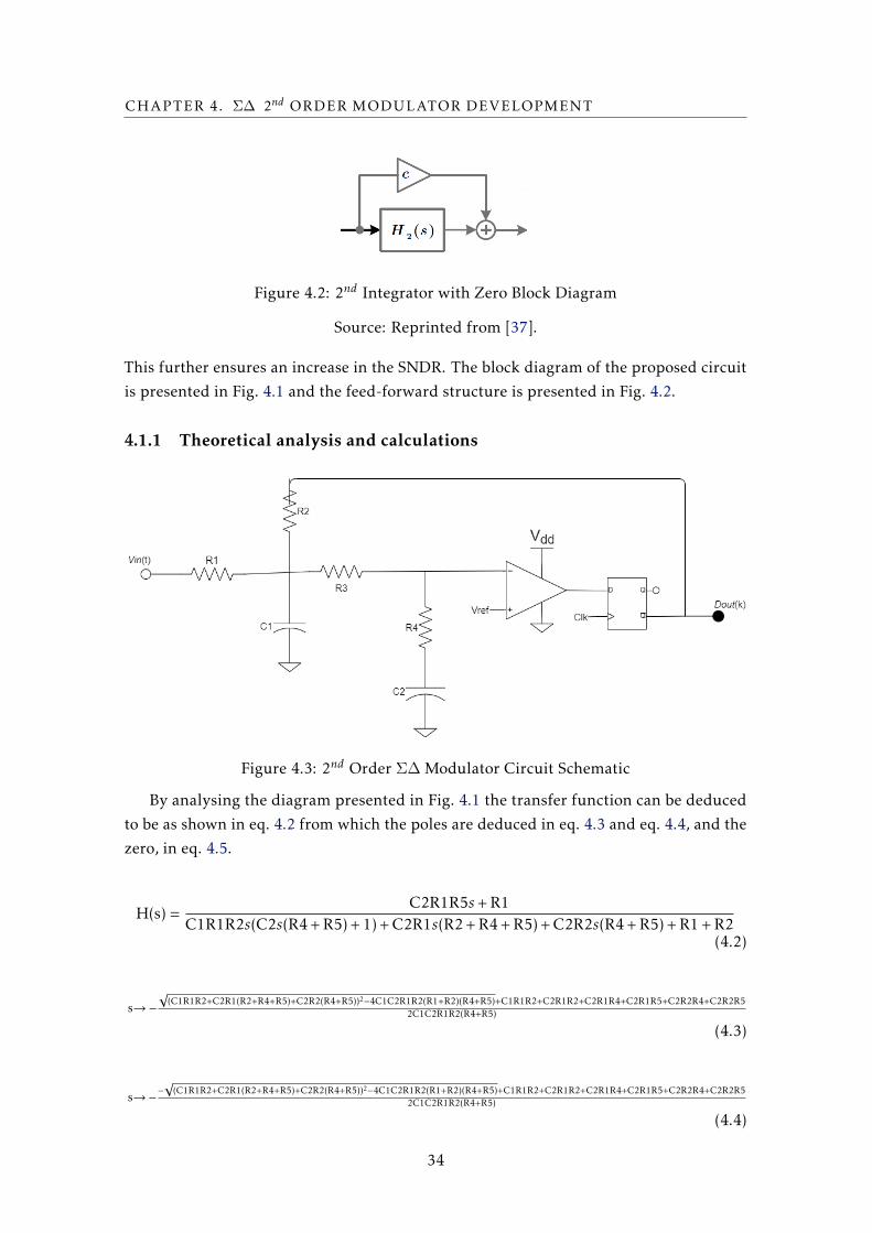
Figure 4.2: 2nd Integrator with Zero Block Diagram
Source: Reprinted from [37].
This further ensures an increase in the SNDR. The block diagram of the proposed circuit
is presented in Fig. 4.1 and the feed-forward structure is presented in Fig. 4.2.
4.1.1 Theoretical analysis and calculations
Figure 4.3: 2nd Order ΣΔModulator Circuit Schematic
By analysing the diagram presented in Fig. 4.1 the transfer function can be deduced
to be as shown in eq. 4.2 from which the poles are deduced in eq. 4.3 and eq. 4.4, and the
zero, in eq. 4.5.
H(s) =C2R1R5s+ R1
C1R1R2s(C2s(R4 + R5) + 1) + C2R1s(R2 + R4 + R5) + C2R2s(R4 + R5) + R1 + R2(4.2)
s→−√
(C1R1R2+C2R1(R2+R4+R5)+C2R2(R4+R5))2−4C1C2R1R2(R1+R2)(R4+R5)+C1R1R2+C2R1R2+C2R1R4+C2R1R5+C2R2R4+C2R2R52C1C2R1R2(R4+R5)
(4.3)
s→−−√
(C1R1R2+C2R1(R2+R4+R5)+C2R2(R4+R5))2−4C1C2R1R2(R1+R2)(R4+R5)+C1R1R2+C2R1R2+C2R1R4+C2R1R5+C2R2R4+C2R2R52C1C2R1R2(R4+R5)
(4.4)
34
4.1. ΣΔ 2nd ORDER MODULATOR SINGLE ENDED
s→− 1C2R5
(4.5)
Due to the complexity of the transfer function represented by equation 4.2, a simpli-
fied version, eq. 4.6, was used for the calculation of the noise transfer function(eq. 4.10).
H(s) =K0Vref ( sz1
+ 1)
( sp1 + 1)( sp2
+ 1)(4.6)
Starting by converting the transfer function(TF) from Laplace domain to time domain
and afterwards to discrete-time, so we can apply the z-transform and arrive at expres-
sion 4.7 which represents the transfer function in z domain.
H(z)=K0Vref ((p1 − p2)z1 + eT clk(p1+p2)z(p1 − p2)z1 + eT clkp1((−1 + z)p1p2 − zp1z1 + p2z1) + eT clkp2(zp2z1 − p1((−1 + z)p2 + z1)))
(−1 + eT clkp2z)2(p1 − p2)z1(4.7)
As the z domain transfer function has been deduced, it is now possible to conclude the
noise transfer function(4.10) by using the comparator gain equation 4.8 and the closed
loop expression 4.9.
KG =1
|H(ej∗2π
4 )|(4.8)
Dout = VNQ −Dout ∗H(z) ∗KG (4.9)
NTF(z)=1
1 +K0Vref ((p1−p2)z1+eT clk(p1+p2)z(p1−p2)z1+eT clkp1 ((−1+z)p1p2−zp1z1+p2z1)+eT clkp1 (zp2z1−p1((−1+z)p2+z1)))
(−1+eT clkp1z)(−1+eT clkp2z)|K0Vref (−i(p1−p2)z1+eT clk(p1+p2)(p1−p2)z1+eT clkp1 ((1+i)p1p2−p1z1−ip2z1)+eT clkp2 ((−1−i)p1p2+ip1z1+p2z1))
(i+eT clkp1 )(i+eT clkp2 )(p1−p2)z1|(p1−p2)z1
(4.10)
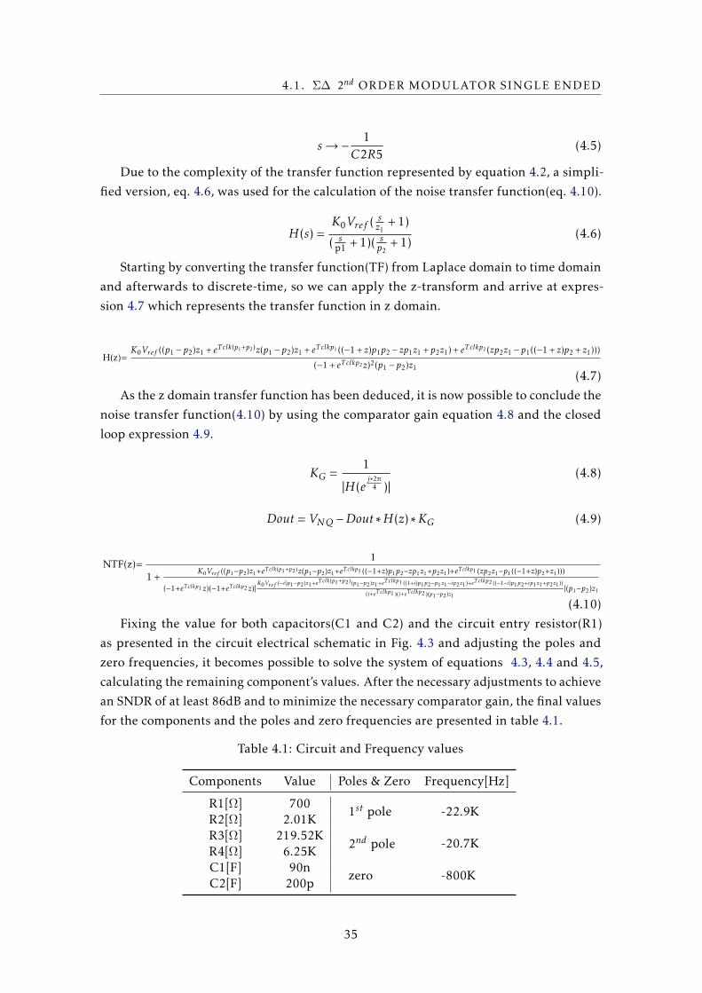
Fixing the value for both capacitors(C1 and C2) and the circuit entry resistor(R1)
as presented in the circuit electrical schematic in Fig. 4.3 and adjusting the poles and
zero frequencies, it becomes possible to solve the system of equations 4.3, 4.4 and 4.5,
calculating the remaining component’s values. After the necessary adjustments to achieve
an SNDR of at least 86dB and to minimize the necessary comparator gain, the final values
for the components and the poles and zero frequencies are presented in table 4.1.
Table 4.1: Circuit and Frequency values
Components Value Poles & Zero Frequency[Hz]
R1[Ω] 7001st pole -22.9K
R2[Ω] 2.01KR3[Ω] 219.52K
2nd pole -20.7KR4[Ω] 6.25KC1[F] 90n
zero -800KC2[F] 200p
35
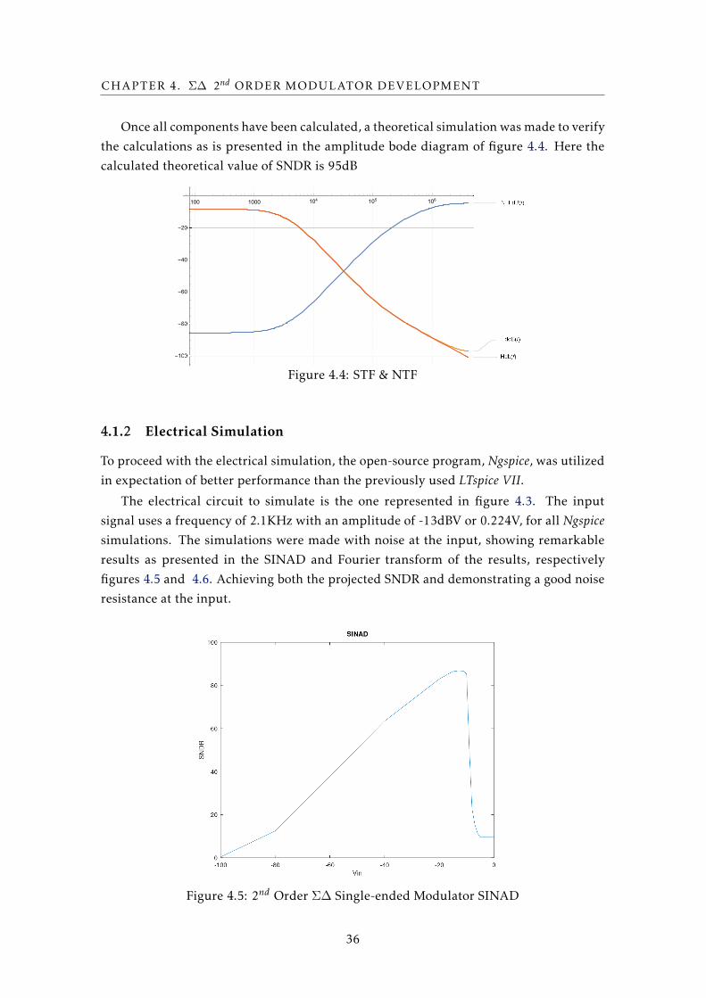
CHAPTER 4. ΣΔ 2nd ORDER MODULATOR DEVELOPMENT
Once all components have been calculated, a theoretical simulation was made to verify
the calculations as is presented in the amplitude bode diagram of figure 4.4. Here the
calculated theoretical value of SNDR is 95dB
100 1000 104
105
106
-100
-80
-60
-40
-20
Figure 4.4: STF & NTF
4.1.2 Electrical Simulation
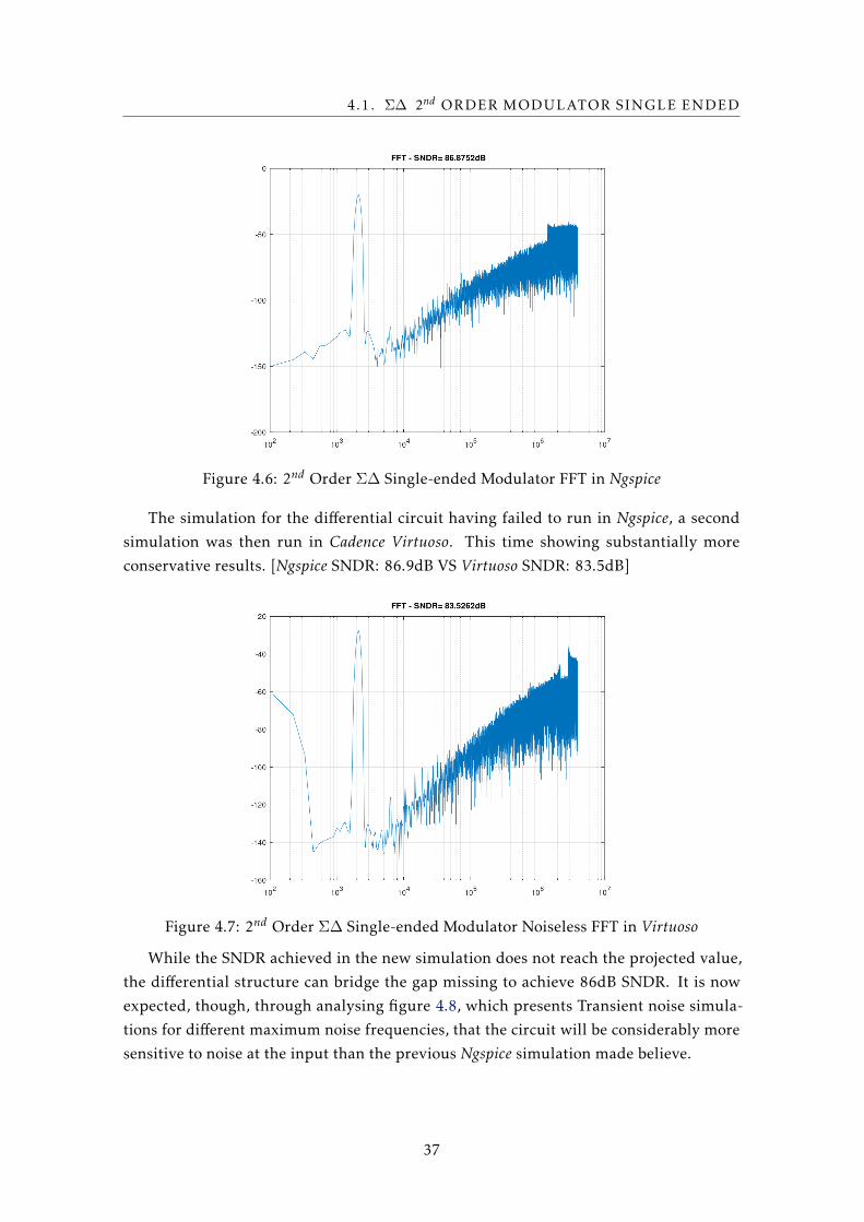
To proceed with the electrical simulation, the open-source program, Ngspice, was utilized
in expectation of better performance than the previously used LTspice VII.
The electrical circuit to simulate is the one represented in figure 4.3. The input
signal uses a frequency of 2.1KHz with an amplitude of -13dBV or 0.224V, for all Ngspicesimulations. The simulations were made with noise at the input, showing remarkable
results as presented in the SINAD and Fourier transform of the results, respectively
figures 4.5 and 4.6. Achieving both the projected SNDR and demonstrating a good noise
resistance at the input.
Figure 4.5: 2nd Order ΣΔ Single-ended Modulator SINAD
36
4.1. ΣΔ 2nd ORDER MODULATOR SINGLE ENDED
Figure 4.6: 2nd Order ΣΔ Single-ended Modulator FFT in Ngspice
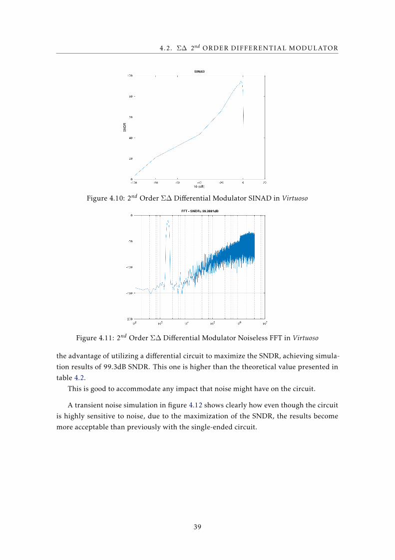
The simulation for the differential circuit having failed to run in Ngspice, a second
simulation was then run in Cadence Virtuoso. This time showing substantially more
conservative results. [Ngspice SNDR: 86.9dB VS Virtuoso SNDR: 83.5dB]
Figure 4.7: 2nd Order ΣΔ Single-ended Modulator Noiseless FFT in Virtuoso
While the SNDR achieved in the new simulation does not reach the projected value,
the differential structure can bridge the gap missing to achieve 86dB SNDR. It is now
expected, though, through analysing figure 4.8, which presents Transient noise simula-
tions for different maximum noise frequencies, that the circuit will be considerably more
sensitive to noise at the input than the previous Ngspice simulation made believe.
37
CHAPTER 4. ΣΔ 2nd ORDER MODULATOR DEVELOPMENT
(a) (b) (c)Figure 4.8: 2nd Order ΣΔ SE Modulator Noise FFT in Virtuoso (a) Noise < 16MHz (b)Noise < 32MHz (c) Noise < 80MHz
4.2 ΣΔ 2nd Order Differential Modulator
A differential structure is used to minimize error and noise interference at the input and
to maximize the SNDR. The fully differential circuit to simulate will be the same as
previously studied, as shown in figure 4.9.
Figure 4.9: 2nd Order ΣΔ Differential Modulator Electrical Schematic
Through the SINAD, it is concluded the best result is obtained for -2.5dBV of input
signal amplitude, as such, all following simulation of the differential circuit will have this
input signal amplitude, while keeping the previous frequency of 2.1KHz.
Table 4.2: Theoretical Results
SNDR[dB] DR[dB]
95 98
The SINAD in figure 4.10 and fast fourier transform(FFT) in figure 4.11 both confirm
38
4.2. ΣΔ 2nd ORDER DIFFERENTIAL MODULATOR
Figure 4.10: 2nd Order ΣΔ Differential Modulator SINAD in Virtuoso
Figure 4.11: 2nd Order ΣΔ Differential Modulator Noiseless FFT in Virtuoso
the advantage of utilizing a differential circuit to maximize the SNDR, achieving simula-
tion results of 99.3dB SNDR. This one is higher than the theoretical value presented in
table 4.2.
This is good to accommodate any impact that noise might have on the circuit.
A transient noise simulation in figure 4.12 shows clearly how even though the circuit
is highly sensitive to noise, due to the maximization of the SNDR, the results become
more acceptable than previously with the single-ended circuit.
39
CHAPTER 4. ΣΔ 2nd ORDER MODULATOR DEVELOPMENT
(a) (b) (c)Figure 4.12: 2nd Order ΣΔ Differential Modulator Noise FFT in Virtuoso (a) Noise <16MHz (b) Noise < 32MHz (c) Noise < 80MHz
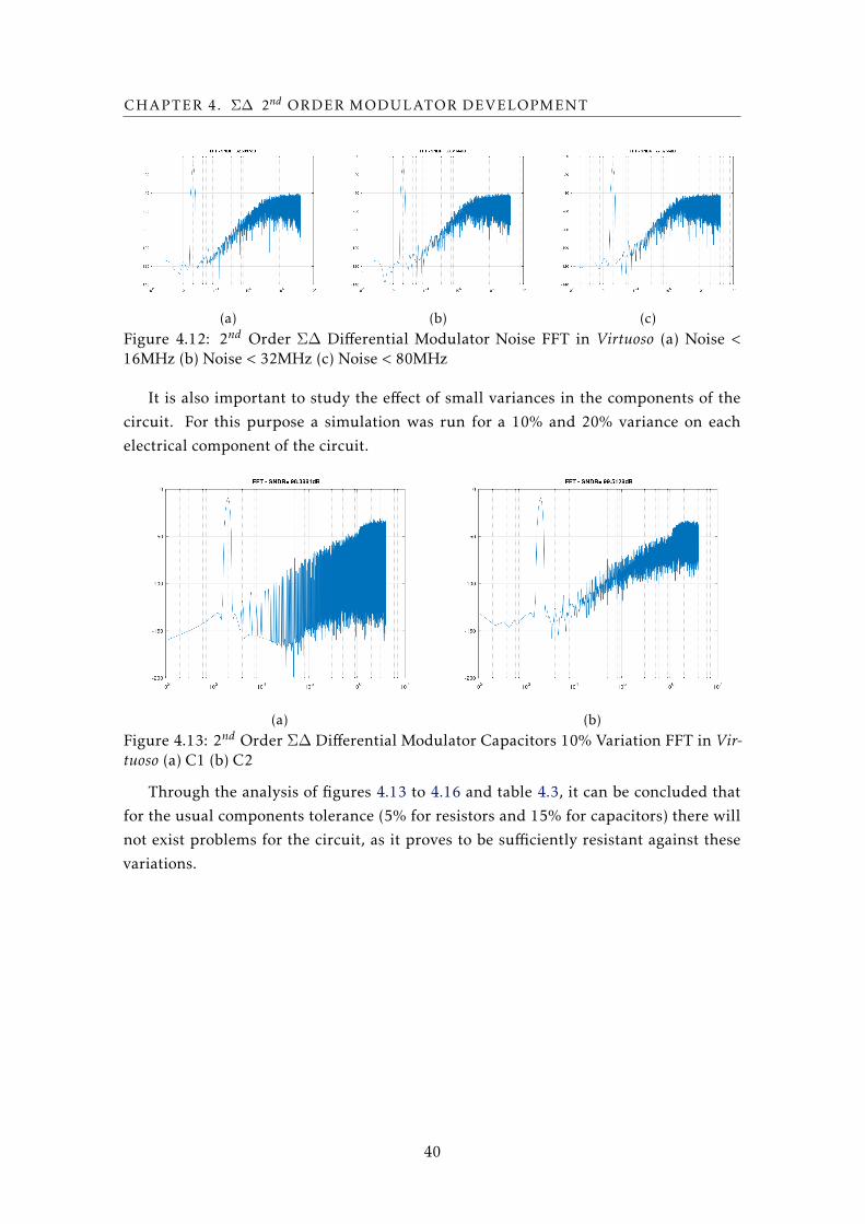
It is also important to study the effect of small variances in the components of the
circuit. For this purpose a simulation was run for a 10% and 20% variance on each
electrical component of the circuit.
(a) (b)Figure 4.13: 2nd Order ΣΔ Differential Modulator Capacitors 10% Variation FFT in Vir-tuoso (a) C1 (b) C2
Through the analysis of figures 4.13 to 4.16 and table 4.3, it can be concluded that
for the usual components tolerance (5% for resistors and 15% for capacitors) there will
not exist problems for the circuit, as it proves to be sufficiently resistant against these
variations.
40
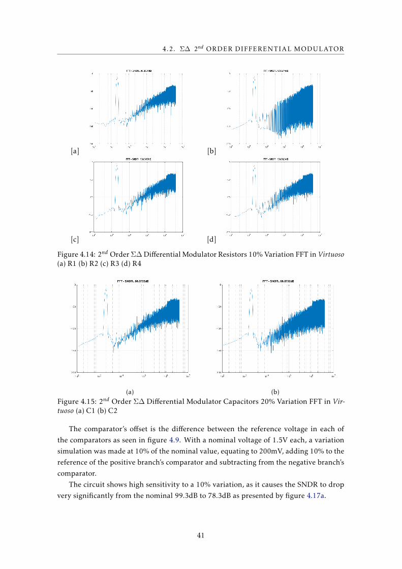
4.2. ΣΔ 2nd ORDER DIFFERENTIAL MODULATOR
[a] [b]
[c] [d]
Figure 4.14: 2nd OrderΣΔDifferential Modulator Resistors 10% Variation FFT in Virtuoso(a) R1 (b) R2 (c) R3 (d) R4
(a) (b)Figure 4.15: 2nd Order ΣΔ Differential Modulator Capacitors 20% Variation FFT in Vir-tuoso (a) C1 (b) C2
The comparator’s offset is the difference between the reference voltage in each of
the comparators as seen in figure 4.9. With a nominal voltage of 1.5V each, a variation
simulation was made at 10% of the nominal value, equating to 200mV, adding 10% to the
reference of the positive branch’s comparator and subtracting from the negative branch’s
comparator.
The circuit shows high sensitivity to a 10% variation, as it causes the SNDR to drop
very significantly from the nominal 99.3dB to 78.3dB as presented by figure 4.17a.
41
CHAPTER 4. ΣΔ 2nd ORDER MODULATOR DEVELOPMENT
[a] [b]
[c] [d]
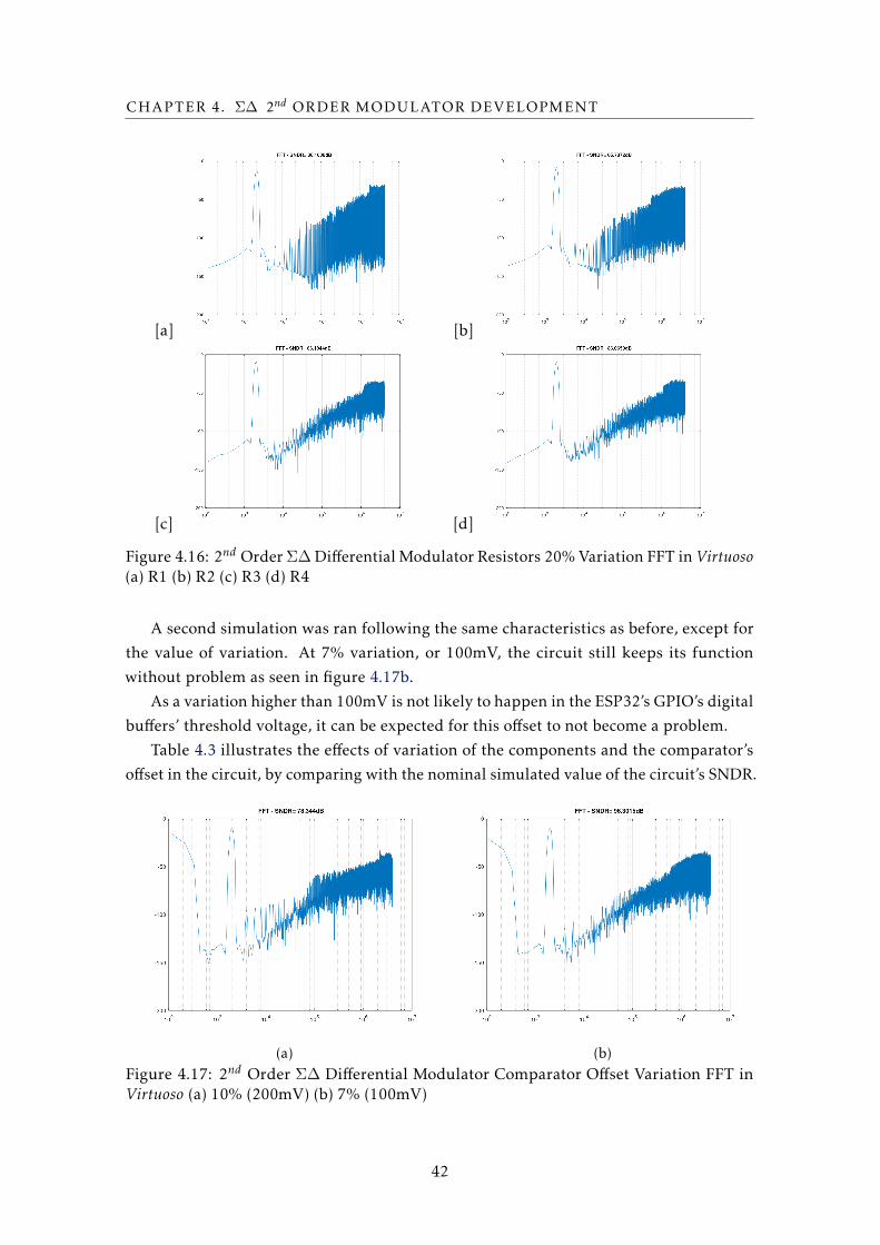
Figure 4.16: 2nd OrderΣΔDifferential Modulator Resistors 20% Variation FFT in Virtuoso(a) R1 (b) R2 (c) R3 (d) R4
A second simulation was ran following the same characteristics as before, except for
the value of variation. At 7% variation, or 100mV, the circuit still keeps its function
without problem as seen in figure 4.17b.
As a variation higher than 100mV is not likely to happen in the ESP32’s GPIO’s digital
buffers’ threshold voltage, it can be expected for this offset to not become a problem.
Table 4.3 illustrates the effects of variation of the components and the comparator’s
offset in the circuit, by comparing with the nominal simulated value of the circuit’s SNDR.
(a) (b)Figure 4.17: 2nd Order ΣΔ Differential Modulator Comparator Offset Variation FFT inVirtuoso (a) 10% (200mV) (b) 7% (100mV)
42
4.2. ΣΔ 2nd ORDER DIFFERENTIAL MODULATOR
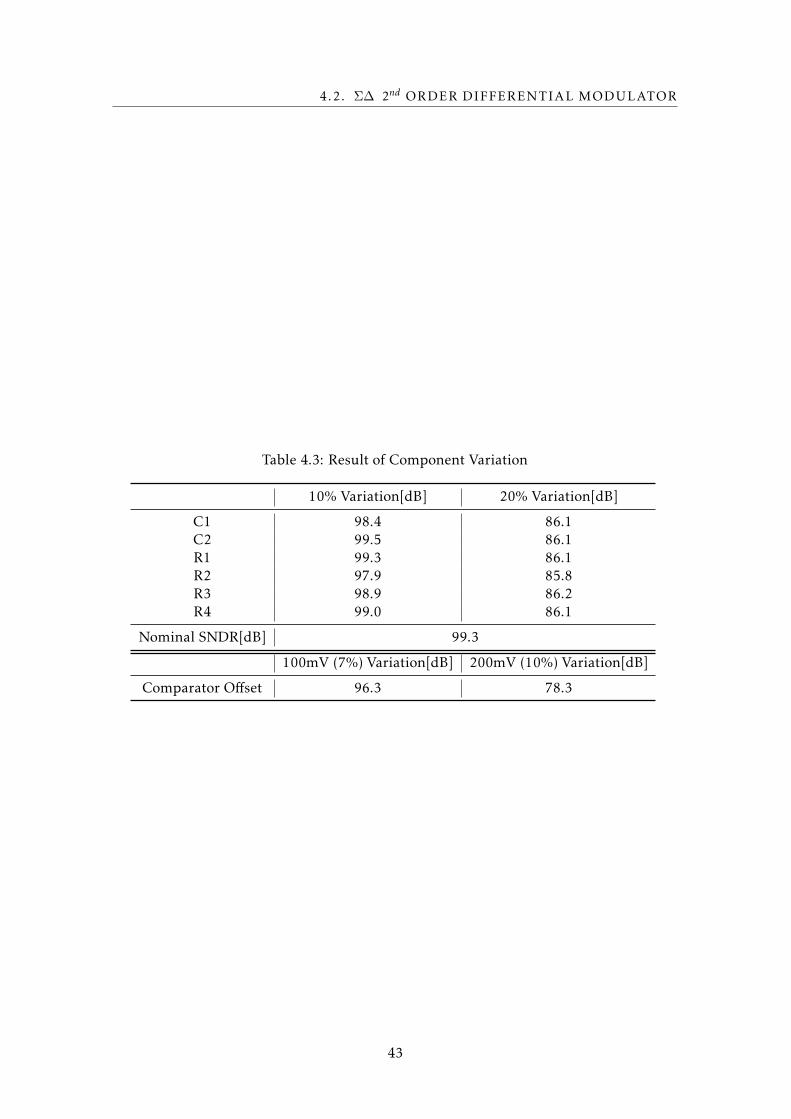
Table 4.3: Result of Component Variation
10% Variation[dB] 20% Variation[dB]
C1 98.4 86.1C2 99.5 86.1R1 99.3 86.1R2 97.9 85.8R3 98.9 86.2R4 99.0 86.1
Nominal SNDR[dB] 99.3
100mV (7%) Variation[dB] 200mV (10%) Variation[dB]
Comparator Offset 96.3 78.3
43

Chapter
5ESP32 Development & Implementation
After the circuit is studied and simulated, this chapter presents the study for the imple-
mentation of the circuit with the chosen µP.
5.1 Viability Study for ESP32
5.1.1 Theoretical Viability Study
To know whether the ESP32 will be able to take on the work of digital decimation filter
and DAC, there needs to be a study on the speed of CPU operations.
According to community benchmarks [41], at 240MHz clock frequency, or one clock
every 4,17ns, the ESP32 can do one integer addition operation in 1.6ns, and one integer
multiplication operation in 23.4ns. This corresponds to one clock cycle per addition
operation and six clock cycles per multiplication operation.
It needs to be considered that this test was at full power without interference. For a
better understanding of how the processing of the digital output from theΣΔM should be
done, and considering the ultra low power capabilities (ULP) of the ESP32 more testing
should be done with the ULP co-processor, which has a frequency of 8MHz to 40MHz.
In order to achieve the best optimization of quality, cost and power-efficiency, it is
important to know the range of specifications of the ΣΔM ADC
According to the table 2.2 in page 9, to which can be added the limitation range of
DR and values per sample, [74dB - 98dB] and [4096 - 65536] respectively, a compromise
can then be made after the prioritization of specifications to consider.
A fundamental task the esp32 must accomplish is the feedback of the circuit, this
would require to synchronize both the GPIOs connected to the filters, as shown previously
in figure 3.1. The way to do this is through the use of either external or software interrupts,
45
CHAPTER 5. ESP32 DEVELOPMENT & IMPLEMENTATION
however, as the interrupts take 2.5µs to solve it is too slow to maintain the projected 8MHz
sampling frequency.
5.1.2 Practical Viability Study
An issue came up with the initially chosen programming environment, Arduino IDE.
The GPIOs could not transmit a signal with a frequency higher than 1MHz, due to the
way the environment itself programs the low-level code, to guarantee compatibility be-
tween C++, its programming language, and C, the language in which the esp-IDF is
programmed. To solve this, another programming environment was used, an extension
of Visual Studio Code, PIO. This allowed the integration of both Arduino and esp-IDF
libraries, independently from which programming language was chosen.
Regardless of the inability to utilize interrupts to keep synchronous action between
the GPIOs, due to the high sampling frequency, there is a possibility the µP can keep
the signal flowing well on its own. Therefore, a simple test was made, which consisted
of generating an external square signal to enter through one GPIO and exit through one
different one, where it would be read by an oscilloscope. From the oscilloscope results
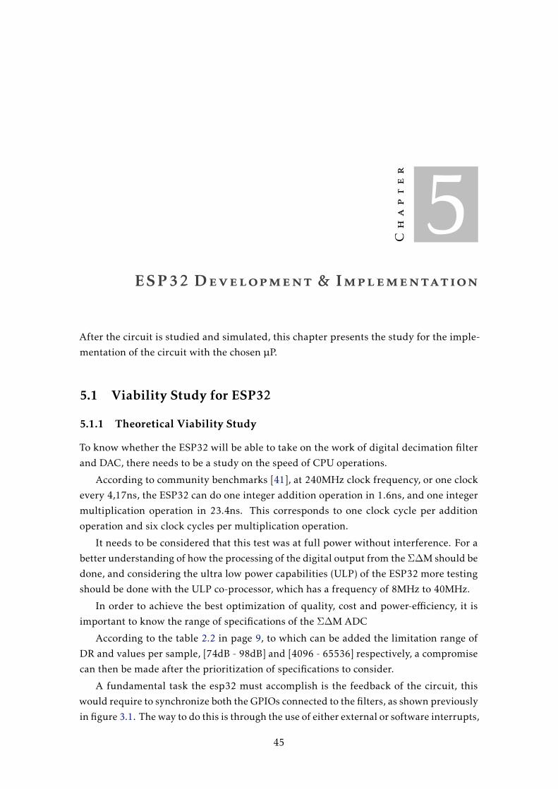
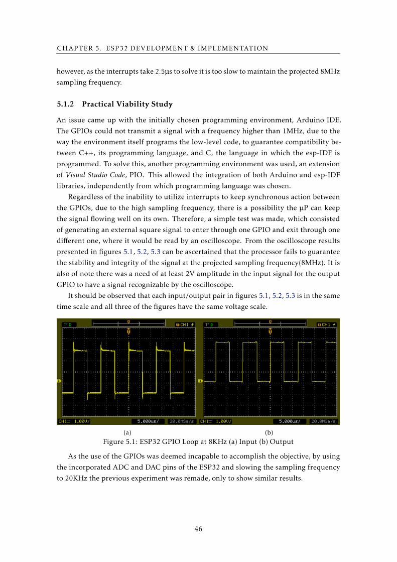
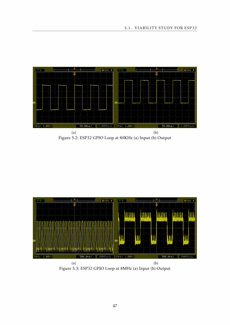
presented in figures 5.1, 5.2, 5.3 can be ascertained that the processor fails to guarantee
the stability and integrity of the signal at the projected sampling frequency(8MHz). It is
also of note there was a need of at least 2V amplitude in the input signal for the output
GPIO to have a signal recognizable by the oscilloscope.
It should be observed that each input/output pair in figures 5.1, 5.2, 5.3 is in the same
time scale and all three of the figures have the same voltage scale.
(a) (b)Figure 5.1: ESP32 GPIO Loop at 8KHz (a) Input (b) Output
As the use of the GPIOs was deemed incapable to accomplish the objective, by using
the incorporated ADC and DAC pins of the ESP32 and slowing the sampling frequency
to 20KHz the previous experiment was remade, only to show similar results.
46
5.1. VIABILITY STUDY FOR ESP32
(a) (b)Figure 5.2: ESP32 GPIO Loop at 80KHz (a) Input (b) Output
(a) (b)Figure 5.3: ESP32 GPIO Loop at 8MHz (a) Input (b) Output
47

Chapter
6Summary & Future Work
6.1 Summary
In this work, a 2nd order CT ΣΔ modulator employing passive RC integrators with at
least 86dB SNDR was proposed. A differential pair structure maximized the loop gain and
minimized input noise, to try and minimize the necessary comparator gain. The circuit
was optimized to keep the loop gain as independent from the comparator’s as possible.
Nevertheless, due to the high attenuation of the signal by the passive integrators the
comparator’s noise substantially limits the gain.
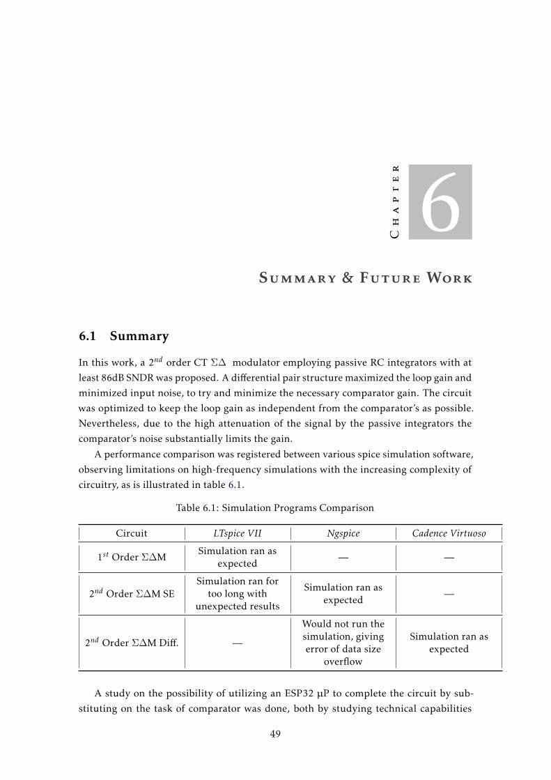
A performance comparison was registered between various spice simulation software,
observing limitations on high-frequency simulations with the increasing complexity of
circuitry, as is illustrated in table 6.1.
Table 6.1: Simulation Programs Comparison
Circuit LTspice VII Ngspice Cadence Virtuoso
1st Order ΣΔMSimulation ran as
expected— —
2nd Order ΣΔM SESimulation ran for
too long withunexpected results
Simulation ran asexpected
—
2nd Order ΣΔM Diff. —
Would not run thesimulation, givingerror of data size
overflow
Simulation ran asexpected
A study on the possibility of utilizing an ESP32 µP to complete the circuit by sub-
stituting on the task of comparator was done, both by studying technical capabilities
49
CHAPTER 6. SUMMARY & FUTURE WORK
and by testing them. Due to hardware limitations of the ESP32, it was not able to work
according to the required high-frequency, thus being deemed inappropriate to substitute
the comparator block in a CT passive ΣΔM.
6.2 Future Work
Despite the circuit not being viable to work in the desired fashion with the ESP32, it might
be possible to substitute the comparator with a µP that can overcome these hardware
limitations in the GPIOs.
It can be interesting to study optimization of the circuit with different approaches
in which the sampling frequency can be reduced, making the circuit more compatible
with the use of µP in exchange of a comparator. It is also important to verify approaches
which cause less attenuation to the input signal of the comparator block and therefore
make more resistant to the comparator’s noise.
Other implementations of passive ΣΔM might also cover some of the limitations no-
ticed along with this work, such as the use of SC filters and using multi-bit techniques,
which would allow to use a significantly lower sampling frequency and keep the resolu-
tion of the modulator intact.
50
Bibliography
[1] M. Conner. “Sensors empower the ’Internet of Things’.” In: EDN (2010), pp. 31–37.
[2] M. A. A. Ahasan. “Smart Home Automation Based on Voice Command Using Smart
Phone.” In: International Journal of Advances in Computer and Electronics Engineering2.2 (2017), pp. 34 –40.
[3] N. Prathima, P Sai Kumar, S. L. Ahmed, and G. Chakradhar. “Voice Recognition
Based Home Automation System for Paralyzed People.” In: International Journalfor Modern Trends in Science and Technology 03.02 (2017), pp. 101–106. url: http:
//ijmtst.com/ncee2017/23.NCEE\_24.pdf.
[4] D. Purohit and M. Ghosh. “Challenges and Types of Home Automation Systems.”
In: International Journal of Computer Science and Mobile Computing 6.4 (2017), pp. 369–
375.
[5] Amazon. Vocca Pro Light - Smart Lights - Voice Activated Lights Adapter - Record YourOwn Voice Triggers - - Amazon.com. url: https://www.amazon.com/Vocca-Pro-
Light-Activated-Triggers/dp/B018QS3P68 (visited on 02/11/2019).
[6] Verbal Machines. VPRO Vocca Pro Voice Activated Bulb Adapter User Manual VoccaPro - Users Manual Activocal LTD. url: https://fccid.io/2ADI5-VPRO/User-
Manual/User-Manual-2547185 (visited on 02/11/2019).
[7] Honeywell. Honeywell Wifi Smart Thermostat with Voice Control - RTH9590WF |Honeywell Store. url: https://www.honeywellstore.com/store/products/wi-
fi-smart-thermostat-with-voice-rth9590wf1003u.htm (visited on 02/05/2019).
[8] Amazon. Honeywell Wi-Fi 7-Day Programmable Thermostat (RTH6580WF), RequiresC Wire, Works with Alexa - - Amazon.com. url: https : / / www . amazon . com /
Honeywell-Programmable-Thermostat-RTH6580WF-Requires/dp/B00Y6M2OUC/
ref=sr\_1\_3?ie=UTF8\&qid=1549912687\&sr=8-3\&keywords=
honeywell+thermostat (visited on 02/11/2019).
[9] Amazon. Echo Dot (3rd Generation) | Alexa-enabled Bluetooth Speaker. url: https:
/ / www . amazon . com / All - new - Echo - Dot - 3rd - Gen / dp / B0792KTHKJ / ref =
sr\_1\_cc\_1?s=aps\&ie=UTF8\&qid=1549374695\&sr=1-1-
catcorr\&keywords=echo+dot+3rd+generation (visited on 02/05/2019).
51
BIBLIOGRAPHY
[10] Apple. HomePod - Apple. url: https://www.apple.com/homepod/ (visited on
02/05/2019).
[11] K. J. Ryan. 7 of the World’s Most Accurate Voice Recognition Systems | Inc.com. 2016.
url: https : / / www . inc . com / kevin - j - ryan / internet - trends - 7 - most -
accurate-word-recognition-platforms.html (visited on 02/05/2019).
[12] Mycroft. About Mycroft - Mycroft. url: https://mycroft.ai/documentation/
mycroft-software-hardware/ (visited on 02/05/2019).
[13] P. Schoutsen. Perfect Home Automation - Home Assistant. url: https : / / www .
home-assistant.io/blog/2016/01/19/perfect-home-automation/ (visited on
02/06/2019).
[14] B. Raj and R. Singh. Design and Implementation of Speech Recognition Systems Class2: Data Capture. 2013.
[15] S. W. Smith. “Chapter 22: Audio Processing.” In: The Scientist and Engineer’s Guideto Digital Signal Processing. 1. 2013, pp. 2–5.
[16] N. Kolban. Kolban’s Book on ESP32. September. Unpublished entry, 2018, p. 1228.
[17] ESP32-DevKitC Development Boards - Espressif Systems | Mouser Portugal. url:
https://pt.mouser.com/new/espressif/espressif-esp32-devkitc-boards/
(visited on 02/14/2019).
[18] Arduino Introduction. url: https://www.arduino.cc/en/Guide/Introduction
(visited on 02/14/2019).
[19] Arduino Micro. url: https://store.arduino.cc/arduino-micro (visited on
02/14/2019).
[20] Raspberry Pi Foundation. What is a Raspberry Pi? url: https://www.raspberrypi.
org/help/what-is-a-raspberry-pi/ (visited on 02/06/2019).
[21] Raspberry Pi Zero v1.3 - KUBII. url: https://www.kubii.fr/pi-zero-v13/1401-
raspberry-pi-zero-v13-kubii-3272496006973.html (visited on 02/06/2019).
[22] Raspberry Pi 2 Model B - Raspberry Pi. url: https://www.raspberrypi.org/
products/raspberry-pi-2-model-b/ (visited on 02/14/2019).
[23] A. Allan. The RDA5981, an ESP8266 Competitor? – Hackster Blog. url: https:
//blog.hackster.io/the-rda5981-an-esp8266-competitor-da161c9c37e2
(visited on 02/07/2019).
[24] T. R. Manual. “Technical Reference Manual.” In: (2018).
[25] Atmel. “ATmega16U4/ATmega32U4 Datasheet.” In: (2016). url: http://ww1.
microchip.com/downloads/en/DeviceDoc/Atmel-7766-8-bit-AVR-ATmega16U4-
32U4\_Datasheet.pdf.
[26] ElectroDragon RDA5981a-WIFI. url: https : / / www . electrodragon . com / w /
RDA5981 (visited on 02/14/2019).
52
BIBLIOGRAPHY
[27] B. Razavi. Principles of Data Conversion System Design. IEEE Press, 1995, p. 134.
[28] J. M. de la Rosa. SIGMA-DELTA CONVERTERS Practical Design Guide. 2nd. Wiley-
IEEE Press, 2018, p. 533. isbn: 9781119275756.
[29] A. V. Oppenheim and R. W. Schafer. Discrete-Time Signal Processing. 3rd. Pearson
Higher Education, Inc., 2009, p. 1108. isbn: 0131988425.
[30] J. M. De La Rosa. “Sigma-delta modulators: Tutorial overview, design guide, and
state-of-the-art survey.” In: IEEE Transactions on Circuits and Systems I: RegularPapers 58.1 (2011), pp. 1–21. issn: 15498328. doi: 10.1109/TCSI.2010.2097652.
[31] NAtionnal Instruments Corp. Benefits of Delta-Sigma Analog-to-Digital Conversion -National Instruments. 2017. url: http://www.ni.com/white-paper/11342/en/
(visited on 02/13/2019).
[32] B. Nowacki. “Design of Sigma-Delta Modulators for Analog-to-Digital Conversion
Intensively Using Passive Circuits.” In: (2016), p. 151. url: http://hdl.handle.
net/10362/18507.
[33] S. Pavan, R. Schreier, and G. C. Temes. “Sampling , Oversampling , and Noise-
shaping.” In: Understanding Delta-Sigma Data Converters. 10.1002/97. 2017, pp. 27–
61. doi: 10.1002/9781119258308.ch2.
[34] B. Baker. Best of Baker’s Best Precision Data Converters Delta-Sigma ADCs. Texas
Instruments Incorporated, 2015, p. 19.
[35] K. Matsukawa, Y. Mitani, M. Takayama, K. Obata, S. Dosho, and A. Matsuzawa.
“A Fifth-Order Continuous-Time Delta-Sigma Modulator With Single-Opamp Res-
onator.” In: IEEE Journal of Solid-State Circuits 45.4 (2010), pp. 697–706.
[36] J. M. De La Rosa. “An empirical and statistical comparison of state-of-the-art
sigma-delta modulators.” In: Proceedings - IEEE International Symposium on Circuitsand Systems (2013), pp. 825–828. issn: 02714310. doi: 10.1109/ISCAS.2013.
6571974.
[37] J. L. De Melo, N. Paulino, and J. Goes. “Continuous-time delta-sigma modulators
based on passive RC integrators.” In: IEEE Transactions on Circuits and Systems I:Regular Papers 65.11 (2018), pp. 3662–3674. issn: 15498328. doi: 10.1109/TCSI.
2018.2855649.
[38] J. L. A. D. Melo. “Sigma-Delta Modulators with Passive RC Integrators : Theory
, Design Methodology for Optimization and Silicon Results Motivation Σ∆ Ms –
Background / Trends Passive versus Active ∆Σ Ms Proposed Idea Proposed Circuit
/ Implementation Measurement Results Co.” Doctoral dissertation. FCT - Univer-
sidade Nova de Lisboa, 2017.
53
BIBLIOGRAPHY
[39] J. L. De Melo. “A low power 1-MHz continuous-time Σ∆M Using a passive loop
filter designed with a genetic algorithm tool.” In: Proceedings - IEEE InternationalSymposium on Circuits and Systems 1 (2013), pp. 586–589. issn: 02714310. doi:
10.1109/ISCAS.2013.6571910.
[40] J. L. De Melo, P. V. Leitao, J. Goes, and N. Paulino. “A simple clab-D audio power
amplifier using a pabive CT Σ∆ modulator for medium quality sound systems.” In:
Proceedings of the 22nd International Conference Mixed Design of Integrated Circuitsand Systems, MIXDES 2015 (2015), pp. 543–546. issn: 0044-4251 (Print). doi:
10.1109/MIXDES.2015.7208582.
[41] url: https://www.esp32.com/viewtopic.php?f=14&t=800&start=20 (visited
on 02/15/2019).
54